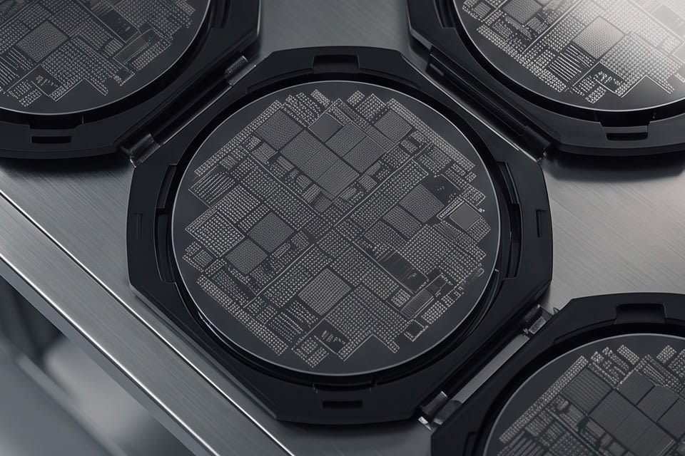
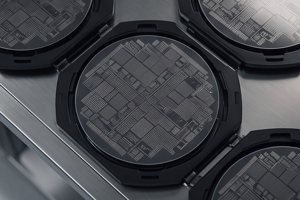
According to an analysis by Yole Group, a semiconductor packaging market research firm, the advanced packaging market is expected to grow by more than 10% annually through 2027, with the share of products adopting chip stacking structures expanding rapidly. As stacking chips in multiple layers becomes a core method for achieving higher performance, thickness uniformity and surface flatness between each layer are emerging as the most sensitive variables determining product reliability. What this figure shows is not simply market growth. It reflects the reality that as stacking structures become more complex, the process costs and yield losses caused by failed flatness control increase as well.
Why flatness is critical in the chip stacking process
In the process of stacking chips layer by layer, flatness is not merely an external appearance standard. Flatness, as defined by SEMI M1, an international semiconductor standards organization, numerically represents how much a wafer surface deviates from an ideal reference plane. In processes below 10 nanometers, total thickness variation (TTV, Total Thickness Variation) must be maintained below 1 micrometer, and the moment this standard is exceeded, the entire subsequent bonding process becomes unstable.
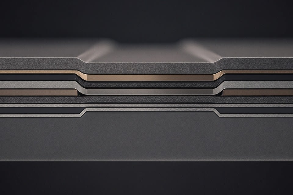
The issue lies in the stacking structure itself. Thickness variation in the temporary bonding layer between chips determines the lower limit of grinding uniformity, and the nonuniformity that occurs in that layer is directly transferred to the next process step. A deviation created in just one layer can expand into alignment error across the entire stacked structure. This becomes even more pronounced in products such as AI semiconductors and high performance memory, where dozens of chips must be stacked. As the number of stacked layers increases, the speed at which initial flatness deviations accumulate also accelerates.
In production sites, flatness defects usually become an issue after the grinding process, when subsequent processes are already underway. This creates a structure in which losses increase the later defects are detected.

Technical design of the PKG Grinder and its response to flatness requirements
The PKG Grinder addresses this issue at the equipment design level. To secure flatness in the grinding process, two conditions must be satisfied at the same time.
- The precision of the stage that holds the package firmly so it does not move during processing
- The cutting precision of the diamond wheel that uniformly removes the surface
The PKG Grinder combines a high precision stage with a diamond wheel to achieve micron-level thickness control. Whether the package type is FCBGA, WLCSP, QFN·DFN, or solar cell, the core role of this equipment is to process it uniformly to the target thickness required by the customer. No matter what package is handled, the standard is the same. It must be ground without deviation until the target thickness is reached.
Depending on the production line configuration, users can choose from Full Auto (Type A·Type B) and Manual Type, enabling line design that considers both the level of automation and process flexibility. The design direction of this equipment is to improve yield by stably maintaining processing quality even under high speed process conditions. Ultimately, flatness control depends on how consistently and precisely grinding equipment handles the surface with controlled force and accurate motion paths.

Quality control extending to post grinding processes
Flatness control is not complete simply because grinding has ended. After grinding, the surface condition must be inspected precisely, and the detection limit of modern inspection systems using laser scattering is approximately 20 to 30 nanometers. However, actual sensitivity varies greatly depending on the wafer surface condition. If residual contamination or fine scratches remain on the surface after grinding, the inspection accuracy itself may decline.
There are also requirements that the contact surface roughness of packaging substrates must be controlled below 20 nanometers, and further below 5 nanometers, to form fine wiring. To reliably secure this level of surface quality, the precision of the cleaning process after grinding is also important. If the connection between grinding and cleaning is broken, it becomes difficult to guarantee precision at the inspection stage.
As demand for AI semiconductors and high performance memory increases, the number of stacked layers and package complexity continue to rise. In a trend where required flatness standards and surface quality standards are becoming stricter at the same time, an integrated approach that covers the entire process is becoming increasingly important, beyond the performance of grinding equipment alone.

The growth figure for the advanced packaging market mentioned in the first sentence ultimately leads to one question. In a situation where more chips must be stacked more thinly, how can flatness be maintained consistently. Only when the entire process, starting with the precision of grinding equipment and continuing through cleaning and inspection, is aligned to a single standard can the reliability of stacked structures be secured. In the chip stacking process, flatness control is not an issue of a single piece of equipment, but an issue of overall process design.
Huvics is an advanced technology company that develops and manufactures automation equipment and
production systems across the semiconductor, LED, Mobile, and Cosmetic industries.
With outstanding talent and continuous technological innovation, we support customers in improving productivity and
securing quality competitiveness.
Huvics Contact
Phone: 031-374-8285
Email: cdpark@huvics.com
