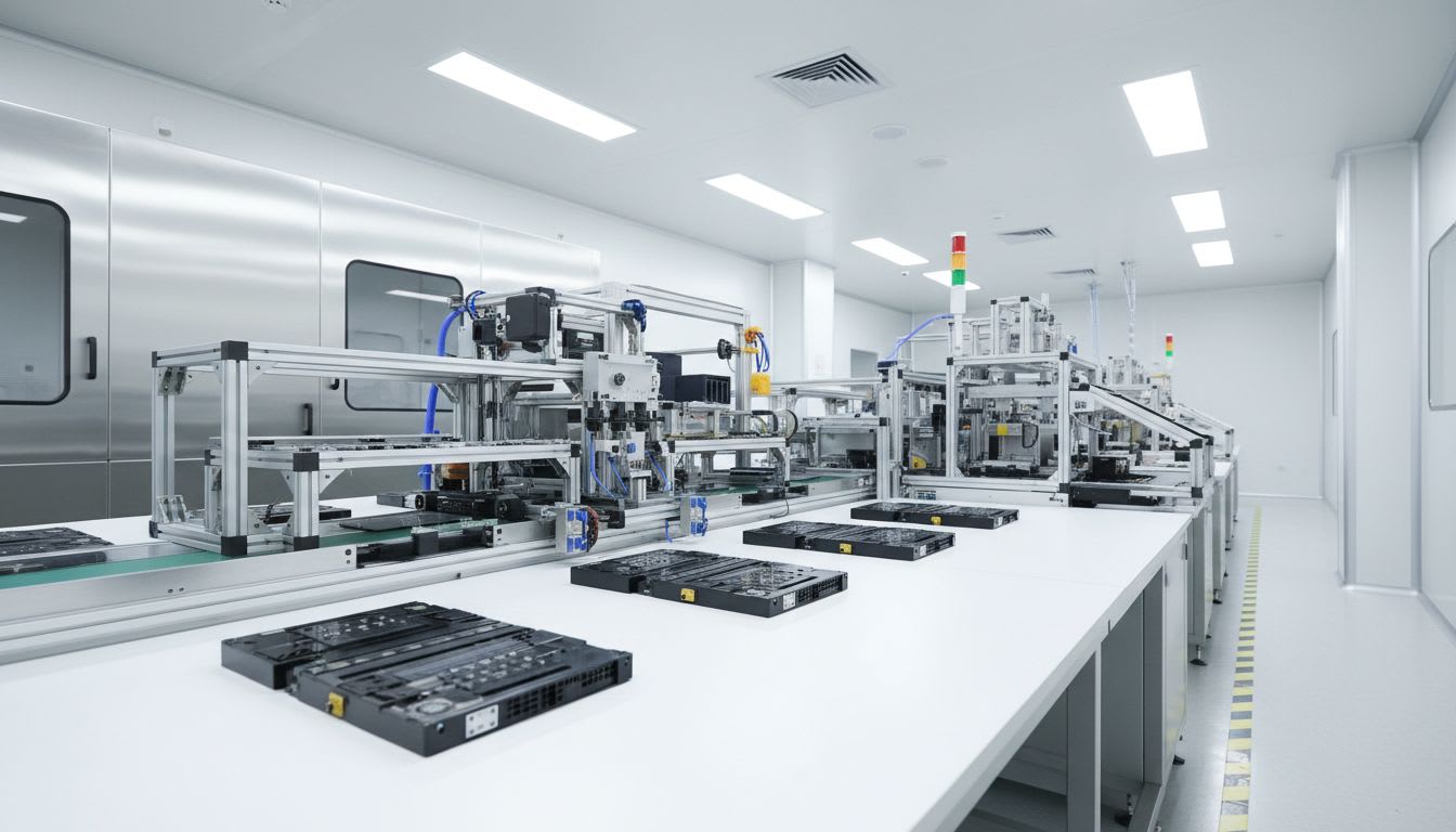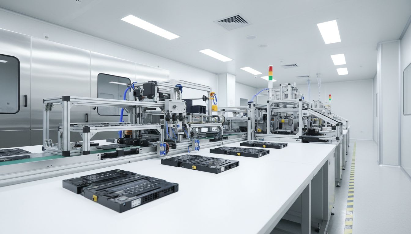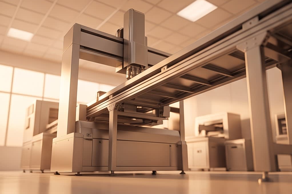

Just a few years ago, semiconductor cleaning was considered little more than the ‘finishing step’ of the process. However, as chip integration increases and package structures become more complex, precision processes such as cleaning, lamination, and grinding are emerging as key variables that determine final yield. In semiconductor manufacturing sites, the required precision level for these processes will continue to rise.
Why the Cleaning Process Is the Starting Point of Yield
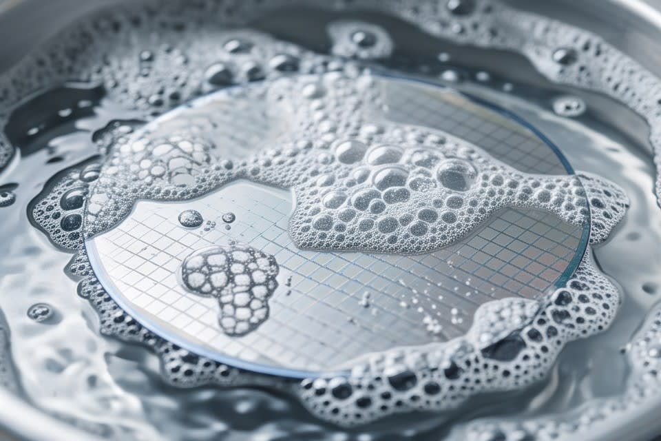
In semiconductor production lines, the seeds of defects grow where they cannot be seen. A single microscopic contaminant particle remaining on the surface of a wafer or tray can disrupt the yield of the entire subsequent process. This is exactly why cleaning is not simply ‘washing away’.
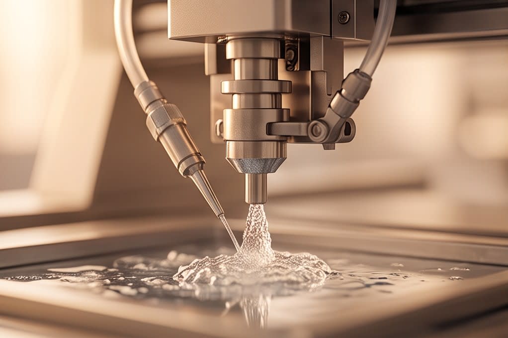
The micro nanobubble method, which generates fine bubbles of 0.1μm or smaller in water to remove organic matter, effectively separates contaminants while minimizing physical impact on the surface. The principle is that the localized pressure generated when bubbles collapse detaches particles from the surface. When a multi step configuration is added, using Water Jet to push away foreign matter and Air Knife to remove moisture, cleaning efficiency becomes significantly different compared to a single method.
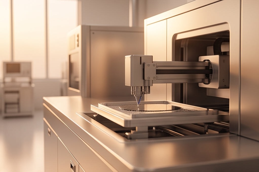
The more contamination sensitive the ultra precision components are, such as camera modules, autonomous driving sensors, and VCM motors, the more clearly the effect of this multi step cleaning appears. The Huvics Cleaner System is equipment configured to apply this multi step cleaning principle to actual mass production environments, and it is equipped with an Oven Dry function to handle the drying process as part of a single flow. This structure reduces the risk of recontamination that can occur when cleaning and drying are separated. Ultimately, the understanding is taking hold in manufacturing sites that cleaning is the starting point of the process and the foundation for quality in all later stages.
Why Precise Control in the Lamination Process Matters
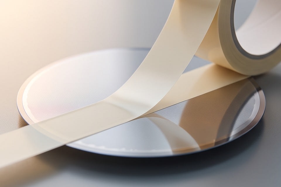
One of the defects that occurs most quietly yet critically in the lamination process is adhesive residue. UV curing tape operates on the principle that its adhesive strength decreases when exposed to ultraviolet light, making it easier to separate chips from the tape after dicing. The problem occurs when sufficient UV energy is not delivered. If curing is incomplete, adhesive remains on the chip surface, and this residue can become a contamination source in subsequent processes or affect electrical characteristics.
On the other hand, excessive UV exposure can cause thermal damage to the tape substrate or the chip itself, making the precision of energy control a key variable that determines process results. The same applies to adhesion uniformity in the Tape Mounting step. If the tape is not evenly attached, the chip can move slightly during dicing, reducing cutting precision.
The Huvics Laminator System processes the steps from Expander to Tape Mounting and UV Curing within a single system, and it is configured to selectively apply two UV methods: Lamp and LED. By integrating process steps, the key is to reduce condition fluctuations that can occur between each step and to maintain stable adhesive strength and curing quality.
In the Era of Stacked Packages, Grinding Precision Determines Performance
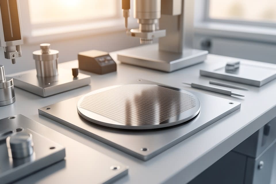
As stacked package technology, which stacks chips in multiple layers, becomes more advanced, requirements for thickness uniformity and surface flatness in each layer become stricter. Traditional bump based stacking structures created a gap of about 30μm between dies, but hybrid bonding, which directly connects copper to copper, reduces this gap to nearly 0. As the gap narrows, the allowable range of thickness variation in the grinding process also narrows.
In products that stack dozens of chips, such as AI semiconductors or high performance memory, accumulated thickness variation in one layer can collapse the flatness of the entire package, leading to electrical connection defects. The Huvics PKG Grinder is equipment that uses Diamond Wheel based micron level grinding to uniformly process packages to the thickness required by customers across various package types such as FCBGA, WLCSP, and QFN/DFN. It supports both Full Auto and Manual configurations, securing flexibility for production lines. As stacked structures become denser and packages become thinner, it will become even clearer in future technology competition that grinding precision is a condition that determines the performance and reliability of next generation semiconductors.

Cleaning, lamination, and grinding may appear to be independent processes, but these three steps are connected as one quality chain. Contamination in an earlier step disrupts precision in a later step, and subtle differences in curing conditions determine the reliability of the final chip. Preventing defects in semiconductor processes ultimately comes down to how tightly these invisible connections are managed.
Huvics is an advanced technology company that develops and manufactures automated equipment and
production systems across the semiconductor, LED, Mobile, and Cosmetic industries.
With top talent and continuous technological innovation, we support improved customer productivity and
secure quality competitiveness.
Huvics Contact
Phone: 031-374-8285
Email: cdpark@huvics.com