Just a few years ago, ‘micro contamination management’ in semiconductor processing used to focus primarily on specific key stages. However, recent advancements in circuit miniaturization and heightened yield demands have set rigid standards allowing no room for a single micro particle. Now, every moment—from wafer processing to cleaning and even material transfer—is recognized as a contamination-prone ‘critical moment.’ Amid these changes, Huvics emphasizes the importance of integrated solutions that go beyond mere equipment supply to block contamination risks across the entire process. Where should our semiconductor industry look for new solutions to reduce defect rates moving forward?
Micro Contamination Control in Grinding and Polishing Stages
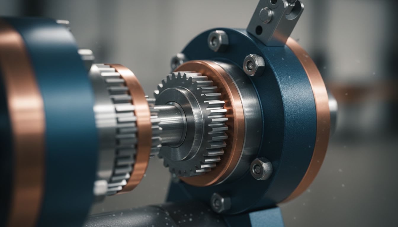
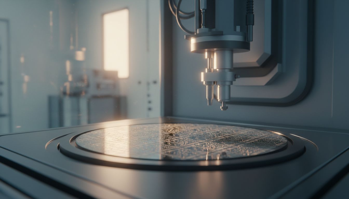
Everyone in the semiconductor industry agrees that even a small defect can lead to significant losses for the entire production line. The grinding and polishing stages, especially, where wafers or packages are processed to a specified thickness, inevitably involve mechanical friction and material removal, which can result in the mass generation of micro particles. These dust particles, barely visible to the naked eye, can cause critical defects such as shorts or functionality deterioration of micro circuits if they enter subsequent processes. Hence, the effectiveness of controlling contamination sources at this initial stage becomes crucial in determining the defect rate of the entire process. Huvics’ Grinder System and PKG Grinder dramatically minimize the occurrence of these contamination sources through ultra-precision grinding technology and micron-level precision machining capabilities. This not only involves material removal but also lays down a robust foundation for ensuring high-quality stability of the final product by reducing contamination risks from the beginning and guaranteeing the precise thickness and uniformity our clients require.
Residual Contamination Removal through Multistage Cleaning and Perfect Drying
Issues in Cleaning and Drying Processes
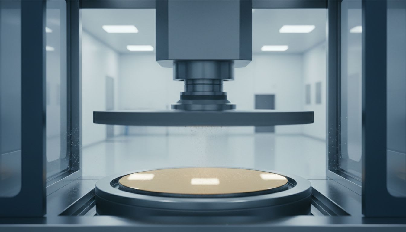
No matter how much contamination is reduced during the grinding and polishing process, micro particles are almost impossible to avoid completely. Therefore, a multistage cleaning technology that thoroughly removes residual contamination particles on the product surface right after processing is critical for the success of the next stages. The interface where drying occurs after wet cleaning is a particularly sensitive moment that can cause new contamination, thus requiring a perfect finish beyond simple cleaning. For instance, the following problems may arise:
- Residual chemicals can adversely affect subsequent processes
- Improper drying can result in watermarks forming on the surface
- Ambient micro particles can reattach during drying
Huvics’ Multistage Cleaning Technology
To address these fundamental contamination issues, Huvics’ Cleaner Machine employs the following multistage cleaning technologies to meticulously eliminate even the finest contamination particles from product surfaces.
- Micro bubble technology is used to effectively remove micro contamination particles
- Powerful water jet technology cleans residual contaminants from surfaces
- An air knife technology ensures complete drying and prevents reattachment
Oven Dry for Perfect Drying
Moreover, through a robust Oven Dry function, it thoroughly prevents watermarks or reattachment phenomena that can occur after cleaning, maximizing particle removal efficiency and firmly ensuring the quality stability of the final product.
Blocking Contamination Risks in Material Transfer and Handling Processes
Contamination Sources in Transfer and Handling Processes
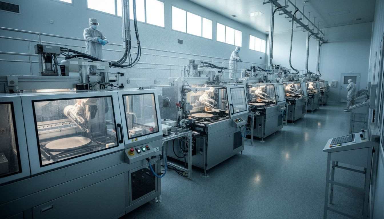
Another overlooked contamination vulnerability in semiconductor processing is the material transfer and handling process between process stages. Every moment that wafers or packages are moved from one piece of equipment to another, or during loading and unloading, they are inevitably exposed to the external environment. During this time, the following contamination sources can lead to critical defects in the final product:
- Invisible airborne micro particles ingress
- Contamination from minor contact by operators
- Contamination originating from the transfer trays or jigs themselves
Particularly if the transfer tools, which are supposed to be kept clean, contain contamination sources, then no matter how strictly the process stages are managed, it becomes futile.
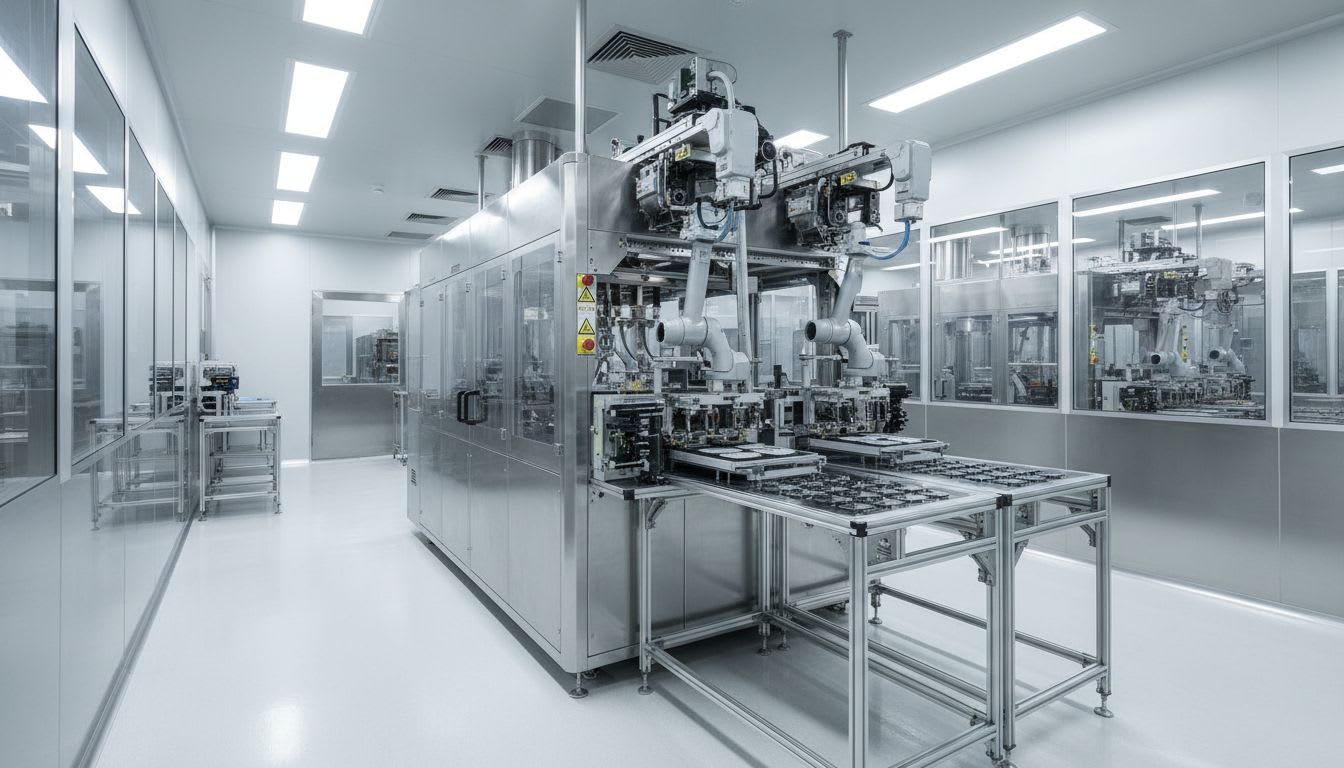
Automated Transfer System
With a deep understanding of these potential threats, Huvics plays a critical role in establishing a ‘fully automated transfer and clean handling protocol’ that surpasses mere process efficiency. Huvics’ Full Auto system minimizes contact with the external environment during material transfer between equipment and fundamentally eliminates the possibility of human error.
Cleaning and Drying of Transfer Tools
To thoroughly remove micro contamination particles that might remain on transfer trays or jigs, Huvics provides a Cleaner Machine featuring the following multistage cleaning technologies.
- The use of micro bubble technology effectively removes micro particles
- Powerful water jet technology cleans residual contaminants from surfaces
- The air knife technology ensures complete drying and prevents reattachment
This goes beyond simple cleaning to guarantee perfect drying through an Oven Dry function, fundamentally preventing the transfer tools from becoming contamination sources themselves.
Reducing Defect Rates with Huvics’ Integrated Contamination Management Solutions
To significantly reduce defect rates occurring in semiconductor processing, it is vital to clearly recognize and effectively control that micro contamination sources can threaten product stability throughout the entire process rather than just at specific stages. From this perspective, Huvics focuses on three contamination-prone key moments to actively support high-quality semiconductor production.
- Precisely controlling contamination sources in mechanical processing to minimize contamination risks.
- Perfectly removing residual contamination in the post-cleaning drying stage to prevent secondary contamination.
- Controlling the environment of the material transfer process and using automation to reduce recontamination risks.
In this way, Huvics ensures rigorous management from the start to the end of the semiconductor process, including even the inter-phase transfer stages, promising increased production efficiency and high product reliability for our clients.
Contamination management, which once focused on specific processes just a few years ago, now demands an integrated view encompassing the entire process. As we’ve explored today, every stage of semiconductor production—from wafer processing to post-cleaning drying and material transfer—carries potential contamination vulnerabilities. Huvics provides the essential solutions needed to protect the valuable productions of our clients against these invisible contamination sources, serving as a solid partner for the highest-quality semiconductor production. Ultimately, impeccable contamination control will be the crucial key determining the success of the future semiconductor industry.
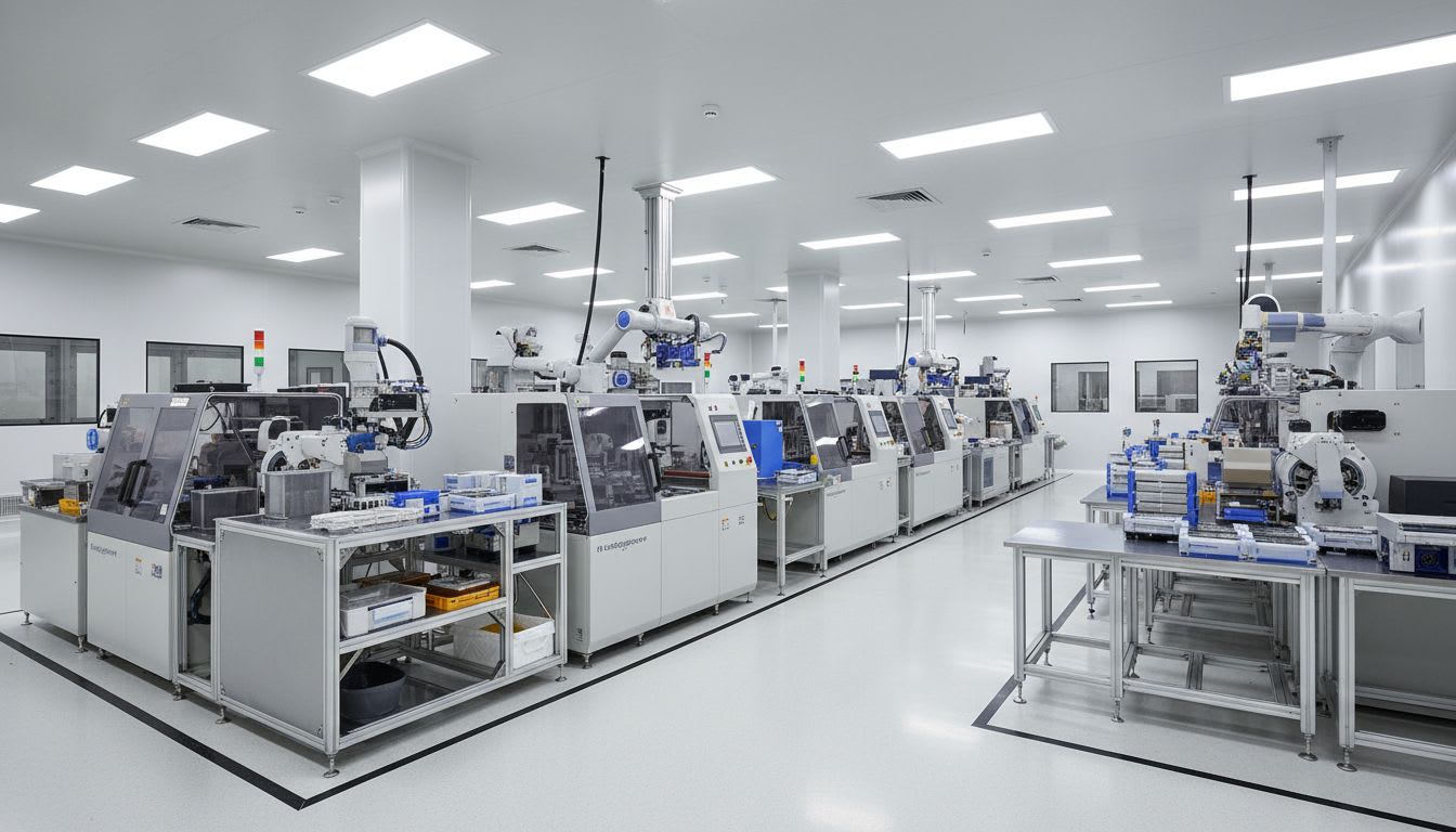
Huvics is a high-tech company developing and manufacturing automation equipment and production systems across semiconductor, LED, mobile, and cosmetic industries.
With top-tier personnel and continuous technological innovation, we support enhancing our customers’ productivity and securing quality competitiveness.
Huvics Co., Ltd. Contact
Phone: 031-374-8285
Email: cdpar&#k@huvics.com