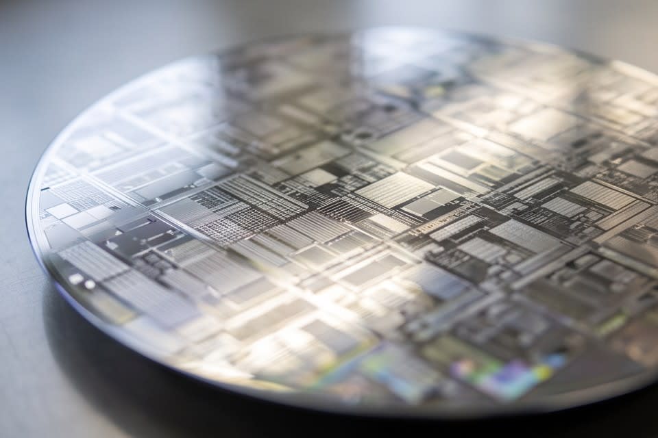
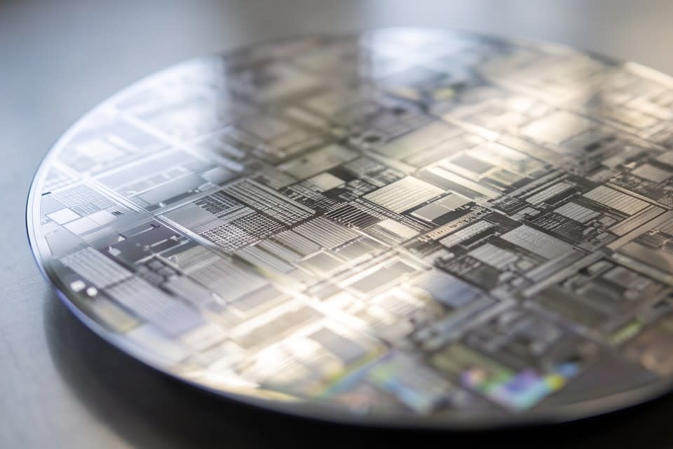
As the linewidths of circuits etched onto a single semiconductor chip have narrowed to the scale of just a few nanometers, the limits of acceptable contamination in the manufacturing process have also changed. In the past, it was enough to filter out foreign matter that was difficult to detect with the naked eye. Today, even a single fine particle floating in the air can become a variable that damages an entire circuit. As processes become more precise, the standards required of cleaning equipment have risen as well, and cleaning has become a core process that determines yield, not a final step for checking quality.
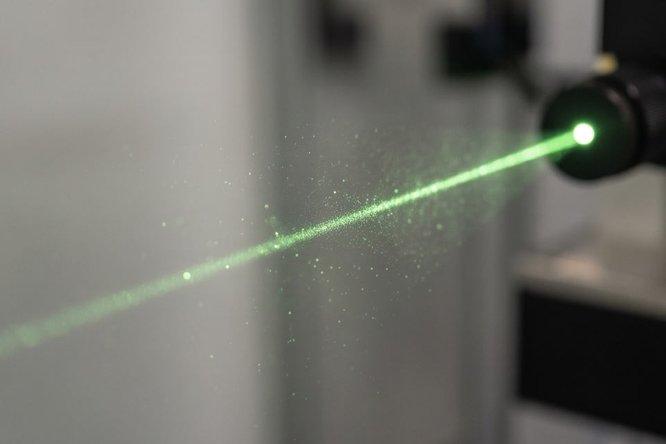
The structure in which particle contamination determines yield
In semiconductor processes, the impact of particle contamination on yield increases sharply as process generations advance. According to Applied Physics USA, in sub-10nm processes, aerosols measuring 0.1 to 0.5 micrometers are considered among the greatest risk factors, and even a single 10nm particle can cause a short circuit or structural deformation in a transistor.
The reality that even within the same production line, yield can vary between 95% and 75% depending on the level of particle contamination control shows that the cleaning process is not simply a matter of hygiene. As miniaturization progresses, the tolerance for contamination becomes narrower, and how precisely foreign matter is removed in the early stages of the process effectively determines the quality of the final product. This is why cleaning equipment is no longer a lower priority in process design, but has moved to the center of yield strategy.
As particle size becomes smaller, the precision required to detect and remove those particles also increases. Process miniaturization is changing the very criteria used to select equipment.
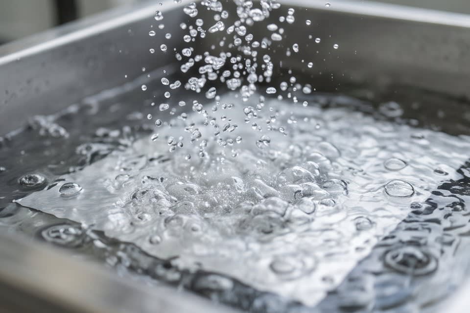
Principles and field application of multi stage cleaning technology
The performance of cleaning equipment depends on how contamination particles are separated from the surface. Micro bubble cleaning removes particles with shock waves generated when bubbles tens of micrometers in size collapse near the surface. In a study published in the Korean Journal of Chemical Engineering, a maximum jet flow velocity of 148.5mm/s was confirmed in a micro cylinder array structure, and this level of flow velocity is effective for removing fine contaminants with strong surface adhesion.
Nanobubble technology uses bubbles smaller than 5nm to reach even finer particles, and because the bubbles remain stable for a long time, cleaning efficiency is maintained even on complex surface structures.
Engineers handling components with different shapes in the field, such as camera modules, sensors, VCM motors, and trays, understand that it is difficult to process every product with a single method. This is why multi stage cleaning structures that combine Micro Bubble, Water Jet, and Air Knife are chosen for actual production lines.
The drying process, which completely removes residual moisture after cleaning, must also be integrated into a single flow to reduce the risk of foreign matter reattaching between processes. Designing cleaning and drying as one continuous system has become essential for securing quality stability.
Thickness uniformity and process integration determine defect rates
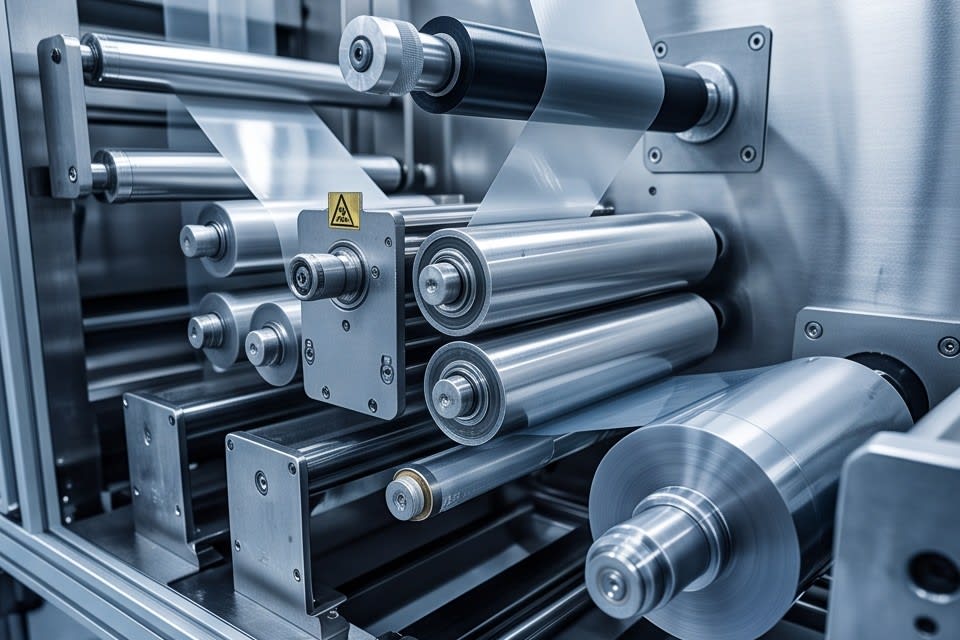
To reduce defects in the package processing stage, the first requirement is to clearly define the criteria for selecting equipment. The allowable range of total thickness variation, TTV, required in high performance packaging is typically 0.5 to 2.0 micrometers, and this standard becomes even stricter for products that stack chips in multiple layers, such as AI semiconductors and high performance memory.
Huvics takes an approach that structurally reduces defect factors occurring after cleaning through its PKG Grinder and Laminator System. The PKG Grinder uses a high precision stage and diamond wheel to uniformly process various packages, including FCBGA, WLCSP, QFN, and DFN, at the micron level, and its core role is to keep thickness variation within the allowable range. The Laminator System handles tape attachment and curing processes from Expander to UV Curing within a single line, reducing contamination and alignment errors that can occur during movement between processes.
Cases in which defects in semiconductor tape bonding processes or foreign matter issues in camera modules were resolved through cleaning and integrated process design show that equipment selection goes beyond simply comparing specifications. As stacking becomes deeper and package structures become more complex, thickness uniformity and process continuity act as the criteria that determine defect rates. The answer to what it means for final yield to reduce variables at a specific process stage is already embedded in the equipment design.
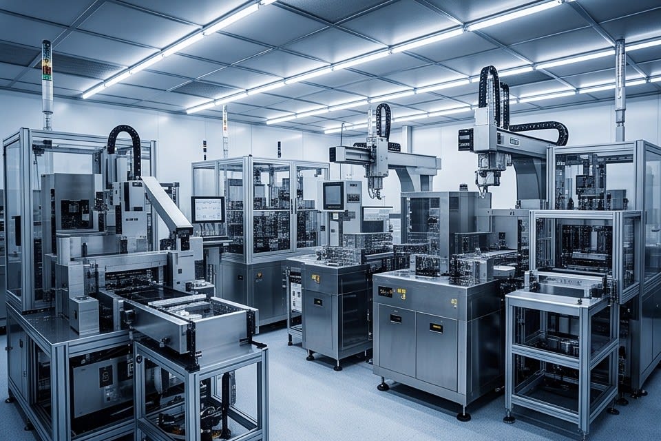
As semiconductor processes become more precise, the role of cleaning and processing equipment is shifting from simple support to the center of yield management. In an environment where the size of a single contamination particle can affect overall yield, the principle used to remove particles and the method used to control thickness variation become the practical standards for equipment selection. As the pace of process miniaturization accelerates, the importance of equipment that meets these standards will continue to grow.
Huvics is an advanced technology company that develops and manufactures automation equipment and
production systems across the semiconductor, LED, Mobile, and Cosmetic industries.
With top talent and continuous technological innovation, Huvics supports customers in improving productivity and
securing quality competitiveness.
Huvics Contact
Phone: 031-374-8285
Email: cdpark@huvics.com
