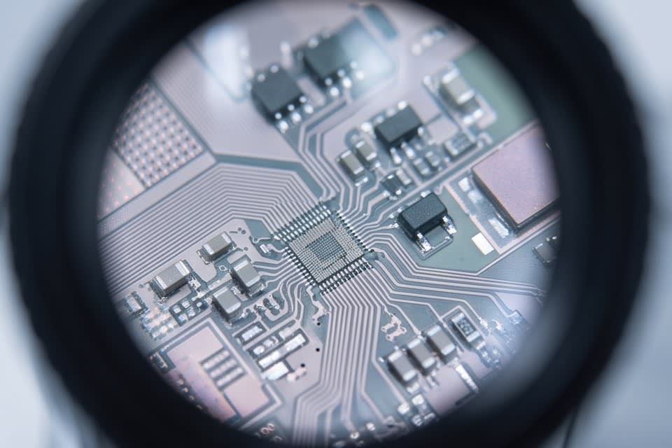
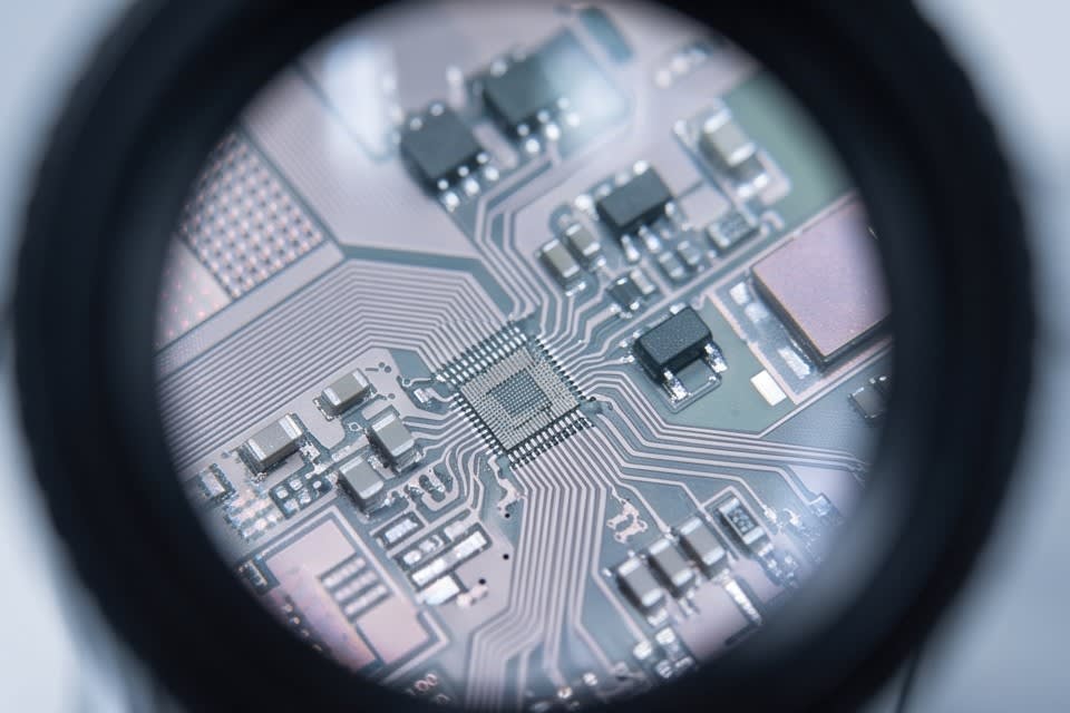
In semiconductor processes, it is not uncommon for a single defect to lead to the disposal of an entire finished product. According to an analysis by Elementary ML, automated optical inspection systems can achieve defect detection rates of up to 99.5%, while visual inspection remains at a maximum of around 80%, allowing 20% of actual defects to pass through the process unchecked. This figure is not simply a comparison of performance. It is a signal that the choice of inspection method directly determines competitiveness. In semiconductor manufacturing, where precision determines yield and cost, the question of how inspection is performed carries far greater weight than it may seem.
Limitations of Visual Inspection and the Need for Automated Inspection
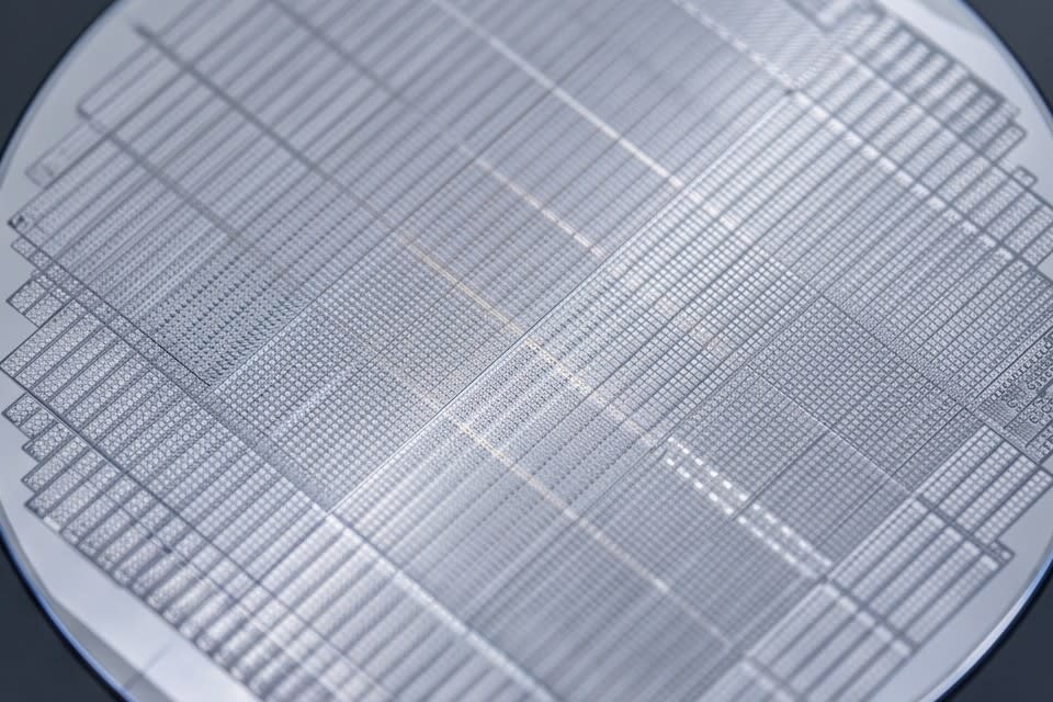
In semiconductor manufacturing processes, fine particle contamination becomes more critical as feature sizes shrink. According to patents registered with the United States Patent and Trademark Office (USPTO), contamination standards are so strict that even particles as small as 5 nanometers (nm) are not acceptable in many semiconductor manufacturing processes. However, visual inspection has structural limitations in identifying contamination at this microscopic level.
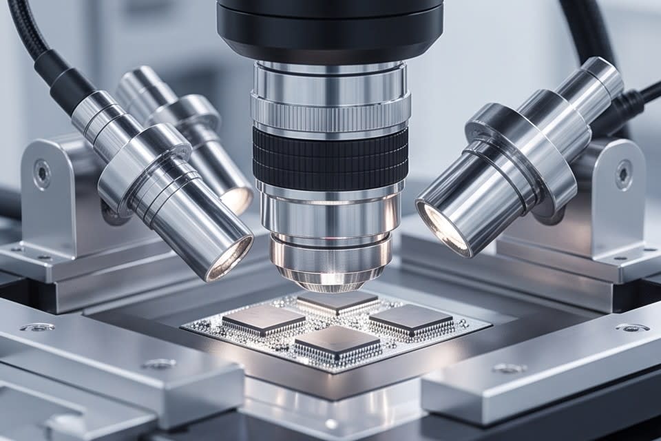
As confirmed in Instrumental’s 2024 analysis, the detection rate of visual inspection reaches only up to 80%. This means that one out of every five actual defects passes inspection. In contrast, automated optical inspection systems achieve detection rates of up to 99.5%, allowing algorithms to cover areas that the human eye can miss.
The gap between the two methods is not merely a difference in accuracy. Given the nature of semiconductor manufacturing, where the cost of detecting defects rises exponentially in later process stages, the choice of inspection timing and method becomes a variable that changes the entire yield structure. As miniaturization continues to accelerate, the need for an inspection system that does not miss even a single particle is becoming clearer. Industry standards themselves are shifting toward automated inspection, which meets the precision requirements that visual inspection can no longer handle.
Integrating Cleaning and Vision Inspection into One Flow
Operating cleaning and inspection as separate processes has a blind spot. When inspection is performed after cleaning is completed, secondary contamination generated during cleaning or particles that were not fully removed may be missed. One approach to solving this issue is to integrate the cleaning process and vision inspection algorithms into a single flow.
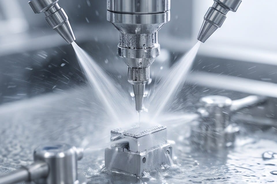
Huvics cleaner systems combine multi-stage cleaning technologies such as microbubble, water jet, and air knife to remove contamination particles from product surfaces step by step. Vision inspection algorithms are integrated into this process to automatically determine surface conditions before and after cleaning. For various components with different shapes and materials, including camera modules, sensors, VCM motors, and trays, the algorithm analyzes surface images and numerically evaluates residual contamination and cleaning quality. This approach does not rely on subjective operator judgment, and creates a structure that maintains consistent quality standards within the process.
Ultrasonic dispersion technology plays the role of uniformly dispersing contamination particles within the cleaning solution, while the vision algorithm verifies the result, making the two technologies complementary. As cleaning efficiency improves, the number of defects that inspection must filter decreases. As inspection accuracy improves, cleaning process standards can be adjusted more precisely. When cleaning and inspection form a feedback loop, overall process quality stability is implemented in a structure that improves step by step.
The Role of Vision Inspection Algorithms Confirmed in the Field
Huvics has confirmed through multiple field cases how the combination of vision inspection algorithms and cleaning technology changes actual defect rates in MLCC and FPCB processes.
In the semiconductor tape bonding process, residual foreign matter after tape attachment repeatedly led to bonding defects. By linking vision inspection algorithms with the cleaning process and automatically determining surface conditions before bonding, the point at which defects were identified was moved to the early stage of the process. In camera module processes, microscopic foreign matter between the lens and image sensor was a major cause of finished product defects, and there are accumulated cases showing that solutions combining ultra-precision cleaning with algorithm-based inspection have led to reduced defect rates.
In both cases, the cause of defects was hidden in a specific stage within the process, and the judgment criteria of the inspection algorithm played a decisive role in identifying it. In the MLCC process, ultrasonic dispersion technology suppressed the reattachment of contamination particles in the cleaning solution, while vision inspection quantitatively verified surface uniformity, improving the reproducibility of process quality.
In any process, defect patterns repeat. Algorithms learn those repetitions as data and refine their judgment criteria. These field cases show that the combination of precision cleaning and vision inspection is not simply a combination of technologies, but an approach that changes the quality structure across the entire process.
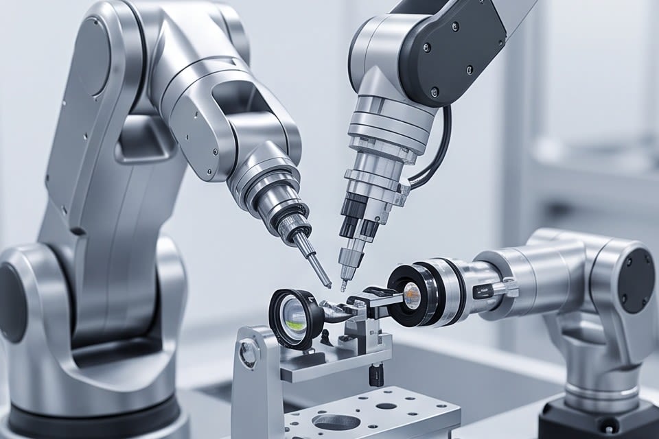
There is a fundamental difference between a product passing inspection after cleaning is completed and inspection verifying cleaning completeness in real time. Reducing defect rates ultimately depends on when and by what standards a decision is made, and vision inspection algorithms are a means of bringing those standards into the process. When precision cleaning and algorithm-based inspection are connected into one flow, defects are filtered not at the end of the process, but within the process itself.
Huvics is an advanced technology company that develops and manufactures automated equipment and
production systems across the semiconductor, LED, Mobile, and Cosmetic industries.
With top-tier talent and continuous technological innovation, we support customers in improving productivity and
securing quality competitiveness.
Huvics Contact
Tel: 031-374-8285
Email: cdpark@huvics.com



