The semiconductor cleaning process is a critical stage that determines the initial quality of products on the production line. It is not simply a matter of wiping a surface, but a technical process that precisely removes invisible fine particles and contaminants according to process conditions. When cleaning lens sheets before camera module assembly, or when removing foreign matter to reuse semiconductor trays, this process is often the first barrier field engineers encounter. The cleaning method can change yield and even shift the flow of the entire line.
Process challenges caused by diverse contamination types
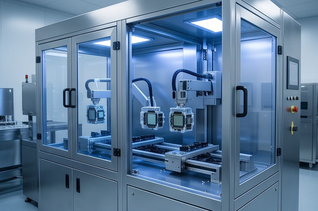
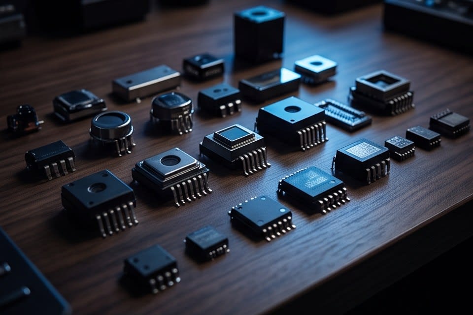
The first factor that makes the semiconductor cleaning process difficult is the diversity of contamination particles. When the cleaning target changes, such as trays, camera modules, sensors, and VCM motors, surface characteristics also change, and the size and wettability of the contaminants that must be removed vary widely. A single cleaning method cannot easily handle this diversity.
Some particles cannot be removed by physical impact alone, while some contaminants will not detach from the surface without chemical dissolution. As semiconductor processes become more miniaturized, allowable tolerances become narrower, while contamination types become even more complex. This is why cleaning in high precision processes cannot be solved by a single standalone technology.
Because failure in the cleaning stage affects the entire subsequent process, deciding which mechanisms to combine and in what order becomes a key criterion in process design. In the field, the approach of first identifying contamination characteristics and then selecting the cleaning technology suited to them is increasingly becoming the standard.
How multistage cleaning combinations solve these challenges
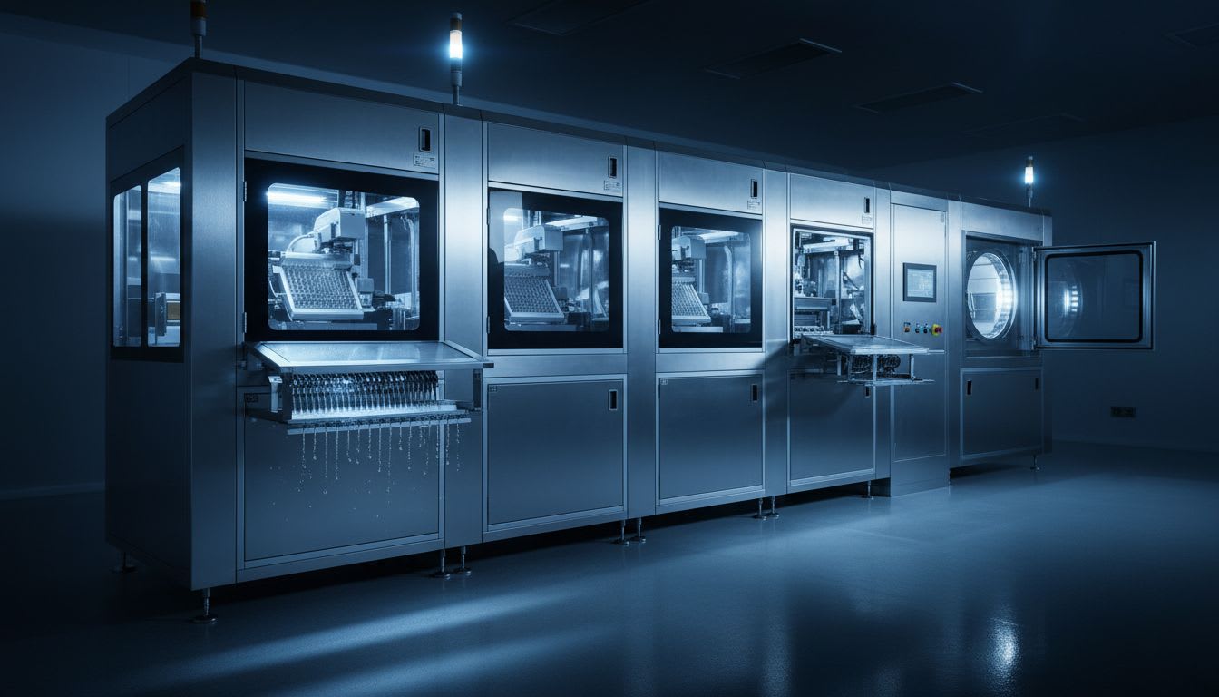
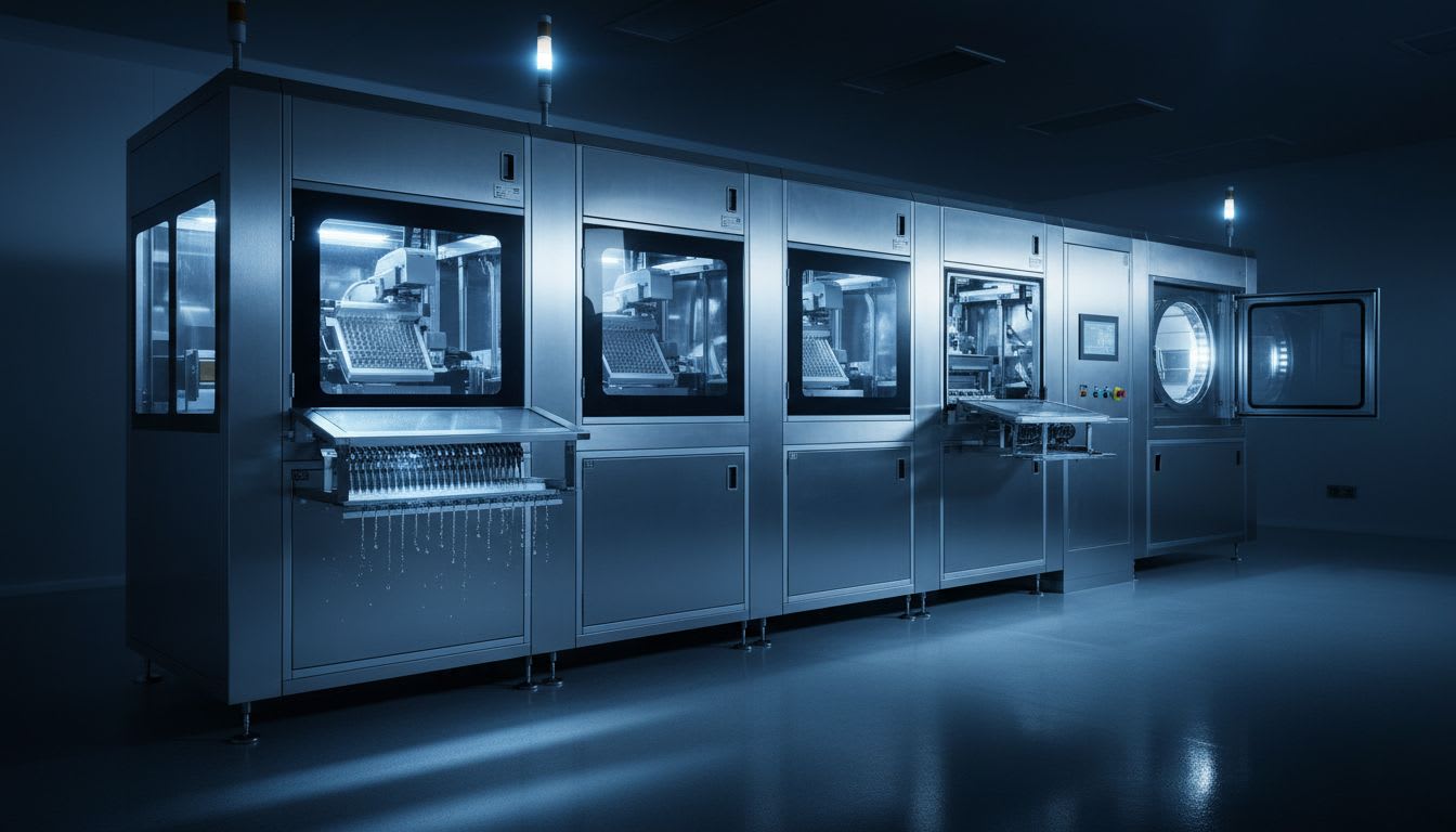
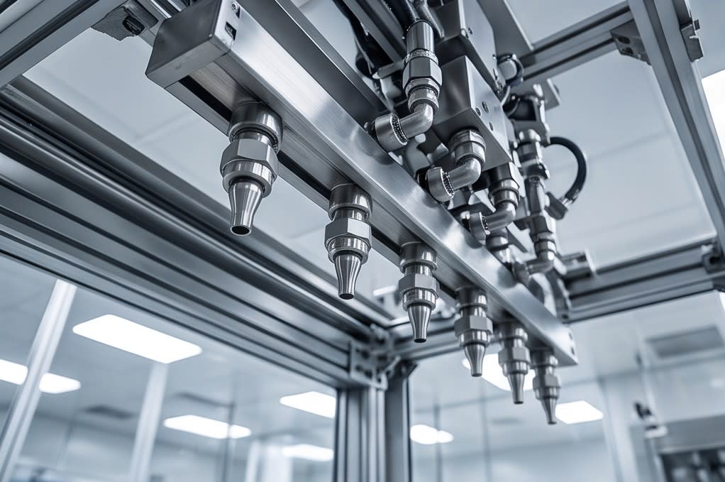
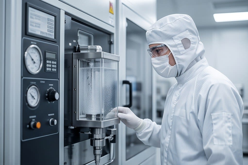
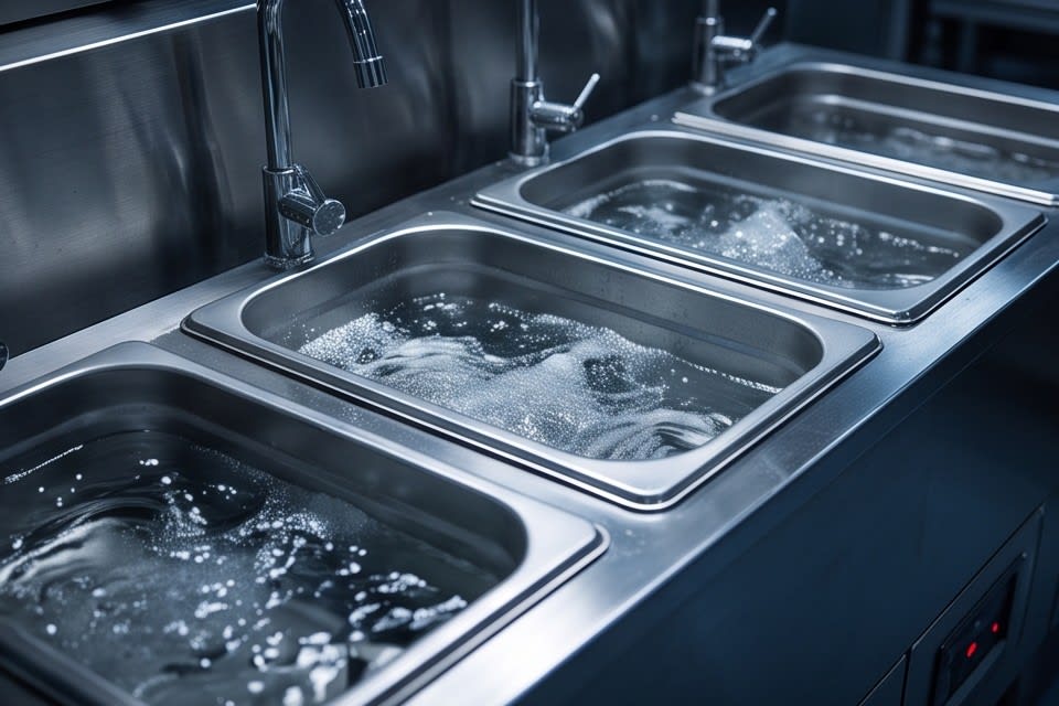
Multistage cleaning systems are gaining attention because they overcome the limits of a single technology through process combinations. Microbubbles use both chemical and physical effects, combining the oxidation reaction of the cleaning solution with the collapse impact of fine bubbles to remove surface contamination. When Water Jet is added to physically push away particles, followed by Air Knife to remove residual moisture, each stage is structured to compensate for the weaknesses of the others.
According to a study published in the Korean Journal of Chemical Engineering, an acoustic bubble array based cleaning device achieved up to 92.5% cleaning efficiency on semiconductor wafers. The drying stage after cleaning also needs to be designed as an integrated flow rather than a separate process to prevent secondary contamination caused by residual moisture. The Cleaner System from Huvics, which combines oven drying with this multistage configuration, is designed to handle everything from cleaning to drying within a single line.
When particle removal efficiency improves, the defect rate decreases, and when the defect rate decreases, the stability of the entire process is secured. Ultimately, which technologies are combined and how many stages are used become the key factors that determine the quality level of the cleaning process.
Why integrated equipment is needed for tray cleaning and grinding precision
Field challenges in semiconductor tray cleaning
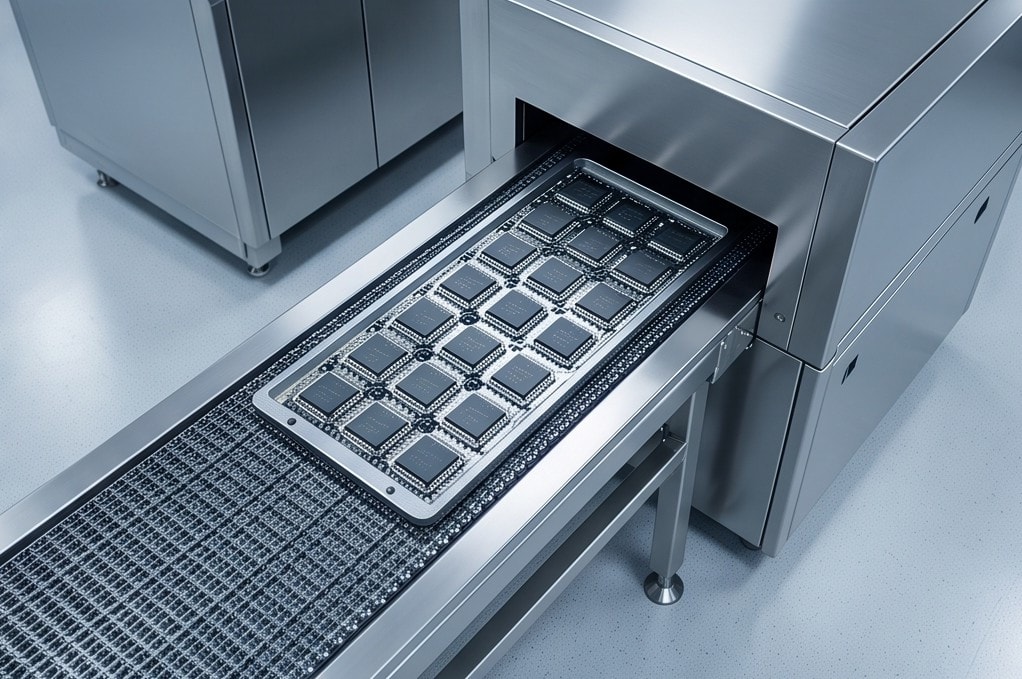
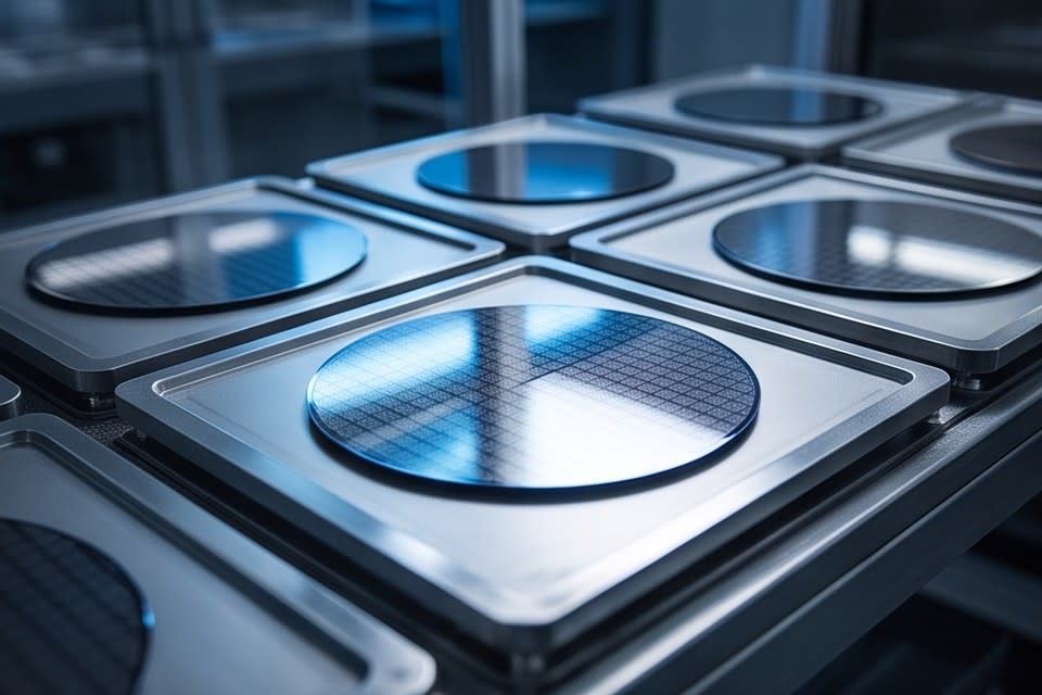
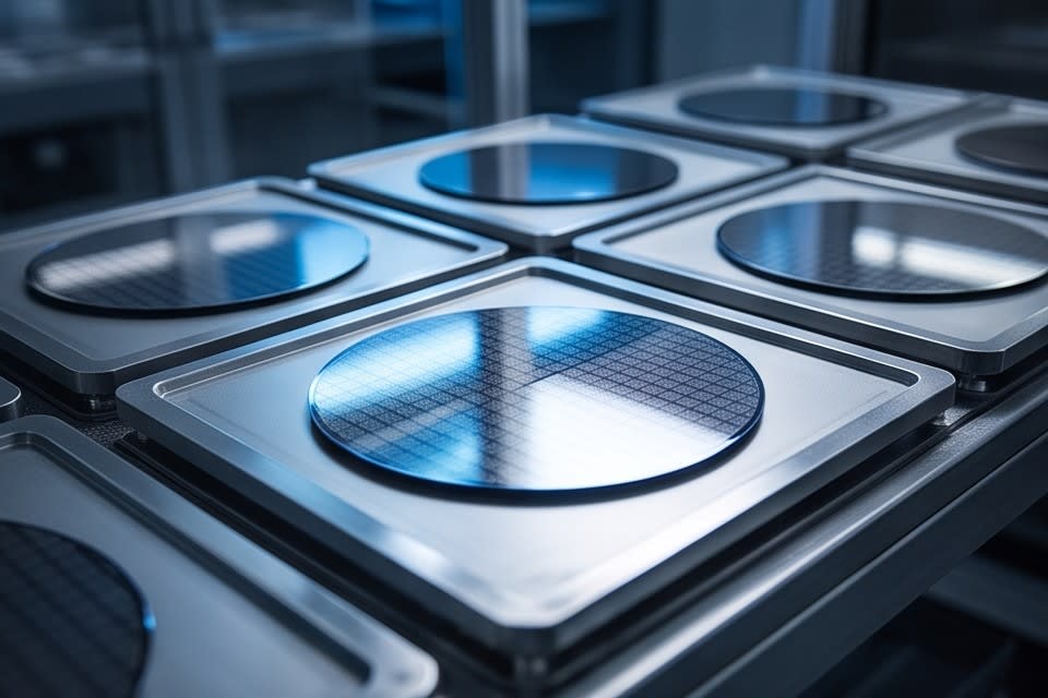
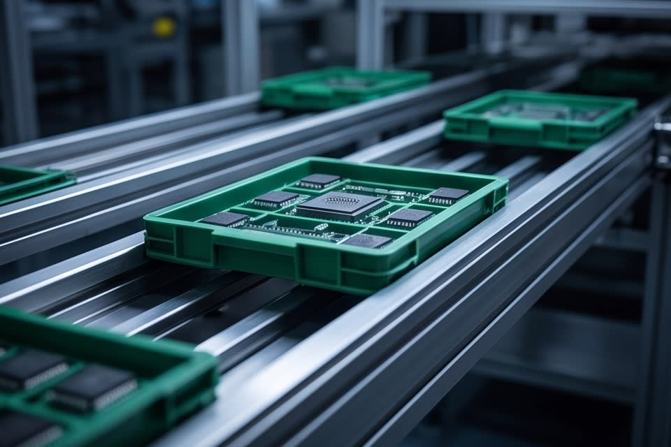
Semiconductor tray cleaning is one of the challenges that repeatedly appears in the field. Fine foreign matter remaining on the tray surface can cause contact defects or contamination during the chip loading process, which may lead to reduced yield across the entire line. Automated tray cleaning systems are known to process approximately 30,000 units per day, and to maintain this throughput reliably, equipment design must secure both cleaning quality and speed at the same time.
The meaning of grinding precision in package processes
Along with cleaning issues, grinding precision also serves as a key variable in semiconductor package processes. Each package type, such as FCBGA, WLCSP, and QFN·DFN, requires different thickness specifications, and tolerances for uniformity and flatness are becoming increasingly narrow. The PKG Grinder from Huvics uses a high precision stage and diamond wheel to achieve micron level thickness processing, and it can be configured selectively as Full Auto or Manual Type, allowing flexible application according to production line conditions.
Cleaning and grinding may appear to be separate issues, but the value of integrated equipment becomes clear when approached from the perspective that both processes are early stages that determine the final reliability of the package.
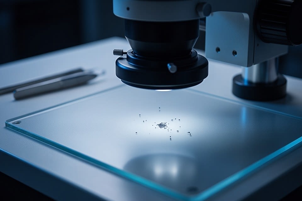
The challenges of the semiconductor cleaning process begin with the diversity of contamination types and the fact that process conditions differ by product. Multistage combinations rather than a single technology, integrated design of cleaning and drying, and integrated equipment configurations that also include grinding precision are becoming practical solutions in the field. No matter what process challenge you face, the starting point of equipment design is to accurately understand the nature of the contamination.
Huvics is an advanced technology company that develops and manufactures automation equipment and
production systems across the semiconductor, LED, Mobile, and Cosmetic industries.
With top tier talent and continuous technological innovation, we support customers in improving productivity and
securing quality competitiveness.
Huvics Contact
Phone: 031-374-8285
Email: cdpark@huvics.com