

When I first took a close look at a semiconductor package process site, the customers I met all said something similar. “We changed the equipment and the materials, but we still do not know why defects are not decreasing.” What we commonly found at those sites was an issue that was hard to see with the naked eye: micron-level thickness variation and contamination particles left between process steps. Processes that appeared normal on the surface were quietly reducing yield at each stage as they accumulated and connected.

Why thickness variation determines yield
AI semiconductors and high-performance memory semiconductors improve performance by vertically stacking dozens of chips. In this structure, if the thickness of each die is not uniform, alignment shifts during stacking, stress concentrates at the bonding area, and errors eventually occur in electrical signal transmission.
According to analysis by Applied Materials, today’s HBM dies have become about one twenty-fifth the thickness of conventional DRAM, making them highly vulnerable to stress, warpage, and deformation. In addition, research published by ASME clearly shows that thickness variation and alignment mismatch worsen performance variation in HBM multi-layer stacking.
As the number of stacked layers increases from 12 to 16 or more, these mechanical issues become intertwined in complex ways, increasing the risk of bonding defects and yield loss. Ultimately, package thickness control is not simply a dimensional matter but a key variable that determines the electrical performance and reliability of a product. As stacking increases, variation accumulates with it, and that error appears directly in the final yield. This is exactly why micron-level precision is required, and this trend becomes even clearer as next-generation packaging technology advances.

The direction of yield is set in the grinding stage
PKG Grinder combines a high-precision stage with a diamond wheel to uniformly grind various packages such as FCBGA, WLCSP, QFN, and DFN to the customer-required thickness at the micron level. The key challenge this equipment addresses is achieving both speed and precision at the same time.
Even in high-speed processes, thickness variation must be minimized to maintain yield, and the same level of precision must be guaranteed even when package types change to secure the stability of the entire production line. Since it supports both fully automated and manual operation, it can flexibly respond from low-volume, high-mix production to high-volume continuous processes.
The grinding process is positioned to determine the quality of subsequent stacking and bonding in advance. Only dies with uniform thickness enable accurate alignment and stable bonding in the next process. The key point of this process is that yield is not created in the assembly stage, but its direction is already set in the grinding stage.

Contamination control that connects every process stage
Process continuity from lamination to UV curing
If thickness control is an issue before stacking, contamination control throughout the entire process is another axis of equal importance. In semiconductor package manufacturing, a process that connects lamination, tape mounting, and UV curing into one flow must consistently maintain adhesive strength and alignment accuracy between each step. If the process is interrupted or conditions change, quality variation occurs at that point.
Multi-stage cleaning and static electricity suppression
The same applies to the cleaning process. A multi-stage cleaning method that sequentially applies microbubbles, water jets, and air knives removes surface contamination particles step by step, while also implementing a principle that suppresses particle reattachment caused by static electricity between stages. To apply the same cleaning standards to components with different shapes and materials, such as camera modules, sensors, VCM motors, and trays, process conditions must be finely adjusted.
In a reality where a single particle can be judged as a defect in the final inspection, cleaning is not the final finishing step but the point where quality begins. The Huvics Cleaner System integrates even oven drying functions to block additional contamination risks caused by residual moisture after cleaning. The fact that yield stability is maintained across the entire process only when contamination is controlled at every connection point is confirmed in actual production sites.
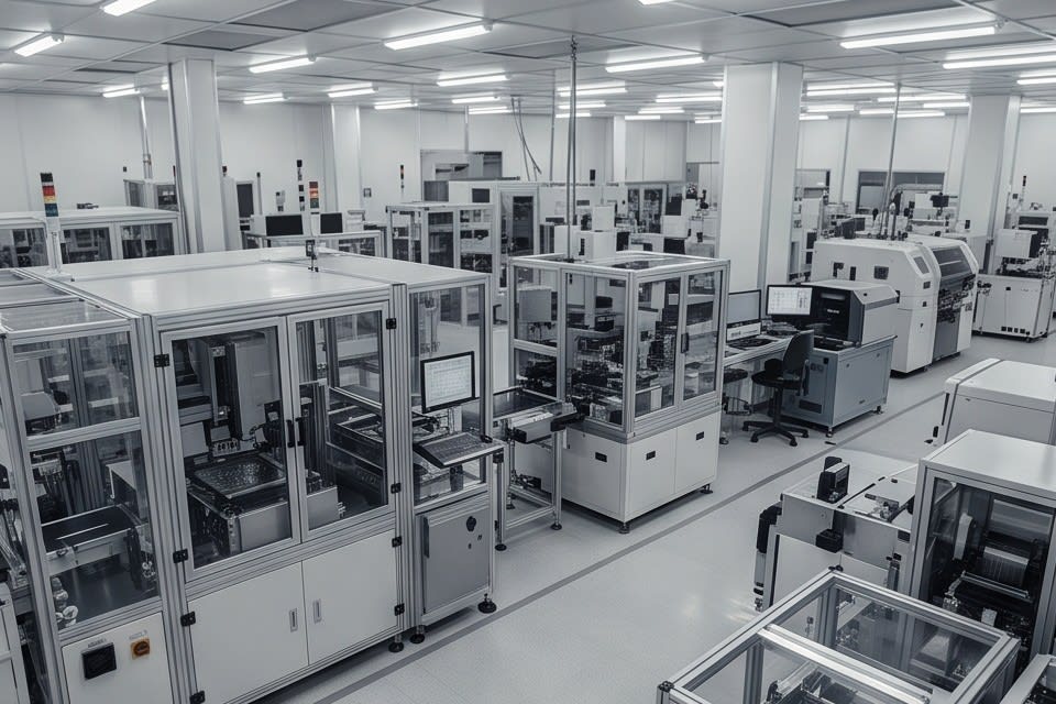
The frustration customers first expressed, the question “Why does it still not work after changing everything,” was ultimately answered in places that are not visible. Micron-level thickness variation, a single particle left between processes. Semiconductor quality control is not about replacing visible equipment, but about building precision at every connection point between processes. From grinding to cleaning, yield finally appears as a number when that flow is maintained consistently.
Huvics is an advanced technology company that develops and manufactures automation equipment and
production systems across the semiconductor, LED, Mobile, and Cosmetic industries.
With top talent and continuous technological innovation, we support customers in improving productivity and
securing quality competitiveness.
Huvics Contact Information
Phone: 031-374-8285
Email: cdpark@huvics.com
