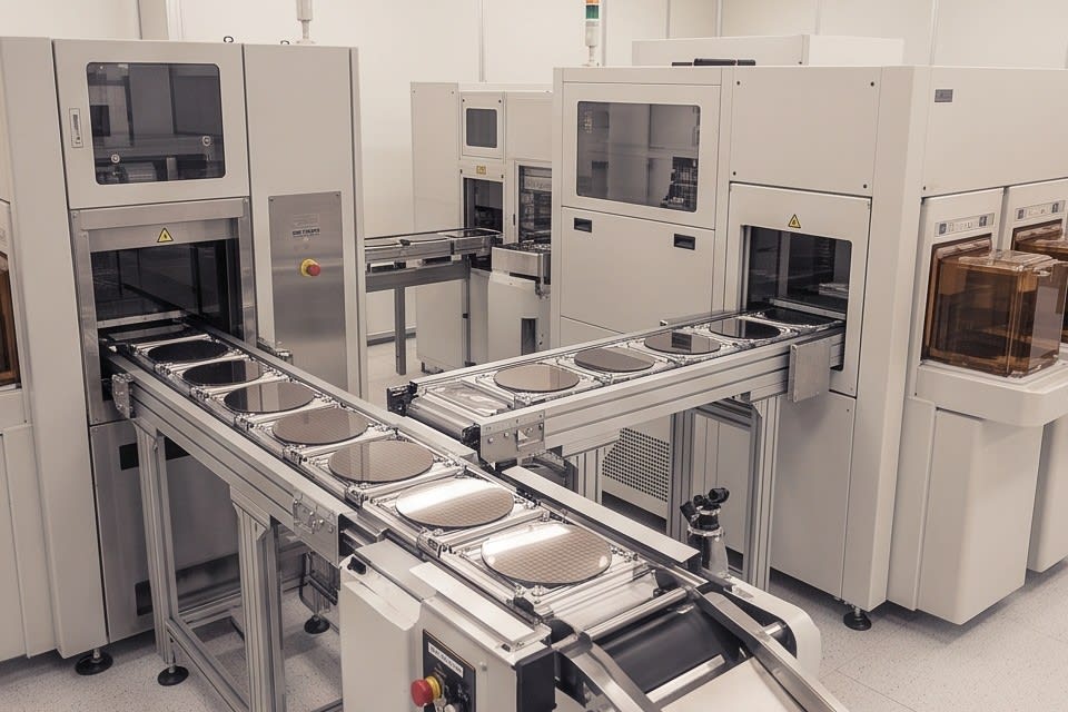

To reduce defect rates in semiconductor processes, many manufacturers have focused on improving the precision of individual equipment. Typical approaches include adopting more sophisticated stencils and faster inspection equipment. However, even when the performance of each piece of equipment is enhanced, contamination and alignment errors that occur during transfer between processes still hold back yield. It is now time for an integrated design perspective that connects the entire process into one continuous flow.

Why tape attachment and UV curing determine stacked packaging quality
In stacked semiconductor packaging, tape attachment and UV curing are not simply auxiliary material processes. The entire sequence from fixing chips onto the wafer to peeling them accurately after dicing depends on these two steps.
UV curing technology creates immediate adhesion and high tensile strength the moment ultraviolet light activates the photoinitiator inside the adhesive. When ultraviolet light is applied again afterward, adhesion decreases, allowing the chip to be removed cleanly from the tape. If this precise control of adhesion and peeling is not achieved, residual adhesive may remain on the chip surface or microcracks may occur during peeling.
Especially in ultra-fine packages with a pitch level of 0.3~0.4mm, placement alignment errors must be controlled within several tens of micrometers, and variations in curing timing and intensity lead directly to process defects. As stacked structures become more complex, requirements for thickness uniformity and flatness of each layer also increase.
Because even slight variations that occur during the tape attachment stage are amplified later in grinding or dicing processes, the stability of the initial adhesion process becomes the baseline for overall yield. Ultimately, maintaining consistent UV exposure uniformity and adhesive strength is the key to stacked packaging quality.

How an integrated laminator structure enhances process quality
Problems that arise when process equipment is operated separately often come not from the performance of the equipment itself, but from the sections between equipment. Every time a wafer or substrate moves from the expander to the tape mounter and then to the UV curing equipment, the possibility of foreign particle inflow and alignment deviation arises. For process managers, the parameters of each piece of equipment must be managed separately, and it is also difficult to identify at which stage a problem that occurred during transfer originated.
As the number of transfers decreases, contamination contact points are reduced and continuity of conditions between processes is secured. For this reason, one-stop laminator structures that handle everything from expanding to UV curing within a single system are gaining attention.
The Huvics laminator system integrates lamination, tape mounting, and UV curing into one flow to reduce quality variables that occur during transfer between processes, while its UV curing system supporting both lamp and LED methods secures adhesive strength and process stability together. With both semi-auto and manual options, it flexibly supports everything from high-mix, low-volume production to mass production lines.
By simplifying the process, takt time is reduced, and a workflow that eliminates bottlenecks is becoming established on manufacturing floors.

Why the cleaning process determines final yield
The cleaning process is often regarded as a finishing step that wipes the surface after assembly is completed, but in reality, it is closer to the starting point that determines final quality stability. Contaminant particles only a few micrometers in size remaining on the semiconductor surface can cause poor electrical contact or degraded optical characteristics, which directly leads to yield loss.
According to industry analysis, a 1% increase in yield in semiconductor manufacturing can generate an estimated additional net profit of about 150 million dollars, showing that the economic impact created by differences in cleaning efficiency is significant.
The Huvics cleaner system uses a multi-stage cleaning method that combines micro bubbles, water jet, and air knife to remove contaminant particles from product surfaces step by step. It optimizes cleaning conditions for products with diverse shapes and materials, such as camera modules, sensors, VCM motors, and trays, and is equipped with an oven drying function to completely remove residual moisture after cleaning. Users can choose between full-auto and manual methods depending on line conditions, allowing flexible response to both process automation and maintenance.
As particle removal efficiency increases, defect rates decrease, and the rework ratio in subsequent inspection processes is also reduced through a chain effect. Only when cleaning is complete does the entire process close, and its meaning is confirmed in the final shipment quality figures.

In semiconductor processes, quality depends not on the performance of any single piece of equipment, but on how tightly each process is connected to the next. Only when the precision of tape attachment, the uniformity of UV curing, and the completeness of cleaning each perform their roles can the yield curve become stable. Reducing gaps between separated equipment and designing the process flow as one connected system is the direction that manufacturing sites need today.
Huvics is an advanced technology company that develops and manufactures automation equipment and
production systems across the semiconductor, LED, Mobile, and Cosmetic industries.
With top talent and continuous technological innovation, Huvics helps customers improve productivity and
secure quality competitiveness.
Huvics Contact Information
Phone: 031-374-8285
Email: cdpark@huvics.com
