
Tag: process automation

  • Precision Cleaning and Process Automation Solutions That Determine Semiconductor Wafer Yield: Analysis of Huvics Technology

    Precision Cleaning and Process Automation Solutions That Determine Semiconductor Wafer Yield: Analysis of Huvics Technology

    Huvics

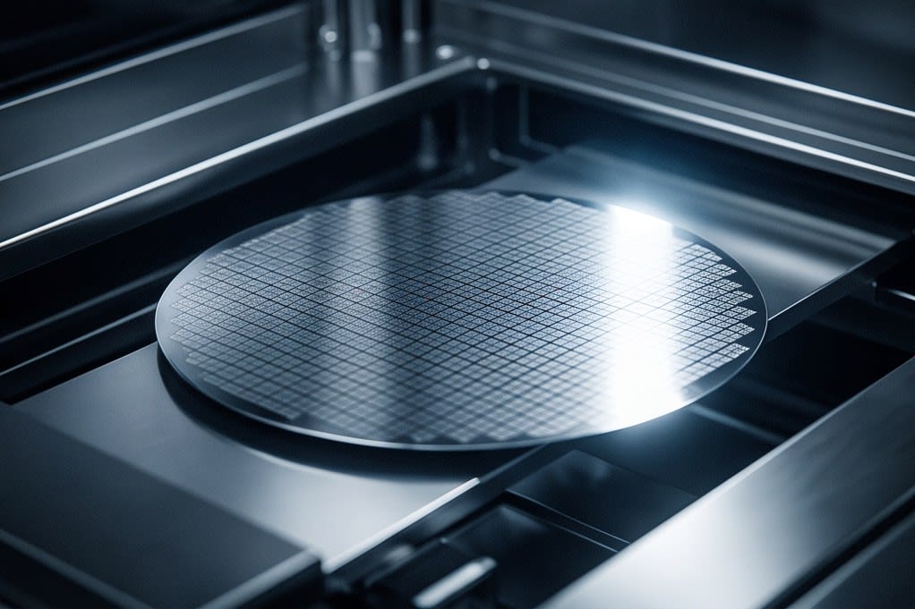
    In semiconductor manufacturing, even a microscopic residue invisible to the eye can become the trigger for a major defect. Today, as nanoscale precision processes have become standard, the cleanliness of the wafer surface is more than just one step in the process. It is a key indicator that determines the final product yield. Because such micro contamination directly leads to significant cost losses for companies, thorough and flawless surface management has now become a strategic necessity rather than an option.

    Based in Osan, Gyeonggi-do, Huvics is a group of specialists that has transformed deep challenges from the field into technical solutions, from semiconductor tape bonding processes to tray cleaning technology. Let us take a closer look at the core of the innovative process design Huvics offers for your journey to maximize production yield through precision cleaning and process automation.
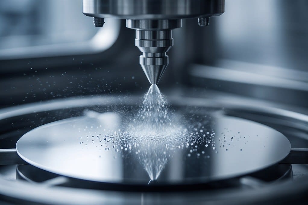
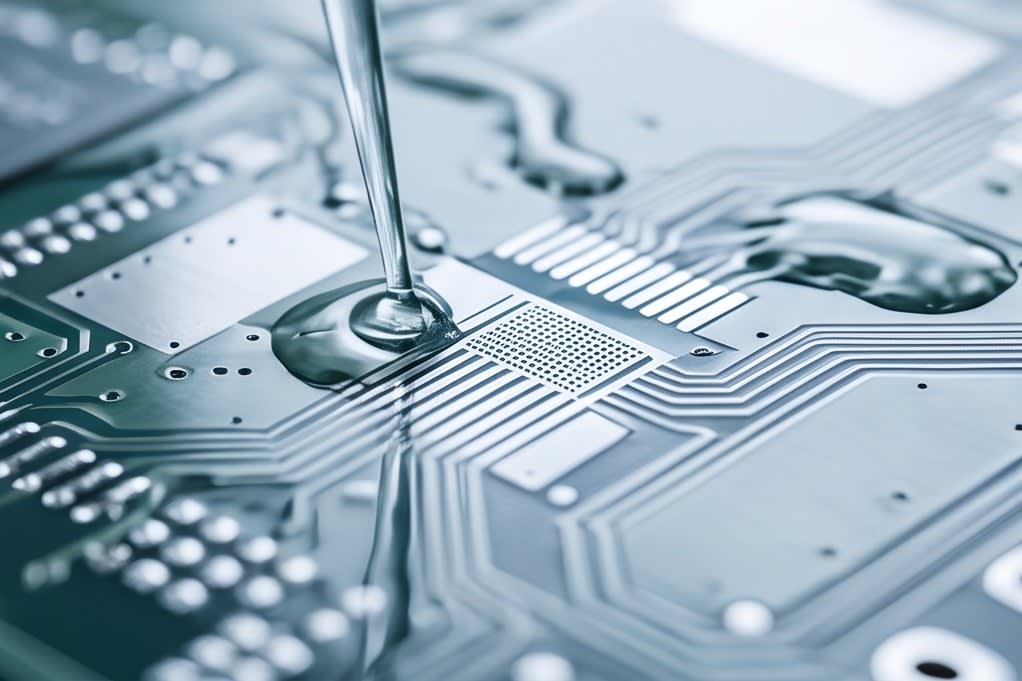
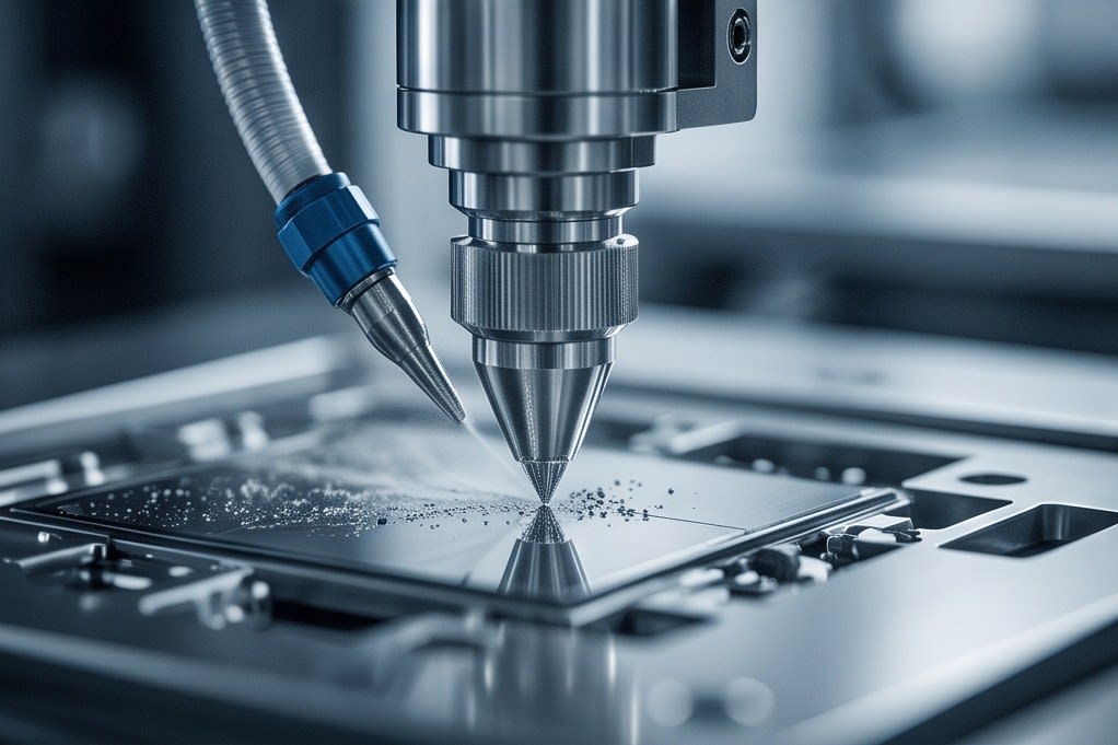
    Cleaning technology with an ultra-precision nozzle

    The Core of Semiconductor Processes, Precision Cleaning Technology

    The Impact of Micro Contamination on Yield

    In semiconductor manufacturing processes, the cleanliness of the wafer surface is a key indicator that determines the final product yield. In the modern semiconductor ecosystem, where nanoscale micro processes have become routine, even a tiny residue invisible to the eye can disrupt the pattern of fine circuits and become a critical variable that produces defective products in large quantities. Defects caused by this micro contamination directly lead to enormous cost losses for companies and ultimately weaken price competitiveness in the market.

    Huvics’ Technical Solution

    Huvics deeply understands these on-site concerns and provides the following technical solutions.

    • Solving challenging defect issues in semiconductor tape bonding processes
    • Overcoming technical difficulties encountered in tray cleaning processes
    • Responding based on extensive hands-on experience accumulated in the field

    We go beyond simply providing cleaning and support automation and simplification design across the entire manufacturing process of our customers. Through this, companies can significantly reduce unnecessary operating costs while maximizing consistency and stability in process quality. Precision cleaning technology ultimately lowers defect rates, optimizes equipment uptime, and improves overall productivity.

    With Huvics, which continues to build unmatched technological capabilities in precision cleaning and automation equipment through constant research and development, experience the highest production yield your semiconductor process can achieve.

    Site-Customized Process Redesign

    Solving Technical Challenges and Optimizing Processes

    The solutions provided by Huvics go beyond the step of simply removing contamination. They focus on fundamentally solving technical challenges in manufacturing sites and redesigning process workflows. In particular, Huvics presents site-customized response strategies by dramatically improving micro defect issues in the tape bonding process, a chronic problem in the semiconductor industry, and overcoming the physical limitations of tray cleaning technology. The many variables encountered in the field are difficult to solve with a fragmented approach.

    Sustainable Innovation and Automation Integration

    Based on years of accumulated field data, Huvics builds the most efficient precision cleaning process and tightly integrates it with automation systems. By introducing precise process automation and process simplification, we reduce the burden of chronic operating costs faced by companies while also practicing sustainable innovation that maximizes process quality stability.

    Our proven technological capabilities, developed through close collaboration with leading global companies, have become the most powerful core driver for increasing production yield in increasingly sophisticated micro process environments. When the invisible obstacles that hinder process efficiency are removed one by one through the professional perspective of Huvics, your manufacturing competitiveness will finally reach results with a higher level of perfection.
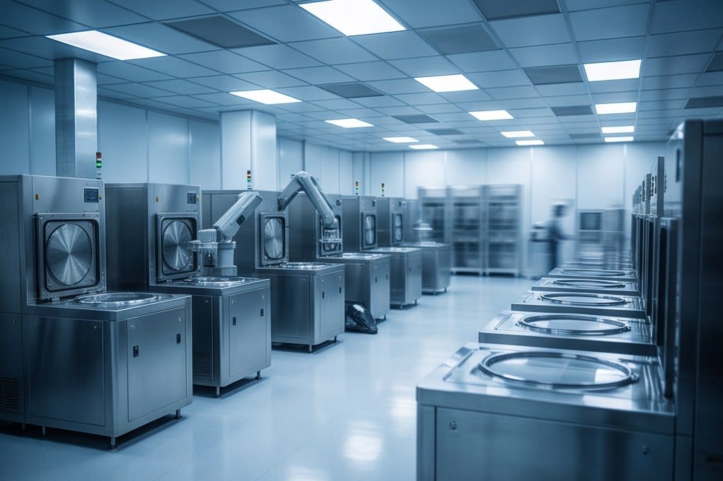
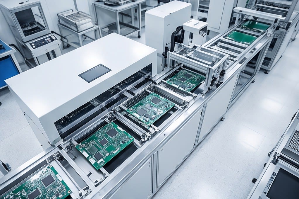
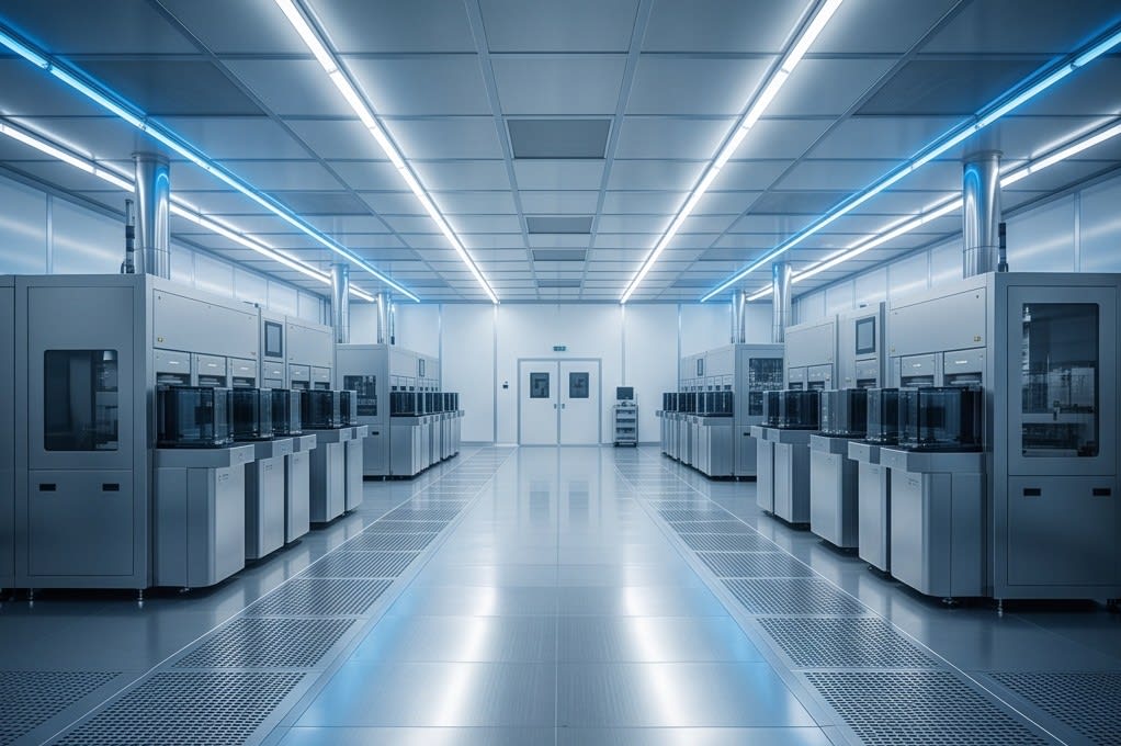
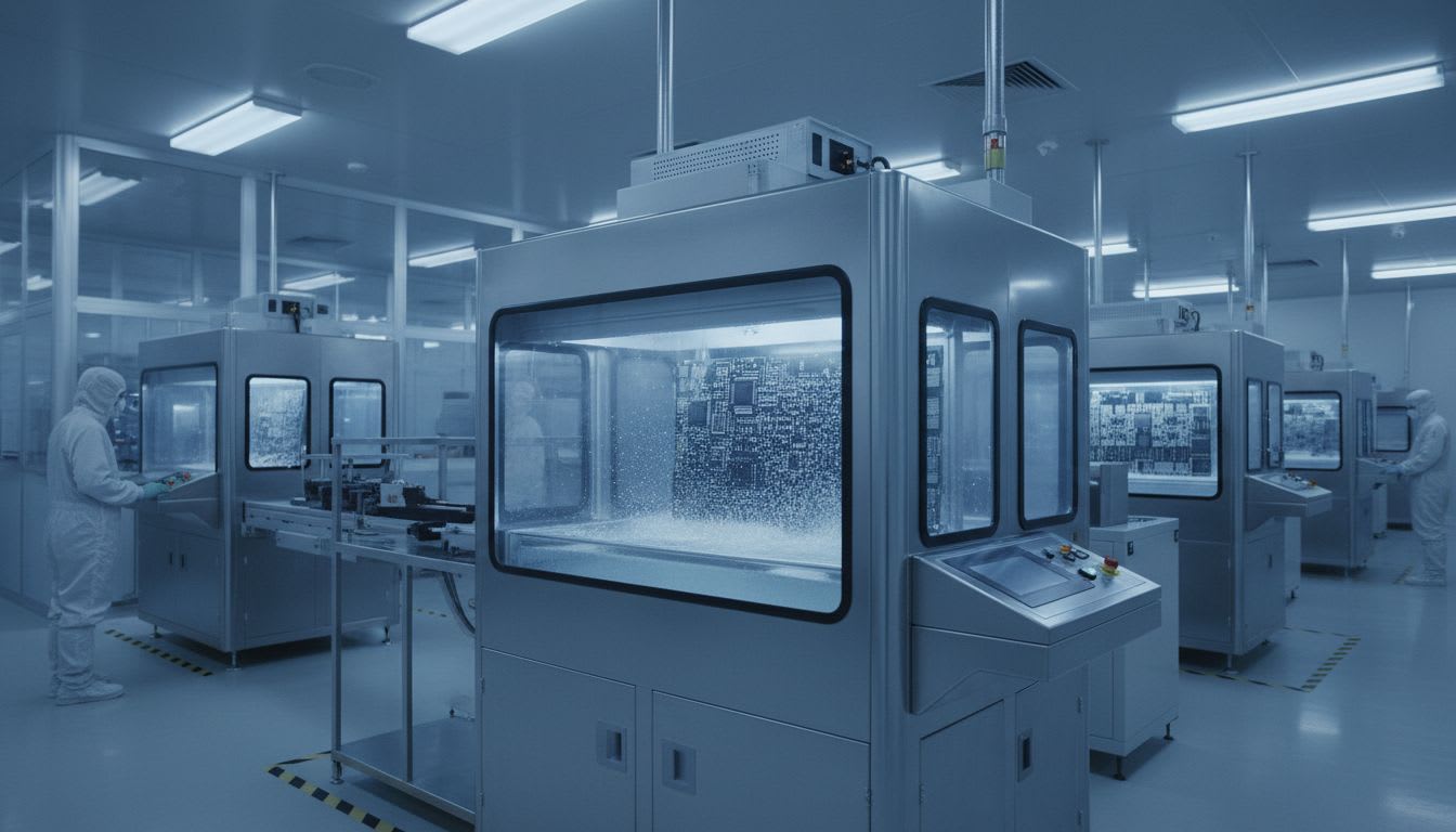
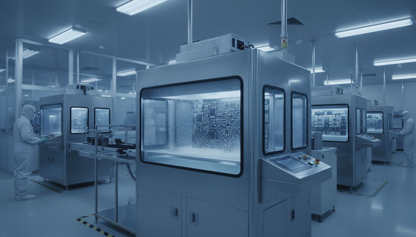
    Overview of automated equipment inside a cleanroom

    System-Based Automation Solutions

    Automation Systems for Quality Assurance

    Productivity in semiconductor manufacturing ultimately depends on how effectively invisible contamination is controlled. However, as processes become more complex, there are limits to direct human management. Huvics is advancing system-based automation solutions to address these limitations. Precision cleaning equipment is not simply a machine that wipes products clean. It is a quality assurance system that helps maintain consistent cleanliness from the beginning to the end of the process. Huvics technology, which blocks difficult contamination factors such as tape residue and fine particles at the source, is installed at key points across semiconductor production lines to continuously monitor potential threats.

    Improving Productivity and Preventing Human Error

    Reducing defect rates in the field is not simply about preventing losses. It is about increasing the mass production share of high-value-added products. Huvics diagnoses inefficient manual processes that customers struggle with and replaces them with the latest automation equipment, minimizing the room for human intervention. This improves the work environment, prevents human error, and dramatically enhances process efficiency. Huvics solutions, which integrate technical know-how accumulated in the field, solve the practical challenges customers face and help them secure manufacturing competitiveness at the next higher level.
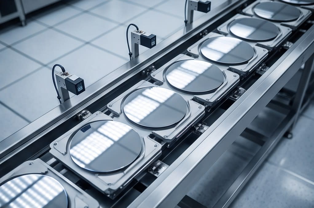
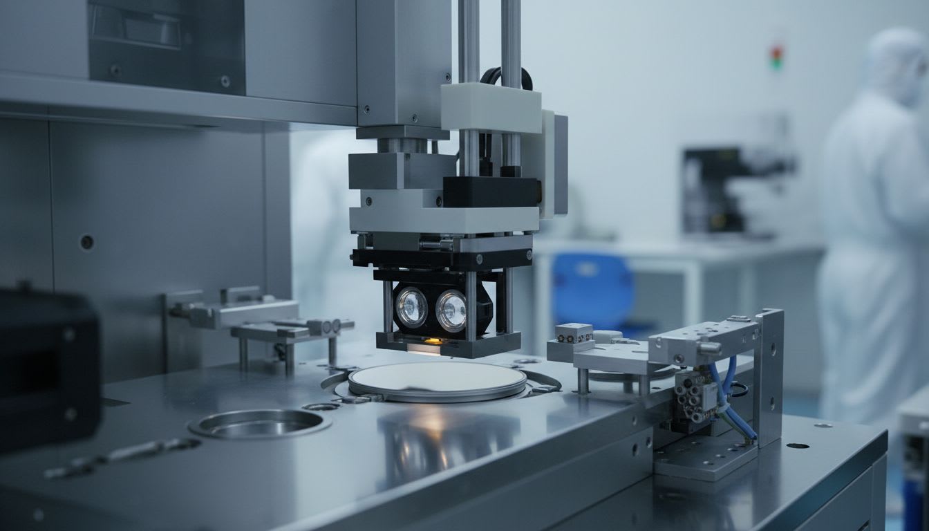
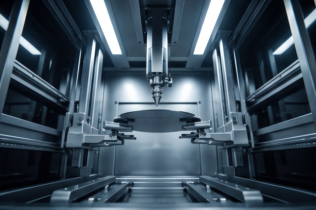
    Efficient wafer process flow

    Huvics Technology Portfolio and Future Value

    Business Success Through Customized System Implementation

    The broad technology portfolio held by Huvics is the most powerful tool for actively responding to the demanding requirements of the rapidly changing semiconductor market. Based in Osan, Gyeonggi-do, we continue to invest in research and development while advancing our technological capabilities in precision cleaning and automation equipment. On this foundation, we accurately diagnose inefficiencies in the complex manufacturing processes faced by customers and build customized systems that boldly reduce unnecessary steps, thereby substantially driving the business success of our partners. Maintaining stable quality standards amid a rapidly changing market environment is more important than anything else, and Huvics aims to be your trusted supporter at the center of creating those standards.

    Partnership for Process Innovation

    Beyond simply improving existing problems, an innovative approach that changes the paradigm of the process presents higher quality standards in the next generation semiconductor industry while also becoming a solid foundation for sustainable growth. Accumulated technological expertise in precision cleaning and deep understanding of field automation are the distinctive competitiveness of Huvics. We will provide full technical support so that your company can go beyond simple cleaning, enhance the perfection of the entire process, and achieve overwhelming production yield in the market. Through the precise technology and sincere partnership of Huvics, complete your process innovation and create future value together through higher production yield.
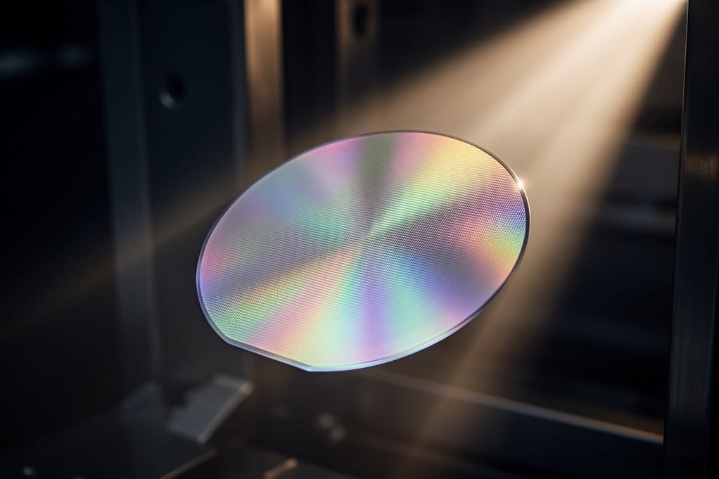
    Final quality of a defect-free wafer

    In semiconductor manufacturing, invisible micro contamination becomes a decisive variable that determines corporate competitiveness. Because cleanliness that may seem minor creates the major result known as yield, process perfection is now completed through collaboration with a partner that has technical insight.

    Based on precision cleaning technology and process automation solutions that fundamentally solve complex on-site challenges, Huvics will help your company surpass the limits of production yield and take the lead in the market. Removing invisible obstacles and innovating the process paradigm. Now, add overwhelming growth momentum to your business through the professional perspective of Huvics.


    Huvics is an advanced technology company that develops and manufactures automation equipment and
    production systems across the semiconductor, LED, Mobile, and Cosmetic industries.
    With top talent and continuous technological innovation, we support customers in improving productivity and
    securing quality competitiveness.

    Huvics Contact Information

    Phone: 031-374-8285
    Email: cdpark@huvics.com

    Contact Huvics

  • Huvics Micro Pattern Quality Innovation Strategy Powered by Ultrasonic Dispersion Technology and Intelligent Vision Inspection

    Huvics Micro Pattern Quality Innovation Strategy Powered by Ultrasonic Dispersion Technology and Intelligent Vision Inspection

    Huvics

    In increasingly complex smart devices, even a microscopic contaminant that cannot be seen with the naked eye can disrupt overall yield. This is a challenge that many people on the manufacturing floor have faced at least once. Foreign particles hidden between the micro patterns of highly integrated components are difficult to control completely with conventional cleaning methods alone, making the need for stable quality in production environments even more urgent.

    Huvics precisely identifies these on-site challenges and presents a new solution that combines proprietary ultrasonic dispersion technology with intelligent vision inspection. Let us explore an innovative strategy for minimizing defect rates and maintaining global-level quality even in demanding process environments.

    View of a smart factory

    Key Challenges in Highly Integrated Component Manufacturing and Huvics Ultrasonic Technology

    Microscopic Contaminants and Process Limitations

    In advanced electronic component manufacturing sites, especially in processes that produce highly integrated components such as multilayer ceramic capacitors or flexible circuit boards, microscopic contaminants are more than simple dust to be removed. They are decisive variables directly linked to product performance, because even a single fine particle can determine overall yield.

    The reality is that contamination in these micro patterns encountered on the manufacturing floor is difficult to resolve fundamentally with conventional cleaning methods. To overcome these limitations, Huvics has introduced proprietary ultrasonic dispersion technology into the process and adopted an advanced approach that precisely controls the process environment itself.

    Technical Features of Ultrasonic Dispersion Technology

    The technical features of Huvics are as follows.

    • Uniformly disperses material particles inside liquid at the micro level to prevent quality variation
    • Maximizes cleaning efficiency by optimizing the physical properties of the material itself beyond removing external foreign substances
    • Provides precision control that completely removes even the smallest contaminants remaining between micro patterns

    This precision control capability has become a core driving force that dramatically improves production efficiency on the manufacturing floor, establishing a new standard for high-value-added component manufacturing.

    Precision cleaning of micro pattern circuits

    Completing Quality Control Through Intelligent Systems

    Integration of the Inspection Process After Cleaning

    The technical value provided by Huvics does not stop at the cleaning process that simply washes away contamination. Building an intelligent system that considers the stages after cleaning becomes an important foundation for raising the completeness of quality control to the next level.

    After precisely cleaning micro patterns with its proprietary ultrasonic dispersion technology, Huvics intelligently integrates advanced vision inspection algorithms into the inspection process that immediately follows. This is a sophisticated design intended to instantly identify even the smallest defects in highly integrated components in real time and maximize reliability from the initial assembly stage.

    Solutions for Global Competitiveness

    In a market environment where smart device specifications continue to rise and internal designs become more complex, the biggest concern for manufacturers is how to minimize defect rates and maintain consistent quality even in demanding process environments. The solution from Huvics provides the clearest answer to this challenge.

    • Fully controls process variables through precision cleaning using ultrasound
    • Responds proactively to market changes through real-time monitoring using vision algorithms
    • Supports customers in securing a distinctive technological advantage in global competition

    Automated PCB inspection process

    The Value of Huvics That Defines Manufacturing Competitiveness

    Controlling contamination in micro patterns goes beyond a simple cleaning issue. It is a critical strategic asset that determines the yield of high-value-added products. The approach of Huvics, which blocks fundamental quality variation with ultrasonic dispersion technology and protects process reliability to the end with intelligent vision inspection, is now becoming a clear standard for determining manufacturing competitiveness in the rapidly changing smart device market.

    Remember that an invisible and very small difference ultimately creates a major gap that leads the entire market. Huvics will stand with you as the most reliable and professional partner on the innovative journey toward the perfect production environment your company pursues.


    Huvics is an advanced technology company that develops and manufactures automation equipment and
    production systems across the semiconductor, LED, mobile, and cosmetics industries.
    With top-tier talent and continuous technological innovation, we support customers in improving productivity and
    securing quality competitiveness.

    Huvics Contact

    Phone: 031-374-8285
    Email: cdpark@huvics.com
    Contact Huvics

  • Key Technologies of the Huvics One-Stop Integrated System That Maximizes Semiconductor Cleanroom Process Efficiency

    Key Technologies of the Huvics One-Stop Integrated System That Maximizes Semiconductor Cleanroom Process Efficiency

    Huvics

    Leaders in the semiconductor industry say with one voice that reducing even the smallest process deviations is the path to pushing beyond the limits of yield. In a cleanroom environment where not even a single invisible particle of dust can be tolerated, physical transfer between processes itself carries critical contamination risks and inefficiencies.

    To solve these challenges, Huvics has achieved innovation by integrating the core stages of lamination, tape mounting, and UV curing into one system. Moving beyond simple equipment adoption, let us look at why the one-stop technology from Huvics, which is fundamentally reshaping production structures on manufacturing sites, has become the most powerful strategic choice for semiconductor manufacturers.

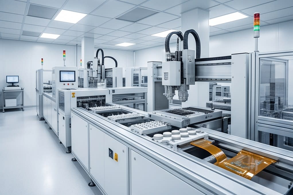
    Inside the Huvics integrated system

    Innovation in Semiconductor Processes, the Huvics One-Stop System

    Cleanroom Environment and Process Optimization

    A cleanroom at a semiconductor manufacturing site is a space that requires an extreme level of cleanliness where even a tiny particle of dust cannot be allowed. Because it is a sensitive environment where just one small particle can determine overall yield, manufacturers face the challenge of securing a higher level of precision and process stability than ever before.

    Key Features of the Integrated Process

    To satisfy these strict standards, Huvics has introduced a one-stop system that integrates three core processes, lamination, tape mounting, and UV curing, into a single piece of equipment. The main features of the system provided by Huvics are as follows.

    • Eliminates physical transfer to block contamination risks at the source
    • Implements a design that optimizes occupied space inside the cleanroom
    • Enhances operational completeness and presents a standard for manufacturing efficiency

    Ultra precision nozzle operation

    Precision Control Technology and Maximized Production Efficiency

    LED-Based UV Curing Technology

    The technological differentiation of the Huvics system is concentrated in its precisely designed LED-based UV curing technology. In semiconductor assembly processes, bonding quality is a critical factor that determines the reliability of the final product, and the Huvics system delicately controls consistent light intensity and wavelength to maintain bonding strength at the most ideal level.

    Reduced Defect Rate and Shortened Tact Time

    This precision control capability secures the reliability of subsequent processes while dramatically lowering the defect rate. The tact time required in complex assembly lines is shortened through this efficient curing process, becoming a powerful tool for meeting the extremely demanding quality standards required by manufacturers.

    Based on the belief that technology is process optimization itself, and that this optimization directly leads to manufacturer competitiveness, Huvics continues to evolve to maximize production efficiency.

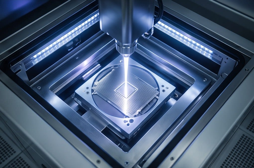
    Precise UV curing process

    Improving Cost Structure and Securing Future Competitiveness

    Integrated Solution for Improving Production Efficiency

    Simplifying processes goes beyond shortening work time and becomes the key to fundamentally improving a manufacturer’s cost structure. By reducing the operational burden created by running multiple pieces of equipment separately and handling all core stages with a single one-stop system, production efficiency improves dramatically.

    Huvics as a Strategic Choice

    This integrated solution is a strategic option that enables companies to solve the challenges of cost reduction and productivity improvement in semiconductor production sites all at once. Through innovative efforts to raise process efficiency to the highest level, Huvics is building an even stronger structure for semiconductor production lines.

    The technological capabilities of Huvics, which are defining new process standards for global semiconductor cleanrooms, are establishing themselves as a reliable investment and strategic choice for manufacturers seeking to secure future competitiveness.

    Huvics cleanroom view

    Closing Remarks

    As discussed above, the completeness of technology depends on how efficiently it compresses processes and eliminates uncertainty. The challenges of contamination risk and process delays faced by semiconductor manufacturing sites have been transformed into opportunities for optimization through the integrated solution from Huvics.

    As the need to maximize production efficiency while improving cost structures becomes more important, the innovative process standard presented by Huvics will become the most reliable answer. We invite you to experience firsthand how the power of technology that precisely controls even the smallest invisible details will change the future of semiconductor manufacturing.

    Completed semiconductor wafer


    Huvics is an advanced technology company that develops and manufactures automation equipment and
    production systems across the semiconductor, LED, Mobile, and Cosmetic industries.
    With top talent and continuous technological innovation, we support customer productivity improvement and
    quality competitiveness.

    Huvics Contact Information

    Phone: 031-374-8285
    Email: cdpark@huvics.com
    Contact Huvics

  • How to Improve Semiconductor Packaging Process Efficiency and Quality Stability with the Huvics Laminator System

    How to Improve Semiconductor Packaging Process Efficiency and Quality Stability with the Huvics Laminator System

    Huvics

    As semiconductor packaging technology advances rapidly and demands even higher precision, overcoming process limitations has become not a choice but a matter of survival. In particular, inefficient waiting time and physical movement caused by segmented steps from cleaning to assembly remain unresolved challenges for site managers who must increase productivity.

    Is it possible to create an ideal process environment that integrates complex steps while maintaining quality reliability? The one-stop laminator system proposed by Huvics is the answer to this challenge, fundamentally changing the paradigm of manufacturing sites by organically integrating process flow.

    Robotic arm improving efficiency through automation

    A One-Stop System That Improves Semiconductor Process Efficiency

    Stacked Packaging and Process Challenges

    The modern semiconductor industry requires a higher level of precision than ever before. In particular, as stacked packaging technology advances dramatically, the accuracy of the process that stably builds numerous layers has become a key competitive advantage that determines a company’s market share.

    In this environment, semiconductor assembly sites face even more demanding challenges. Conventional cleaning and assembly processes are separated by each step, causing repeated physical movement and waiting time, which inevitably leads to inefficient takt time and hinders productivity improvement.

    Huvics Integrated Laminator Innovation

    Huvics provides the answer at this exact point. Beyond simply advancing individual equipment, its one-stop laminator combines tape mounting and UV curing technology into one original system.

    From expansion to the final stage of UV curing, Huvics innovation processes every step continuously within a single piece of equipment, overcoming existing physical limitations at once and opening a new paradigm in process efficiency.

    Precisely seated wafer process

    Quality Stabilization Through Precision UV Curing Technology

    Adhesion Strength Control and Defect Prevention

    The reason the Huvics one-stop laminator system receives outstanding evaluations in the field is not only that it physically integrates the process flow. Behind it lies the technological essence of a precision UV curing mechanism that strategically combines lamps and LEDs.

    Controlling the adhesion strength of tape during the semiconductor packaging process is a highly sensitive task that determines the stability of the final product. If adhesion is too strong, it can damage devices during removal, and if it is too weak, it can cause defects such as misalignment during the process.

    Implementation of precision UV curing technology

    Improved Reliability of the Production Line

    The Huvics system finely controls this adhesion strength to maintain the optimal condition. This precise control technology functions as a safeguard that blocks potential defect factors that may occur during production at the source.

    As a result, site managers can reduce anxiety about defect rates and operate production lines in a much more stable environment. This is not simply a replacement of equipment, but a strategic investment that fundamentally raises the reliability of manufacturing quality to a higher standard.

    Huvics

    Securing Market Competitiveness Through Technological Completeness

    Consistent Process Results and Efficiency

    At semiconductor manufacturing sites, quality reliability is directly connected to customer trust. Huvics technology systematically ensures the completeness of the entire process, from the cleaning process to subsequent assembly stages.

    Unlike past methods that required countless trials and errors to meet demanding process conditions, the integrated system from Huvics delivers consistent results. In particular, the LED-based UV curing environment maximizes energy efficiency while ensuring uniform curing performance, raising product reliability to the highest level.

    A Production Line Optimization Partner

    For companies, this kind of technological stability becomes the strongest foundation for securing unwavering competitiveness in the market. Maintaining high yields without defects while responding flexibly to the rapidly changing demands of the semiconductor market, Huvics realizes this ideal manufacturing site and establishes itself as a powerful partner that optimizes production line operations beyond the role of a simple supplier.

    Production site of a smart factory

    Integrated Solutions for Future Manufacturing Sites

    An Engine for Maximizing Productivity

    In conclusion, the one-stop laminator system from Huvics is the optimal engine for solving the long-standing corporate goal of maximizing productivity. It dramatically reduces waiting time between process stages and minimizes the possibility of human error through automated precision control, maximizing on-site efficiency.

    This goes beyond simply reducing costs and organically improves the flow of the entire process, enabling resilient responsiveness to future changes in the technology environment. In an environment where stacked packaging technology continues to advance, this kind of technological choice that secures both process efficiency and quality stability is essential.

    Advanced semiconductor manufacturing cleanroom

    Enhancing Business Value

    This integrated solution proposed by Huvics clearly shows the direction semiconductor manufacturing sites should take. If your company seeks to build a defect-free production system based on high technological completeness, elevate your business to the next level through the innovative process integration engine from Huvics.

    As semiconductor processes become more complex, the flexibility and precision to connect segmented stages into one have become key values that determine corporate survival beyond simple competitiveness. The one-stop laminator system from Huvics breaks down the walls of inefficiency that hinder production flow and presents a technological milestone that raises the completeness of the entire process to the next level.

    At today’s manufacturing sites that demand advanced precision, design the future of your process through a proven integrated solution instead of worrying about unnecessary waiting and defects. The unwavering stability realized by Huvics will bring optimal efficiency and trust to your production line.


    Huvics is an advanced technology company that develops and manufactures automation equipment and
    production systems across the semiconductor, LED, Mobile, and Cosmetic industries.
    With outstanding talent and continuous technological innovation, we support customer productivity improvement and
    quality competitiveness.

    Huvics Contact

    Phone: 031-374-8285
    Email: cdpark@huvics.com
    Huvics Inquiry