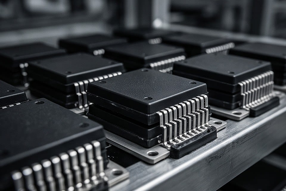

If defects are found in parts after cleaning, the loss has already started somewhere in the process. Thickness variation in the grinding stage, uneven adhesion in the tape attachment process, contamination residue remaining after cleaning — if even one of these three issues is overlooked, yield loss and rework costs can grow rapidly. The later a problem appears in the downstream process, the more correction costs increase exponentially, and delayed delivery can even undermine customer trust.

Thickness Uniformity in the Grinding Process Determines Yield
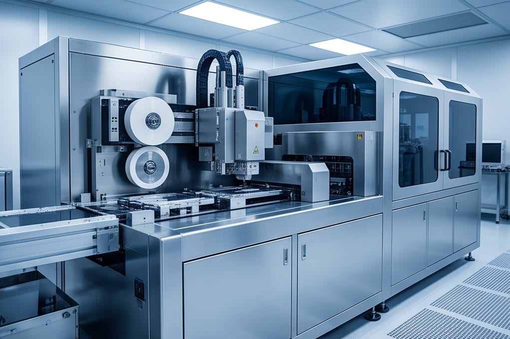
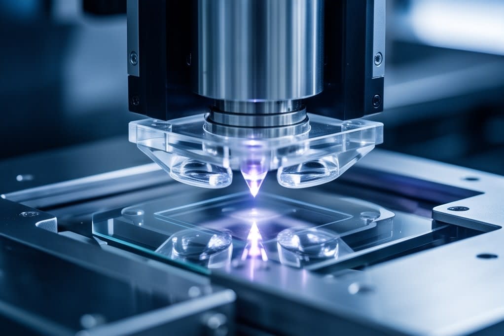
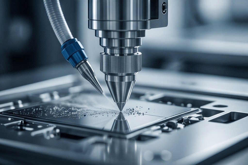
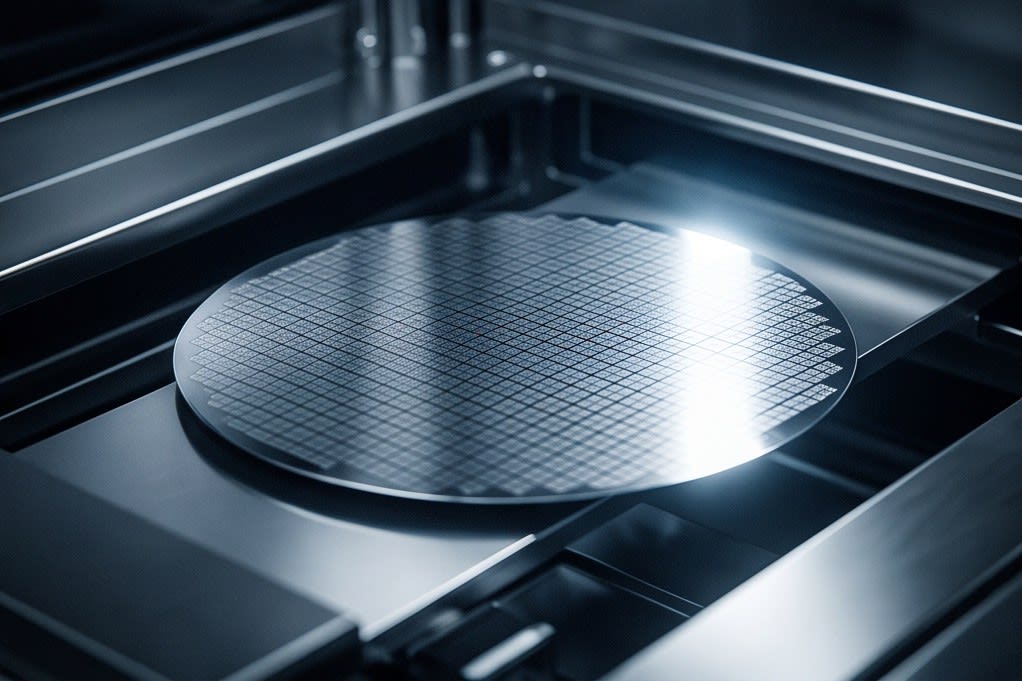
In the semiconductor packaging process, thickness uniformity is one of the most sensitive variables that determines yield. Modern package structures such as WLCSP wafer level chip scale package, FCBGA, and QFN are based on vertical chip stacking, and if the thickness after grinding is even slightly uneven, stacking chips on top becomes impossible.
According to analysis by AE Research, the thickness uniformity tolerance required in semiconductor grinding processes is less than 1 micron, and chips outside this standard immediately lead to defects in the stacking process. This is why micron level precision grinding using diamond wheels is not simply a machining technology, but a prerequisite for package reliability. To maintain this level of tolerance consistently even in high speed processes, stage precision and consistent grinding conditions must both be secured. Keeping thickness variation within the allowable range is the key to high yield production.

Integrated Lamination Processes Prevent Error Accumulation
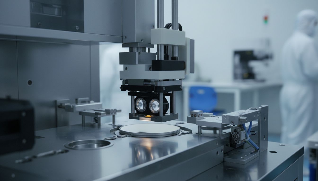
The more a process is divided into multiple stages, the more errors accumulate between each stage. When tape attachment, UV curing, and expanding are performed on separate equipment, alignment can shift or adhesion conditions can vary during transfer between processes.
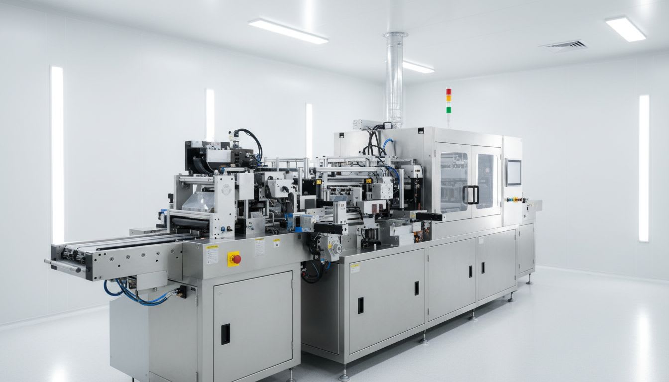
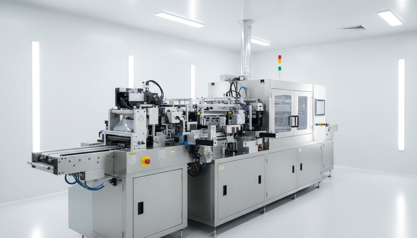
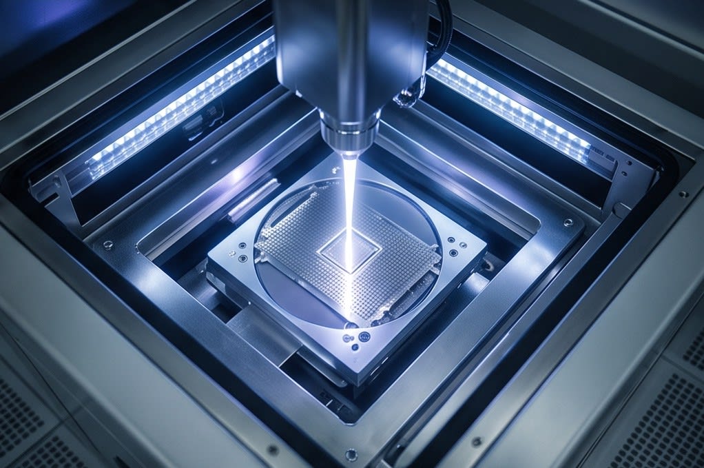
The laminator system from Huvics structurally prevents this issue by integrating key processes from the expander to UV curing within a single system. In the UV curing stage, uniform irradiation intensity is especially important. Uneven UV irradiation causes film shrinkage and adhesion variation, increasing the risk of damage in the subsequent chip separation process. In contrast, when UV curing is performed under controlled conditions, tape adhesion weakens predictably, allowing chips to be separated without damage.
A UV curing system that can selectively apply lamp and LED methods provides the flexibility to respond according to product type and production volume. Connecting processes into one continuous flow and reducing the number of transfers is itself implemented as a way to secure both shorter takt time and process stability.

The Cleaning Process Is the Final Gateway to Quality
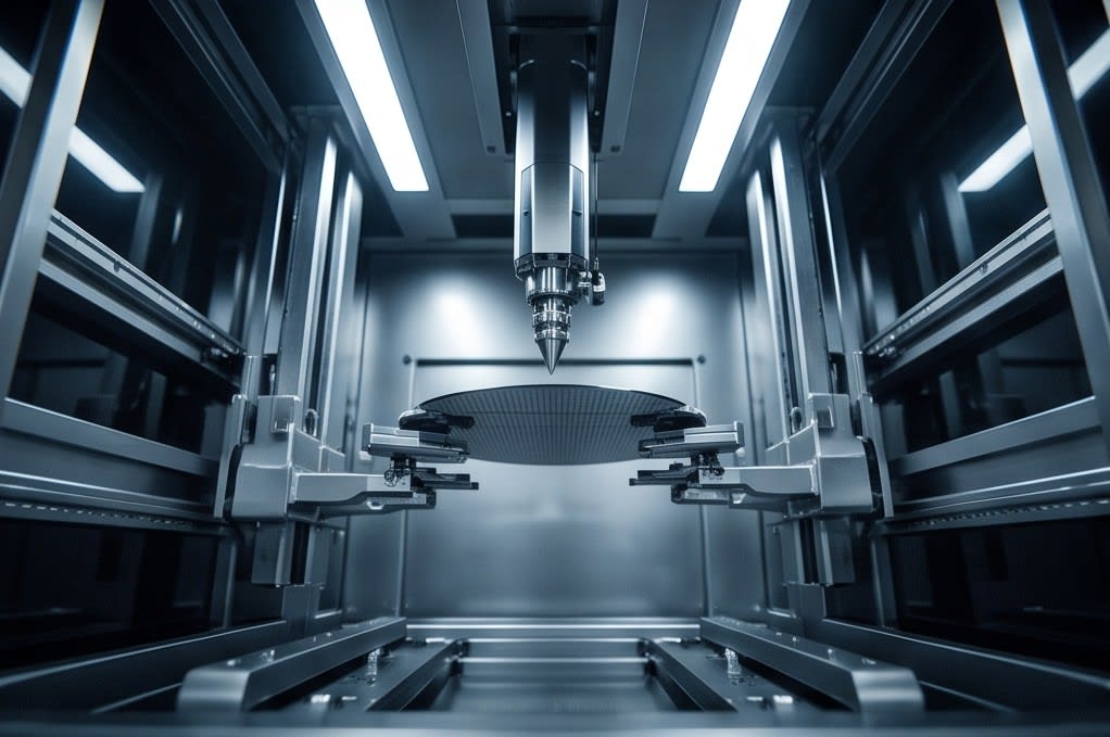
No matter how precise the machining and attachment processes are, final quality becomes unstable if contaminants remaining on the surface are not removed. In camera module manufacturing sites, if residual flux and contamination particles generated during the reflow process after CSP assembly are not removed through cleaning, ionic residues cause corrosion and directly affect module performance.
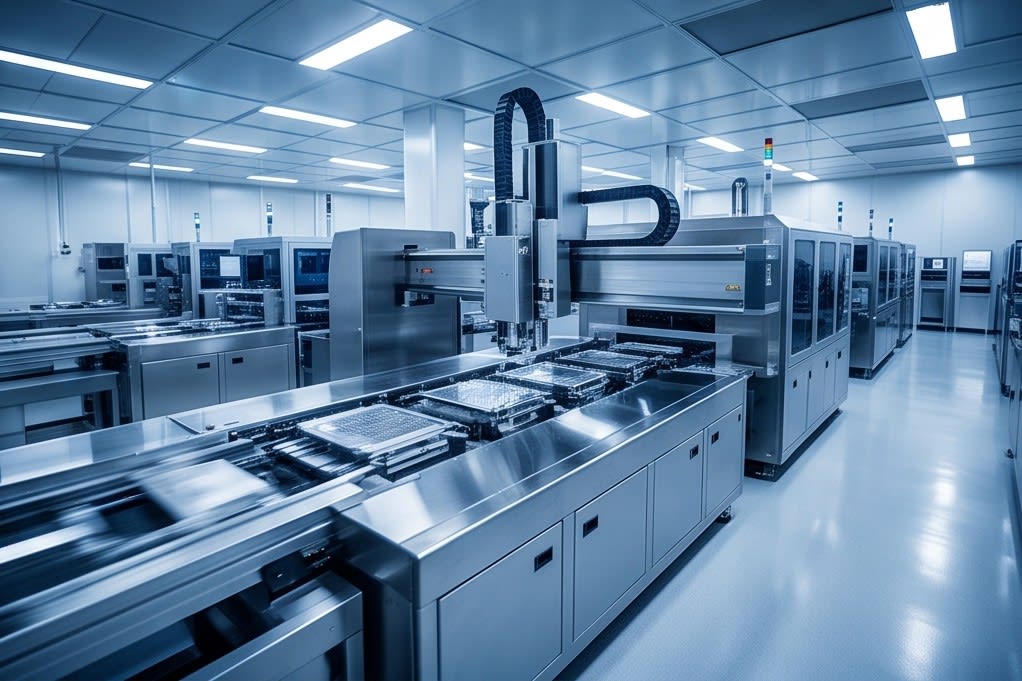
In production environments that handle components with diverse shapes and materials, such as VCM motors, image sensors, and trays, a single cleaning method makes it difficult to respond to all types of contamination. The cleaner system from Huvics removes surface contamination particles step by step through a multi stage cleaning method that combines micro bubbles, water jet, and air knife, and it also includes an oven drying function to remove residual moisture after cleaning.
Full auto and manual methods can be selected, allowing flexible application depending on the line configuration. In automated configurations, worker intervention between processes is minimized, reducing the risk of contamination reattachment. In the field, results show that as the defect rate in the cleaning stage decreases, the downstream rework rate also drops.

Micron level precision in the grinding process, an integrated flow in the lamination process, and multi stage contamination removal in the cleaning process — these three elements are not separate technologies, but one connected line of defense against semiconductor defects. Weakness in any one stage is transferred as a burden to the next stage, and the structure in which it is ultimately confirmed as a defect in final inspection will inevitably repeat unless the entire process is designed with precision. Controlling variation at each point in the process is a far more cost effective way to protect quality than tracing the cause after a defect occurs.
Huvics is an advanced technology company that develops and manufactures automation equipment and
production systems across the semiconductor, LED, Mobile, and Cosmetic industries.
With top talent and continuous technological innovation, we support customer productivity improvement and
quality competitiveness.
Huvics Contact
Phone: 031-374-8285
Email: cdpark@huvics.com