Tag: SemiconductorEquipment

  • Why Flatness Control Matters in Chip Stacking Processes and the Role of Grinding

    Why Flatness Control Matters in Chip Stacking Processes and the Role of Grinding

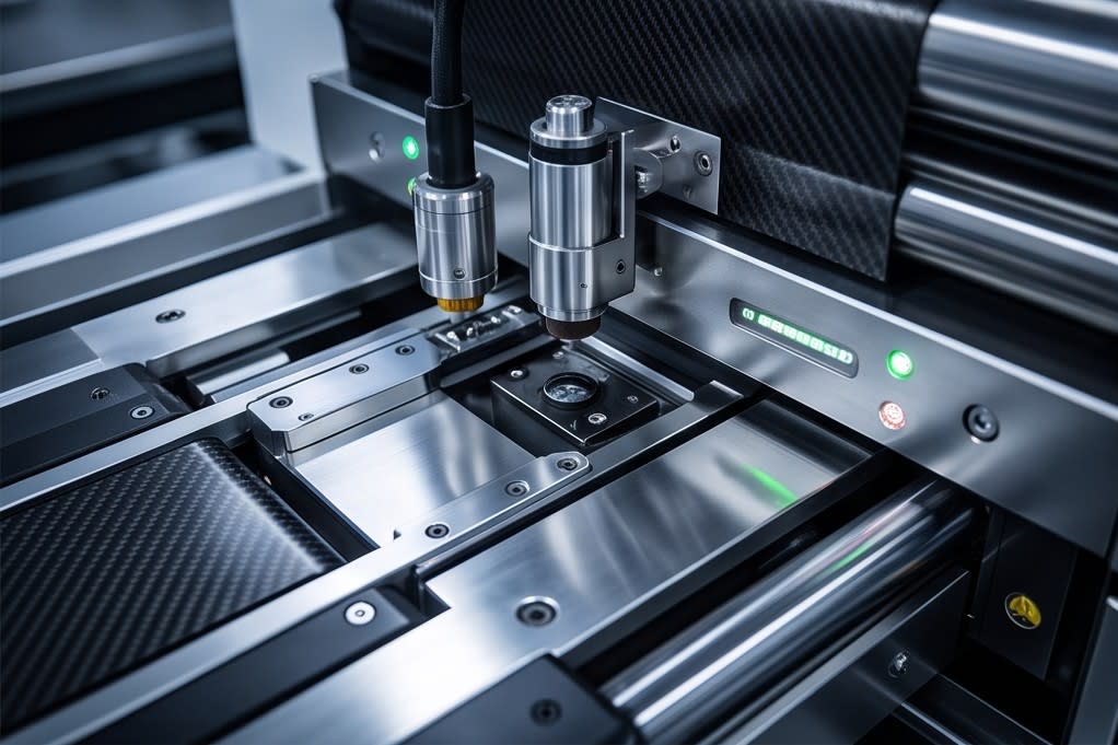
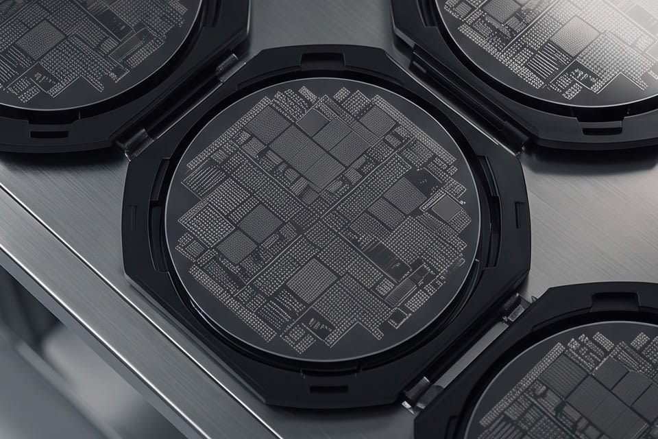
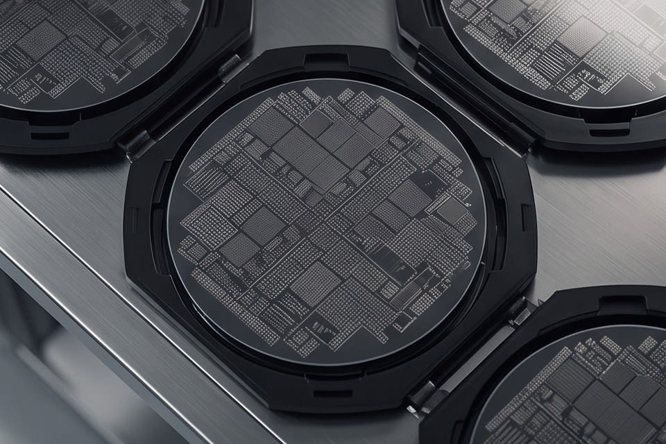
    Fine integrated structure of a semiconductor wafer seated on a fixture

    According to an analysis by Yole Group, a semiconductor packaging market research firm, the advanced packaging market is expected to grow by more than 10% annually through 2027, with the share of products adopting chip stacking structures expanding rapidly. As stacking chips in multiple layers becomes a core method for achieving higher performance, thickness uniformity and surface flatness between each layer are emerging as the most sensitive variables determining product reliability. What this figure shows is not simply market growth. It reflects the reality that as stacking structures become more complex, the process costs and yield losses caused by failed flatness control increase as well.

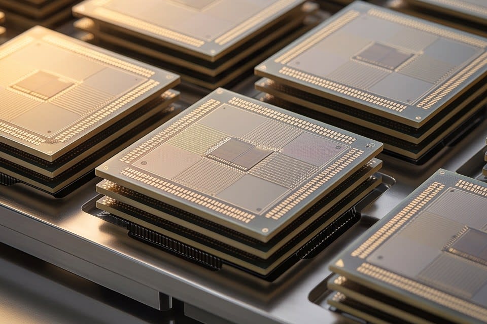
    High performance semiconductor chip structure precisely stacked vertically in layers

    Why flatness is critical in the chip stacking process

    In the process of stacking chips layer by layer, flatness is not merely an external appearance standard. Flatness, as defined by SEMI M1, an international semiconductor standards organization, numerically represents how much a wafer surface deviates from an ideal reference plane. In processes below 10 nanometers, total thickness variation (TTV, Total Thickness Variation) must be maintained below 1 micrometer, and the moment this standard is exceeded, the entire subsequent bonding process becomes unstable.

    The issue lies in the stacking structure itself. Thickness variation in the temporary bonding layer between chips determines the lower limit of grinding uniformity, and the nonuniformity that occurs in that layer is directly transferred to the next process step. A deviation created in just one layer can expand into alignment error across the entire stacked structure. This becomes even more pronounced in products such as AI semiconductors and high performance memory, where dozens of chips must be stacked. As the number of stacked layers increases, the speed at which initial flatness deviations accumulate also accelerates.

    In production sites, flatness defects usually become an issue after the grinding process, when subsequent processes are already underway. This creates a structure in which losses increase the later defects are detected.
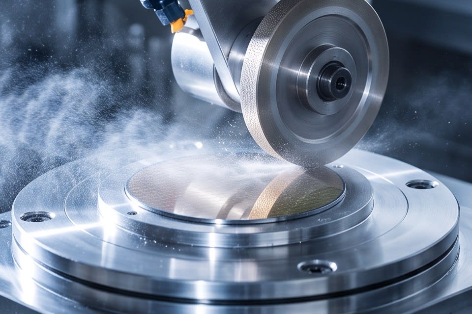
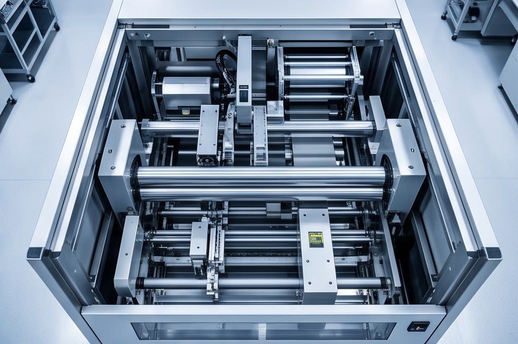
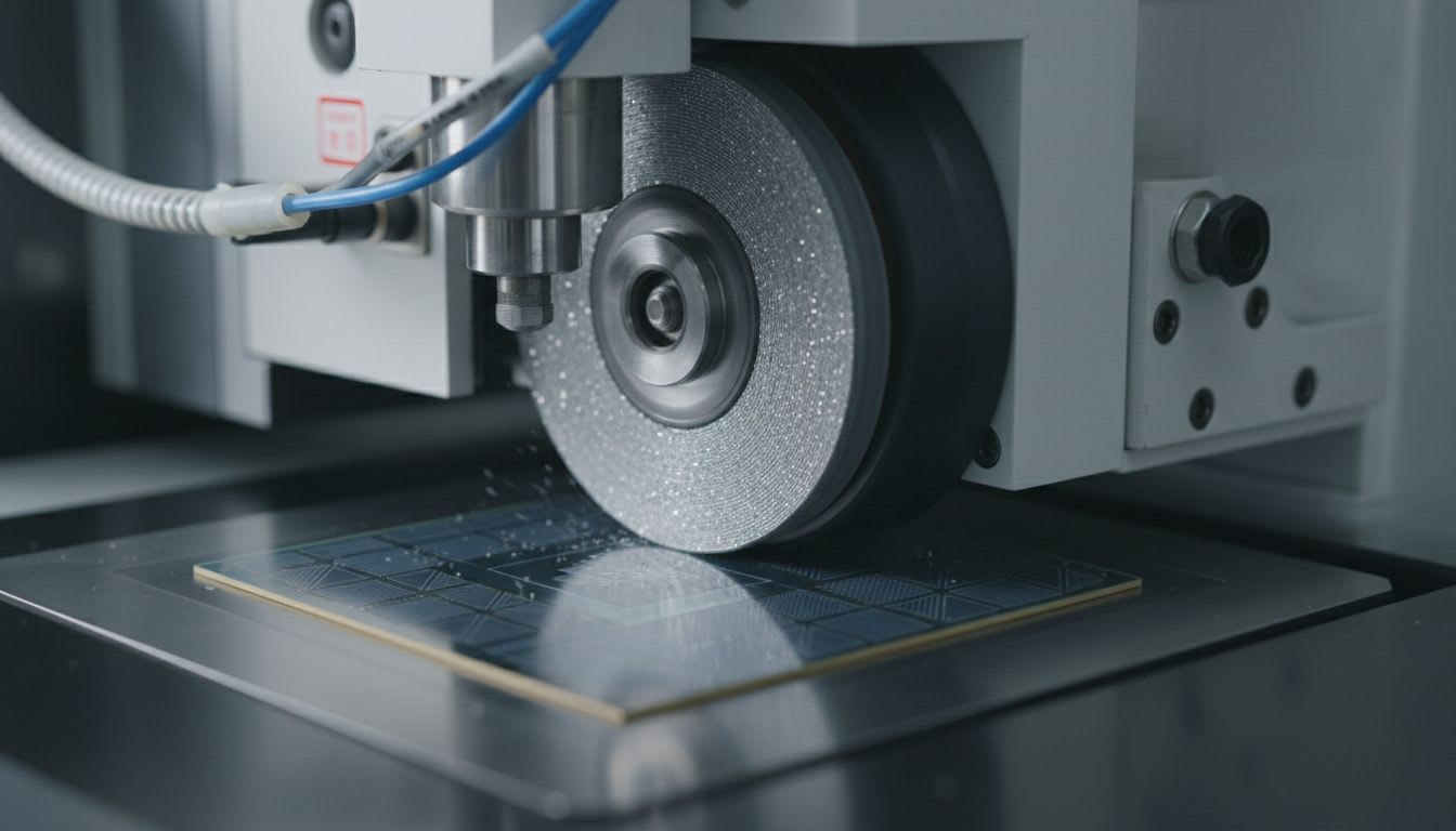
    Diamond wheel grinding process that uniformly processes the surface of a semiconductor wafer

    Technical design of the PKG Grinder and its response to flatness requirements

    The PKG Grinder addresses this issue at the equipment design level. To secure flatness in the grinding process, two conditions must be satisfied at the same time.

    • The precision of the stage that holds the package firmly so it does not move during processing
    • The cutting precision of the diamond wheel that uniformly removes the surface

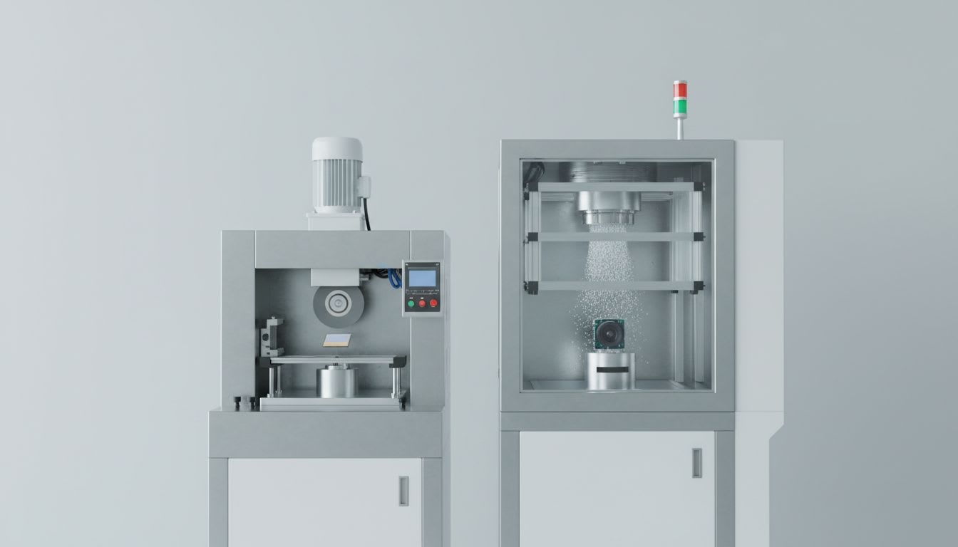
    The PKG Grinder combines a high precision stage with a diamond wheel to achieve micron-level thickness control. Whether the package type is FCBGA, WLCSP, QFN·DFN, or solar cell, the core role of this equipment is to process it uniformly to the target thickness required by the customer. No matter what package is handled, the standard is the same. It must be ground without deviation until the target thickness is reached.

    Depending on the production line configuration, users can choose from Full Auto (Type A·Type B) and Manual Type, enabling line design that considers both the level of automation and process flexibility. The design direction of this equipment is to improve yield by stably maintaining processing quality even under high speed process conditions. Ultimately, flatness control depends on how consistently and precisely grinding equipment handles the surface with controlled force and accurate motion paths.
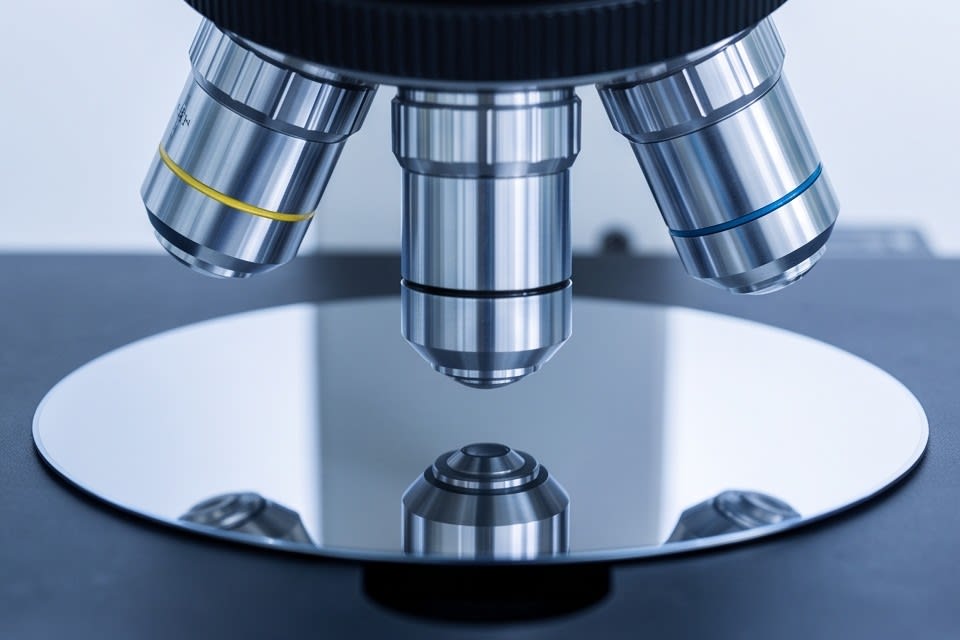
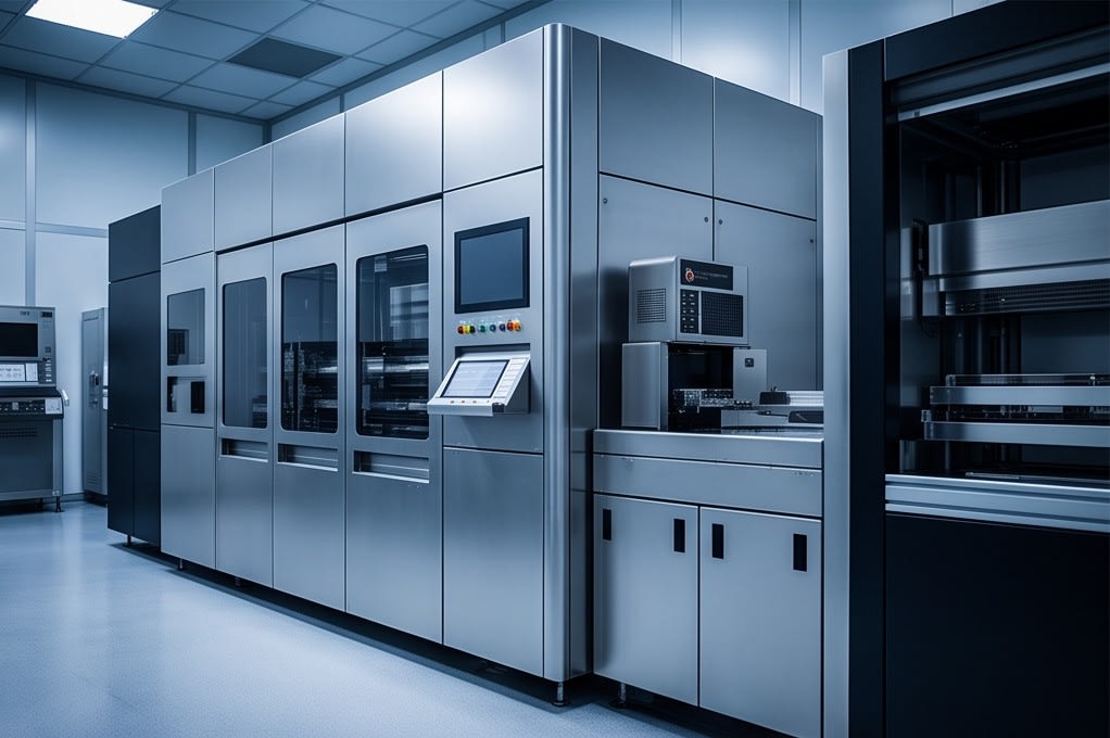
    Precision inspection that checks wafer surface condition using a laser after the grinding process

    Quality control extending to post grinding processes

    Flatness control is not complete simply because grinding has ended. After grinding, the surface condition must be inspected precisely, and the detection limit of modern inspection systems using laser scattering is approximately 20 to 30 nanometers. However, actual sensitivity varies greatly depending on the wafer surface condition. If residual contamination or fine scratches remain on the surface after grinding, the inspection accuracy itself may decline.

    There are also requirements that the contact surface roughness of packaging substrates must be controlled below 20 nanometers, and further below 5 nanometers, to form fine wiring. To reliably secure this level of surface quality, the precision of the cleaning process after grinding is also important. If the connection between grinding and cleaning is broken, it becomes difficult to guarantee precision at the inspection stage.

    As demand for AI semiconductors and high performance memory increases, the number of stacked layers and package complexity continue to rise. In a trend where required flatness standards and surface quality standards are becoming stricter at the same time, an integrated approach that covers the entire process is becoming increasingly important, beyond the performance of grinding equipment alone.
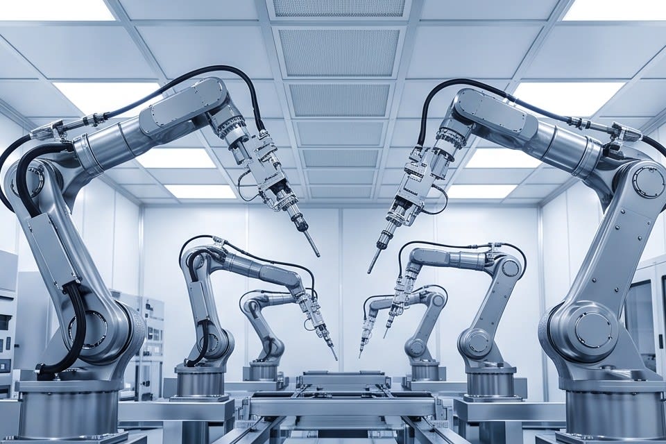
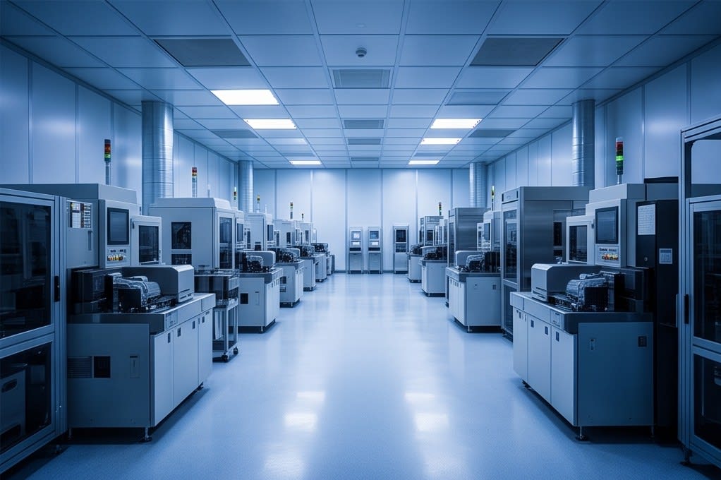
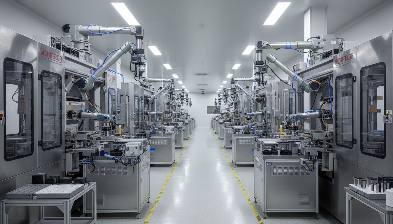
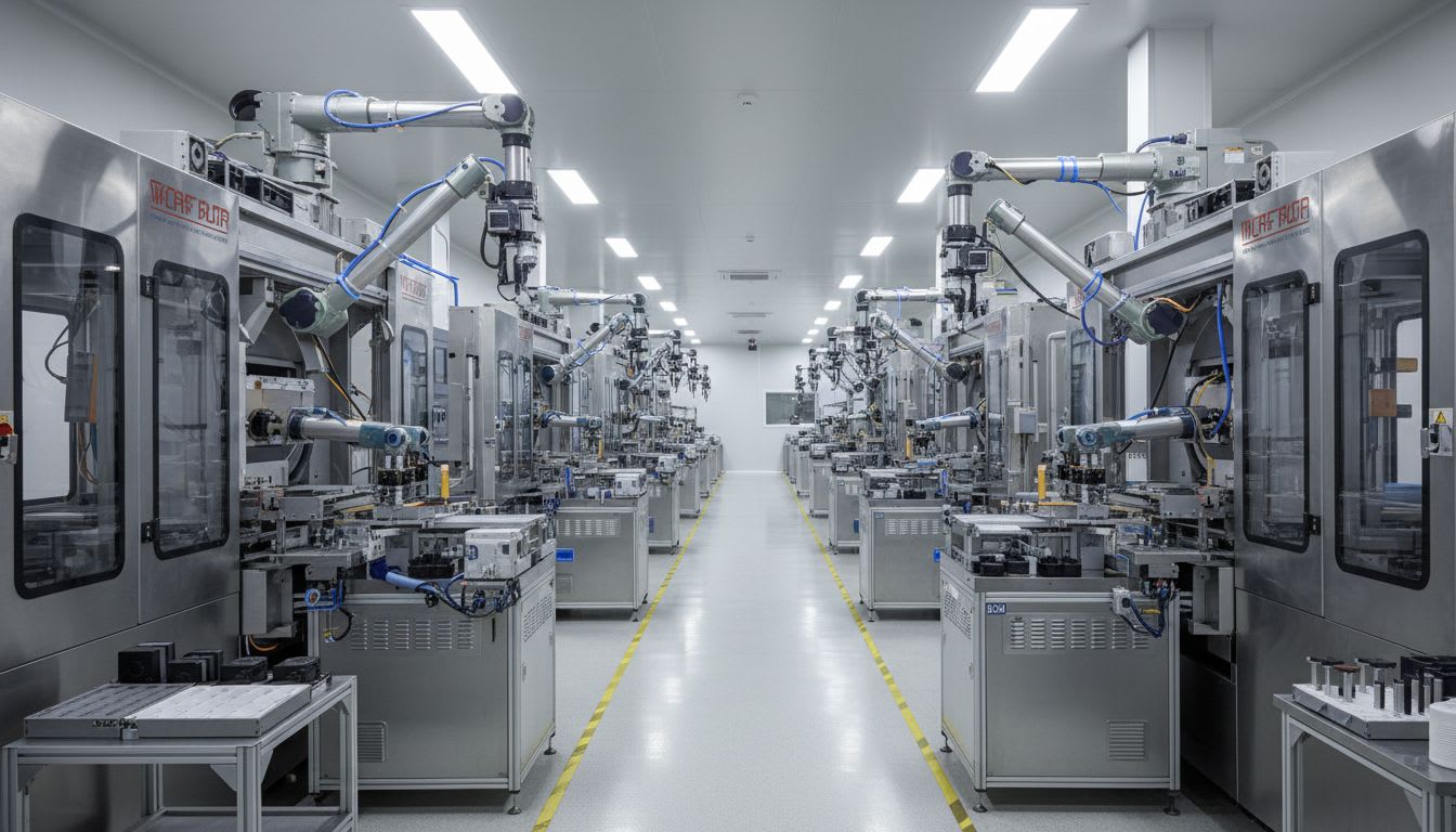
    Automated semiconductor production line that enables precise quality control and process efficiency

    The growth figure for the advanced packaging market mentioned in the first sentence ultimately leads to one question. In a situation where more chips must be stacked more thinly, how can flatness be maintained consistently. Only when the entire process, starting with the precision of grinding equipment and continuing through cleaning and inspection, is aligned to a single standard can the reliability of stacked structures be secured. In the chip stacking process, flatness control is not an issue of a single piece of equipment, but an issue of overall process design.


    Huvics is an advanced technology company that develops and manufactures automation equipment and
    production systems across the semiconductor, LED, Mobile, and Cosmetic industries.
    With outstanding talent and continuous technological innovation, we support customers in improving productivity and
    securing quality competitiveness.

    Huvics Contact

    Phone: 031-374-8285
    Email: cdpark@huvics.com

    Huvics Inquiry

  • Precision Grinding and Multistage Cleaning Core Principles That Determine Stacked Packaging Reliability

    Precision Grinding and Multistage Cleaning Core Principles That Determine Stacked Packaging Reliability

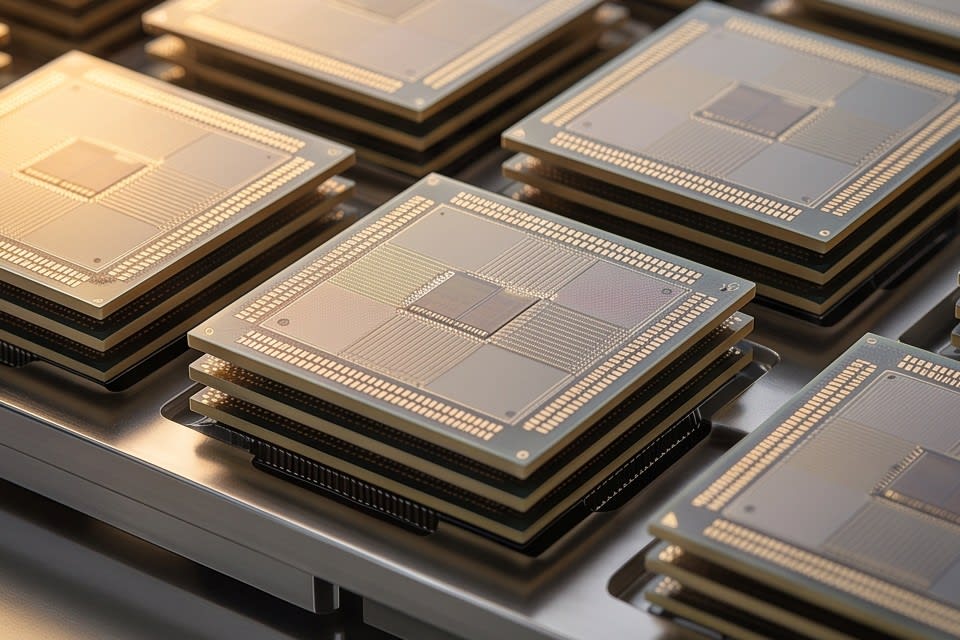
    View of multilayer stacked semiconductor packages arranged in rows

    Just a few years ago, thickness control in semiconductor packages was measured by whether they were thin enough. But as AI semiconductors and high-performance memory have become mainstream, the more important question has shifted to how uniform they are. As structures that stack chips in multiple layers have become common, even a single thickness deviation has emerged as a variable that can undermine the reliability of the entire package. As stacked structures become more complex, precision machining and cleaning technologies will become even more decisive standards for process quality.

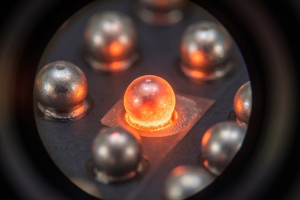
    View of solder microbumps placed inside a semiconductor package

    Why Thickness Uniformity Is a Key Quality Variable in Stacked Packaging

    In 3D IC packaging structures where chips are stacked vertically, thickness uniformity is not simply a dimensional issue. The solder microbumps that connect the chips between each layer repeatedly contract and expand during thermal cycling, and if there is variation in chip thickness, the stress distribution concentrated on the bumps changes. According to research published on ScienceDirect, thermal cycling tests of 3D IC packaging showed that creep in solder microbumps, plastic deformation caused by high-temperature load, can increase by up to 50%, directly affecting thermomechanical reliability.

    The greater the thickness deviation, the more stress becomes concentrated on specific bumps, and package warpage also worsens. As the number of stacked layers increases, the allowable tolerance range for each layer inevitably becomes narrower. When thickness nonuniformity in a single chip accumulates, the flatness of the entire package collapses, leading to bonding defects or electrical shorts in subsequent processes. In the end, thickness variation may not be visible, but it appears directly in the reliability metrics of the final product. As stacked packaging advances, securing thickness uniformity is becoming the starting point of process quality.

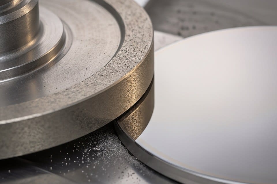
    View of a wafer or chip thickness being precisely machined using a diamond wheel

    Limitations of Conventional Machining Methods and the Role of Precision Grinding Technology

    Conventional grinding and chemical mechanical polishing have long been used as standards in semiconductor thinning processes, but their limitations are clear at the level of precision required by advanced packaging. According to an analysis by Eureka PatSnap, conventional grinding and chemical mechanical polishing processes often exceed thickness deviations of ±2μm, falling short of the latest package specifications that require submicron precision. As package types become more diverse, such as FCBGA, WLCSP, and QFN·DFN, and target thickness values vary, it is difficult for a single method to handle all specifications with the same level of precision.

    The moment deviation exceeds ±2μm, the package fails to meet the flatness criteria required in the next process, directly leading to yield loss. Micron-level grinding that combines a high-precision stage with a diamond wheel is one approach to closing this gap, and the same analysis shows that it can reduce material waste by 15 to 30% compared with conventional methods. Equipment such as a PKG Grinder, which supports both fully automatic and manual configurations, is designed to secure stable thickness precision in high-speed processes while maintaining production line flexibility. More important than which method is chosen is first defining the target package specification and allowable tolerance, then selecting the machining method that fits them.

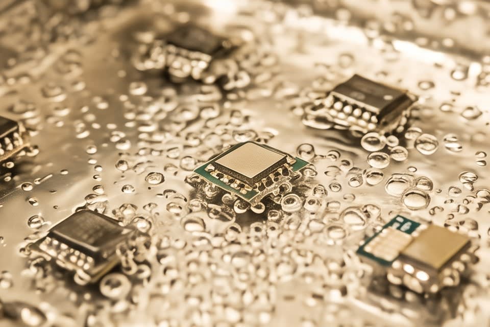
    View of fine water droplets formed on the surface of a semiconductor chip

    How the Cleaning Process Determines Final Quality

    If precision machining reduces thickness variation, the cleaning process determines the surface condition before the result moves on to the next stage. For components that require ultra-precision optical and electrical characteristics, such as camera modules or autonomous driving sensors, even a single fine particle left after grinding can result in a defect judgment. In the field, cleaning is often regarded as the last step, but in practice it is the process that determines final quality.

    According to research published in MDPI, cleaning solutions containing micro-nano bubbles improve the photoresist removal rate by 30%. A multistage cleaning method that applies Micro Bubble, Water Jet, and Air Knife step by step is structured to separate and discharge contaminant particles at each stage that are difficult to remove with a single method. For parts with complex shapes, such as VCM motors or semiconductor trays, the combination and sequence design of cleaning methods directly affect removal efficiency. When residual moisture is also removed through the Oven Dry process after cleaning, the possibility of secondary contamination in subsequent assembly or inspection processes is reduced.

    Lower defect rates and stable yield ultimately come from how precisely the surface is controlled at this cleaning stage. The fact that invisible particles determine the quality of the entire process becomes clear the moment cleaning results are connected to shipping quality.

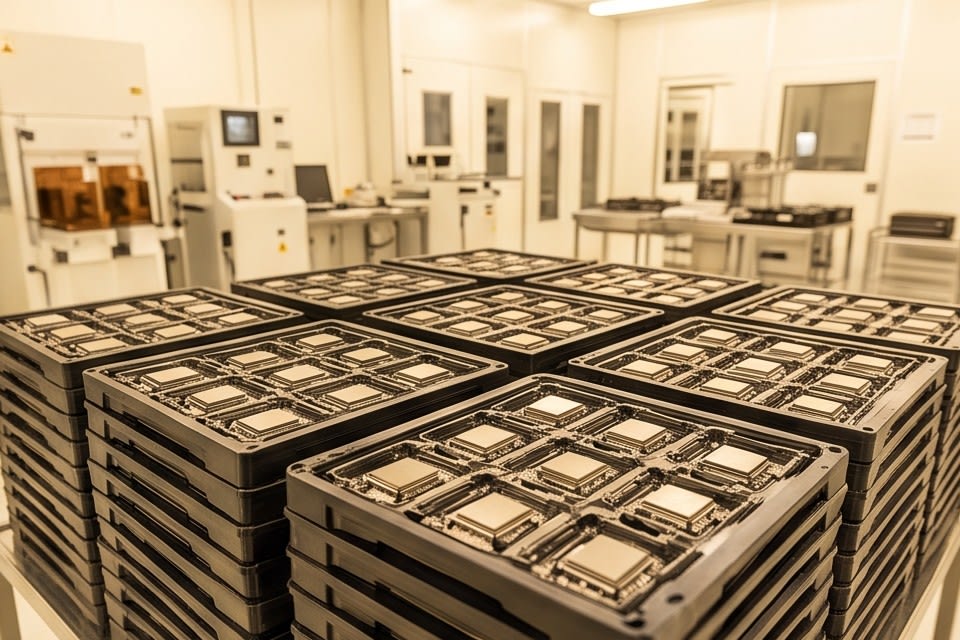
    View of cleaned semiconductor components aligned and loaded on trays

    Reducing defects in semiconductor processes is not a matter of just one step. Package reliability is secured only when two processes work together: precision grinding that controls thickness variation at the micron level, and multistage cleaning that removes surface contaminant particles step by step. In a structure where the precision of each individual process determines the yield and reliability of the final product, which technologies are selected and how they are combined become practical benchmarks of manufacturing competitiveness.


    Huvics is an advanced technology company that develops and manufactures automation equipment and
    production systems across the semiconductor, LED, Mobile, and Cosmetic industries.
    With top talent and continuous technological innovation, we help customers improve productivity and
    secure quality competitiveness.

    Huvics Contact

    Tel: 031-374-8285
    Email: cdpark@huvics.com

    Huvics Inquiry

  • 3 Core Technologies of the Huvics One Stop Laminator System That Improve Semiconductor Process Efficiency

    3 Core Technologies of the Huvics One Stop Laminator System That Improve Semiconductor Process Efficiency

    Huvics

    A semiconductor manufacturing site is an intensely competitive battlefield where every minute and every second of efficiency becomes technological competitiveness. In a semiconductor line where countless micro processes operate in close coordination, improving process efficiency is a core indicator that determines a company’s competitiveness.

    Until now, many production sites have handled the essential processes of tape mounting and ultraviolet curing independently using separate equipment. However, this separated operation method has created invisible barriers, including lead time caused by movement between facilities and the inconvenience of management.

    Huvics One Stop Laminator System

    Innovation of the One Stop Laminator System

    Huvics presents an innovative solution called the One Stop Laminator System to address these structural challenges in semiconductor manufacturing processes. By integrating previously separated process steps into one, it boldly removes the physical gaps that had hindered manufacturing efficiency. The key features of this system are as follows.

    • Supports both lamp type and LED type ultraviolet curing systems
    • Offers precision control capabilities optimized for the characteristics of each film
    • Prevents damage to heat-sensitive components through process simplification

    One Stop Process Flow Diagram

    Extreme Precision Control Technology

    The point where Huvics technology stands out most in the field lies in its precision control capability that maintains extreme levels of detail. The various adhesive films used in semiconductor back-end processes require different curing conditions depending on the type.

    The Huvics system is designed to finely adjust the optimal irradiation intensity for each difficult-to-handle film. In a semiconductor environment where even the smallest variable cannot be tolerated, this precision control system becomes an essential element for ensuring stable quality.

    Precision Ultraviolet Curing Module

    Maximizing Process Stability and Production Yield

    Electronic components that are especially sensitive to heat can be at risk of physical deformation from even slight temperature changes. Through its distinctive cooling and output control technologies, Huvics fundamentally prevents substrate damage and maximizes process stability. This meticulous process management delivers the following results.

    • Improves process efficiency beyond simply reducing defect rates
    • Provides customers with a higher level of production yield
    • Becomes the foundation for building a stable process environment

    Smart Control Panel

    The power to break down the complex barriers of semiconductor manufacturing comes from the simplicity of removing unnecessary steps and the precision that fills the process. The Huvics One Stop Laminator System is a technological achievement completed after relentless efforts to pursue efficiency, promising customers flawless process stability and dramatic yield improvement.

    When it is time to secure both production speed and product value, the technological completeness of Huvics will provide the most reliable support for your site.


    Huvics is an advanced technology company that develops and manufactures automation equipment and
    production systems across the semiconductor, LED, Mobile, and Cosmetic industries.
    With top-tier talent and continuous technological innovation, we support customers in improving productivity and
    securing quality competitiveness.

    Huvics Contact Information

    Phone: 031-374-8285
    Email: cdpark@huvics.com

    Huvics Inquiry

  • Huvics High Precision PKG Grinder – Solving Technical Challenges in Semiconductor Processes and Strategies for Maximizing Production Efficiency

    Huvics High Precision PKG Grinder – Solving Technical Challenges in Semiconductor Processes and Strategies for Maximizing Production Efficiency

    Huvics

    As the next generation semiconductor market becomes more advanced, the technical precision required on the production floor has reached an extraordinary level. In particular, securing micron level thickness uniformity and flatness in the production of high performance memory and semiconductors for artificial intelligence has become a core challenge that determines product quality and corporate competitiveness.

    To overcome these challenges, Huvics is setting a new standard with a high precision packaging grinder that combines proprietary ultra precision grinding technology with optimized diamond wheels. This article explores the strategic value of the Huvics system, which responds flexibly to production scale and site conditions, maximizing manufacturing process efficiency and supporting solid business competitiveness.

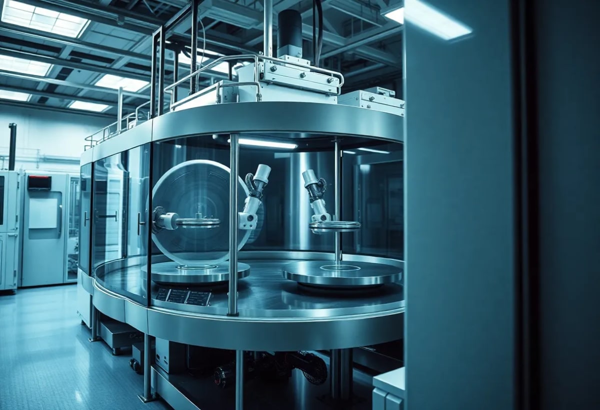
    Cleanroom view showing the reliability of the semiconductor process

    Technical Challenges in Semiconductor Processes and Their Solutions

    The Importance of Ultra Precision Grinding Technology

    As the semiconductor industry continues to advance, the technical barriers encountered on the production floor are becoming increasingly high. In particular, securing thickness uniformity and flatness in the manufacturing of next generation semiconductors and high performance memory is a key task that determines final product quality. In a strict environment where even the slightest error cannot be allowed, overcoming these physical limits goes beyond a simple technical achievement and becomes a decisive factor that separates market leaders from the rest.

    The Role of the Huvics Packaging Grinder

    At a point where many manufacturers are seeking ways to improve process reliability, Huvics presents a new solution through a high precision packaging grinder that combines proprietary ultra precision grinding technology with optimized diamond wheels. This equipment goes beyond a simple processing tool and serves as a powerful engine that fundamentally improves the quality of high value semiconductor products by perfectly controlling fine tolerances at the micron level. For companies seeking to break through technical challenges head on, the Huvics system will become the clearest milestone for building a stable manufacturing environment.

    Diamond wheel integrating ultra precision grinding technology

    Customized Solutions That Maximize Production Efficiency

    Site Specific Process Design

    Semiconductor manufacturing sites are dynamic environments that must respond quickly to rapidly changing market demand. When production scale increases, large scale automated lines are required, but flexible manual processes may also be needed for research and development or high mix low volume production. The Huvics PKG Grinder was designed to carefully reflect these production site needs.

    Key Benefits of the Huvics System

    A major feature is its customized solution structure, which can respond flexibly regardless of producer scale or individual manufacturing conditions. The key benefits provided by the Huvics system are as follows.

    • Maximizes production speed by building a fully automated process line
    • Improves capital efficiency by selecting a manual configuration when needed
    • Greatly improves process changeover speed to respond quickly to market changes

    This goes beyond simply introducing equipment and becomes a strategic foundation that enables manufacturers to find optimal process efficiency and secure a competitive edge in the fast changing semiconductor market. The customized configuration pursued by Huvics significantly reduces trial and error that may occur on site, steadily improves production yield, and helps companies continue a stronger business journey.

    Enhancing corporate productivity through top level performance and a flexible system, that is the essence of the partnership Huvics pursues.

    Refined technology providing customer tailored solutions

    As technical barriers in semiconductor manufacturing continue to rise, overcoming minute errors and securing production flexibility have become essential tasks that determine a company’s future competitiveness. Based on ultra precision grinding technology, Huvics provides complete process control and customized solutions, becoming more than an equipment supplier and serving as the most reliable partner to help your business enter a stable growth trajectory.

    If you want to improve process reliability and secure differentiated manufacturing competitiveness amid rapidly changing market demands, we invite you to find the answer to optimized process efficiency with Huvics.


    Huvics is an advanced technology company that develops and manufactures automation equipment and
    production systems across the semiconductor, LED, Mobile, Cosmetic industries.
    With top talent and continuous technological innovation, we support customers in improving productivity and
    securing quality competitiveness.

    Huvics Contact

    Phone: 031-374-8285
    Email: cdpark@huvics.com
    Huvics Inquiry

  • Huvics High-Performance Laminator-4 Key Strategies for Semiconductor Production Efficiency and Process Optimization

    Huvics High-Performance Laminator-4 Key Strategies for Semiconductor Production Efficiency and Process Optimization

    Huvics

    In semiconductor manufacturing, process efficiency is the most critical indicator that determines a company’s competitiveness. On manufacturing lines where numerous systems are arranged in dense configurations, even a very small waste of time or minor spatial inefficiency can create a significant difference in the quality and output of the final product.

    Huvics precisely addresses these demanding needs in industrial production sites and introduces a next-generation high-performance laminator lineup designed to dramatically maximize semiconductor production efficiency.

    Precision drive unit of a high-performance laminator

    Innovation in Integrated Process Systems

    Huvics has built an innovative all-in-one system that brings together previously fragmented tasks, including lamination, tape mounting, and ultraviolet curing processes, into one organic framework. The key features of the integrated solution provided by Huvics are as follows.

    • One-stop support from expander to ultraviolet curing
    • Dramatically shortens the overall takt time of the production line
    • Provides flexible automation options tailored to customer environments
    • Optimizes the footprint occupied by equipment

    Solving Bottlenecks and Optimizing Processes

    The true value of the Huvics high-performance laminator system goes beyond the physical simplification of processes. It lies in fundamentally resolving bottlenecks that commonly occur across the entire production line. Unnecessary waiting time and frequent movement between processes are major factors that hinder productivity in manufacturing environments.

    However, the Huvics solution seamlessly connects these stages and becomes a powerful core driver that organically controls the flow of the entire line.

    Organically integrated process system

    Maximizing Automation and Operational Efficiency

    In particular, automation options that can be flexibly selected according to the different environments and requirements of each site help companies respond immediately to rapidly changing production issues. By internalizing complex manual tasks that previously required substantial manpower and designing optimized workflow paths, operators can reduce the effort required for equipment operation.

    Managers can now move away from simple repetitive tasks and enjoy a more comfortable environment where they can focus on the essence of production. This technological advancement goes beyond increasing speed. It helps prevent potential risks that may arise in advanced semiconductor processes and maximizes the stability of the entire line.

    User-centered intuitive control panel

    Enhancing Space Utilization and Production Capacity

    One of the most valuable and strategic resources in semiconductor manufacturing is space. The Huvics laminator is designed to precisely analyze and optimize equipment footprint, maximizing space utilization even within limited production lines.

    Efficient use of space directly means the potential for line expansion, which is closely connected to strengthening a company’s long-term production capacity. Combined with an intuitive interface and an innovative system structure, it significantly reduces dependence on operator skill while ensuring stable and reliable process performance.

    Equipment layout that maximizes space efficiency

    The ability to operate the system efficiently even without highly skilled field technicians greatly increases flexibility in workforce management and helps maintain process consistency. The Huvics all-in-one lamination system goes beyond the introduction of simple equipment and is establishing itself as a key strategic partner that structurally reduces customer production costs and drives sustainable profitability improvement.

    Huvics is redefining the efficiency of manufacturing processes through technology, drawing strong attention in the global manufacturing market and setting a new standard for semiconductor production. This innovation goes beyond simple efficiency and presents the right direction for the semiconductor industry to move forward.


    Huvics is an advanced technology company that develops and manufactures automation equipment and
    production systems across the semiconductor, LED, mobile, and cosmetic industries.
    With top-tier talent and continuous technological innovation, Huvics supports customers in improving productivity and
    securing quality competitiveness.

    Huvics Contact Information

    Tel: 031-374-8285
    Email: cdpark@huvics.com
    Huvics Inquiry

  • Three Key Steps to Why Global Semiconductor Leaders Choose Huvics’ Process Analysis

    Three Key Steps to Why Global Semiconductor Leaders Choose Huvics’ Process Analysis

    Huvics

    According to the 2023 ‘Tech Insight’ report by a leading global semiconductor industry research institution, over 30% of companies purchasing advanced semiconductor equipment struggle to improve productivity due to insufficient pre-process analysis. This clearly shows that merely adopting high-cost equipment, costing billions of won, does not guarantee optimization of the entire complex manufacturing process. For global semiconductor leaders to turn massive investments into successful business outcomes, the role of specialized companies that can conduct in-depth analysis of the entire process and suggest optimal solutions before equipment purchase is more crucial than ever. Huvics goes beyond merely supplying equipment, acting as a reliable partner in kickstarting this crucial first step for the successful business journey of our clients.

    Grand Semiconductor Equipment, Strategic Investment

    Eliminating Uncertainty for Strategic Investment

    The primary reason global semiconductor manufacturing companies turn to Huvics before purchasing high-tech equipment worth billions is due to the necessity of expert involvement to eliminate uncertainty and lead strategic investments to success. Merely introducing high-cost equipment does not guarantee optimization of the entire intricately linked manufacturing process. Predicting how new equipment will synergize with existing production lines, its impact on yield, and its adaptability to rapidly changing technological environments is challenging without in-depth pre-analysis. Such uncertainties translate into enormous financial risk and become strategic decisions that influence the success or failure of the entire production system. At such a crucial juncture, Huvics helps dispel uncertainties stemming from the complexities unique to the semiconductor industry and the significance of equipment choice by offering a clear data-driven roadmap, allowing our clients to stride toward a better future.

    Huvics

    In-depth Analysis and Tailored Solutions for the Entire Manufacturing Process

    The second core reason semiconductor companies trust Huvics to eliminate uncertainty lies in Huvics’ unique ‘in-depth analysis of the entire manufacturing process’ approach. Huvics moves beyond a myopic view of merely examining individual equipment performance metrics and specifications.

    Instead, Huvics thoroughly assesses how the entire production line, with its numerous interconnected equipment and processes, operates, spots potential inefficiencies, and unveils hidden opportunities for optimization. By gathering and analyzing vast amounts of data from multiple angles, Huvics precisely identifies unnoticed bottlenecks and clearly extracts potential areas for improvement that may have gone unseen.

    The deeply derived analysis results are implemented as customized total solutions perfectly tailored to the unique production environment of the client and their specific goals. This transcends merely replacing a single piece of equipment, offering a practical roadmap that maximizes production efficiency and encompasses future-oriented growth strategies. Just like a precise health checkup realigns the body, Huvics diagnoses the health of semiconductor processes and prescribes the optimal treatment.

    Cleanroom, Precise Process Diagnosis

    Close Technical Support for Successful Implementation

    Huvics’ value doesn’t end at proposing solutions; it truly shines in the third and most important step—’successful implementation through close technical support.’ Huvics spares no effort to ensure that the proposed solutions are successfully implemented in the actual production field. Even after equipment introduction, Huvics operates a continuous monitoring system to observe even the slightest changes in the production line and proactively identifies and resolves unexpected issues or improvements through careful feedback with clients. Such comprehensive technical support enables clients not only to achieve expected productivity enhancements but also reduces operating costs, improves quality, and ultimately secures continual technological innovation and robust market competitiveness, laying the groundwork for long-term value. Huvics evolves into a key partner, not a one-time transaction, keeping pace with clients to continually maximize production efficiency and drive future growth. Consequently, Huvics firmly establishes itself not just as an equipment supplier but as an indispensable partner and essential success factor in the successful business journeys of global semiconductor leaders.

    Robotic Arm, Precise Automation Implementation

    In the semiconductor industry, where investments of billions are at stake, equipment selection goes beyond simple purchases to become critical strategic decisions that dictate a company’s future. At this critical juncture, Huvics eliminates uncertainty with a systematic three-step approach from data-driven in-depth process analysis to proposing tailored solutions and providing close technical support for successful implementation. Huvics establishes itself as a reliable partner that helps global semiconductor leaders optimize complex manufacturing processes and continuously innovate to secure sustainable competitive advantage. Partnership with Huvics will become an essential driving force for the future success of the semiconductor industry.


    Huvics is an advanced technology company developing and manufacturing automation equipment and production systems spanning Semiconductor, LED, Mobile, and Cosmetic industries.
    We support increased productivity and quality competitiveness with top talent and ongoing technological innovation.

    Huvics Co., Ltd Contact

    Phone: 031-374-8285
    Email: cdpark@huvics.com
    Huvics Inquiry

  • Huvics Semiconductor Equipment Tackles Defect Rates with 3 Successful Field Case Studies

    Huvics Semiconductor Equipment Tackles Defect Rates with 3 Successful Field Case Studies

    According to recent trends in the semiconductor industry, an increase of just 1% in defect rates in more miniaturized processes can cause losses amounting to billions. This issue goes beyond simply reducing production volume, posing a significant threat to the overall efficiency of complex manufacturing lines and product reliability. The modern semiconductor manufacturing field is facing the tremendous wave of endless miniaturization and increased complexity, with defect rate management, once unimaginable in the past, now becoming the biggest challenge. It has reached a point where existing equipment can no longer ensure stable yield, leading to a grave situation that threatens not only productivity but also the reliability of the final product. Thus, solving these challenges and securing stable yields have become urgent tasks for all semiconductor manufacturers, making the introduction of new equipment for building next-generation semiconductor production lines—requiring high precision and perfect cleanliness—not just an option but a necessity. At this juncture, Huvics is opening new horizons in semiconductor production by addressing chronic defect rate issues with innovative equipment solutions.

    Precision Grinding Technology-Based Innovation by Grinder System

    Micron-Level Precision Machining Technology

    Huvics’s core solution, the precision grinding technology-based Grinder System and PKG Grinder, is at the forefront of change. These machines handle wafers or packages with a precision that does not tolerate even micron-level errors. By processing various packages such as FCBGA, WLCSP, QFN/DFN, and Solar Cells to perfectly uniform and precise specific thicknesses as required by customers, they play a crucial role in fundamentally blocking the possibility of physical defects that can occur in fine processes and securing stable yields.

    The core of semiconductor production lies in error-free precision and unchanging perfection. Micron-level slight thickness variations often lead to critical defects affecting productivity and profitability. Huvics deeply understands these field difficulties and presents solutions with its precision grinding technology-based grinder system and PKG grinder. In fact, after adopting the Huvics system, one major semiconductor manufacturer noticeably improved the defect rate caused by slight thickness variations in the FCBGA package process, elevating production efficiency to a new level.

    Flexible Production Line Configuration and Response

    Furthermore, the flexible production line configuration ability of Huvics equipment provides optimized solutions for diverse production environments. By selectively combining fully automated Full Auto types with Manual types that require detailed control by skilled operators, it actively responds to changing production demands and technological advancements. This provides a solid foundation that perfectly complies with product specifications even in the precision processing of complex packages, strengthening the market competitiveness of client companies.

    Perfect Contamination Removal with Advanced Cleaner Machines

    The Threat of Fine Contamination and Need for Solutions

    Particles or contaminants that may finely remain after micron-level precise grinding processes often result in critical defects in the final product quality. If invisible contaminations remain, no matter how precisely processed, the efforts can be in vain. This ‘invisible threat’ was one of the most challenging obstacles in managing defect rates in semiconductor manufacturing. Huvics took a deep interest in this issue and developed an innovative cleaner machine solution that uproots contamination, going beyond just wiping away, introducing it to the field.

    Multi-Stage Cleaning Technology and Quality Stability

    Huvics’s cleaner machine showcases the essence of advanced multi-stage cleaning technology. By integrating micro-bubble, powerful waterjet, and precise air knife technologies, it leaves no room for fine contamination particles sticking to product surfaces. It provides optimized cleaning protocols considering the properties of sensitive high-value-added components like camera modules and sensors, adding an oven dry function to completely block the possibility of secondary contamination occurring in the final drying process. In fact, many customers have seen a noticeable reduction in defect rates due to fine contamination, significantly improving quality stability and production efficiency after adopting the cleaner machine.

    Successful Field Case Studies of Huvics Solutions

    In semiconductor production fields, defect rate management is becoming increasingly important with the complication of micro-processes. Amidst this backdrop, Huvics has drastically reduced defect rates through innovative equipment solutions across numerous fields, achieving stable target yields, and leading a successful transformation. Now we’ll specifically explore three key field cases showing how Huvics’s advanced equipment presents new standards for semiconductor manufacturing, from micron-level precision machining to perfect multi-stage cleaning.

    1. Significantly reduced defect rates and improved product reliability in precision package processing with PKG Grinder.
    2. Notably lowered defect rates in wafer and product cleaning sites by removing fine contamination particles with Cleaner Machine adoption.
    3. Established flexible production lines and achieved stable target yields by integrating the operation of grinders and cleaner machines.

    Facing the massive wave of precision and complexity deepening, the defect rate issue in semiconductor manufacturing fields has become an essential task that can no longer be overlooked. Today, we could confirm through three cases how Huvics’s advanced equipment has drastically reduced defect rates and secured stable yields in the field, from micron-level precision processing to perfect multi-stage cleaning. This goes beyond just increasing efficiency to fundamentally strengthen the reliability of semiconductor production, becoming an important indicator determining future competitiveness. Huvics’s technological evolution, as such, will open new horizons for the semiconductor industry through visible outcomes.


    Huvics is an advanced technology company that develops and manufactures automation equipment and production systems across industries such as semiconductors, LED, mobile, and cosmetics.
    We support our customers’ productivity enhancement and quality competitiveness through top-tier talent and continuous technological innovation.

    Contact Huvics

    Phone: 031-374-8285
    Email: cdpark@huvics.com
    Contact Huvics

  • Why Cleaner Equipment Management Determines Productivity and Quality

    Why Cleaner Equipment Management Determines Productivity and Quality

    In the semiconductor and advanced electronic component industries, cleaner equipment is like an essential facility that requires meticulous management. It is because they are sensitive to even tiny dust particles, minor temperature changes, and changes in the concentration of cleaning solutions, which can impact the quality of the entire production line.

    Just as a baby’s health requires meticulous care, cleaner equipment also needs regular inspections and maintenance to maintain optimal performance. This not only extends the life of the equipment but also contributes to enhancing the overall stability and efficiency of the production process. Let us now delve deeper into understanding cleaner equipment and reveal key management methods to boost productivity.

    Core Component Management: The Importance of Regular Health Checkups

    Managing the core components of cleaner equipment is like conducting health checkups for our bodies. Just as early detection and management of abnormal signs can prevent major illnesses, periodically inspecting and cleaning the main components of the equipment can extend its life and maintain optimal performance.

    For example, failing to replace a car’s engine oil on time can damage the entire engine. Similarly, if you do not replace filters or nozzles on cleaner equipment at the right time, the cleaning effect can decrease, and it could cause malfunction. Setting regular inspection cycles and learning how to clean and replace each part is the most fundamental first step in equipment management.

    Cleaning Solution Management: The Recipe for Best Results

    Cleaning solution management is like a chef meticulously adjusting the freshness and ratios of ingredients to achieve the best taste. No matter how good the ingredients, if the ratios are incorrect or freshness declines, a great dish cannot be made. Similarly, cleaner equipment also struggles to perform at its best if cleaning solution management is neglected.

    The concentration, temperature, and pH concentration of the cleaning solution are key factors that directly impact cleaning quality. If these conditions aren’t maintained in an optimal state, the cleaning power may decrease, leading to a higher defect rate in products. Therefore, regularly inspecting and managing the cleaning solution plays a crucial role in enhancing the efficiency and quality of the entire production process.

    Identifying Abnormal Symptoms: Listening to the Signals from Equipment

    Small noises or changes occurring in cleaner equipment are like subtle pain signals from our bodies. Strange noises, vibrations, or sudden temperature changes may indicate an issue inside the equipment.

    If you ignore and neglect these signals, a minor problem can escalate into major damage that halts the entire production line. Just as a skilled mechanic pays attention to minor sounds in a car to identify potential problems, it is important not to overlook small changes in equipment. This is a wise method to extend the equipment’s life and maintain stable production.

    The management of cleaner equipment requires consistent attention, much like caring for a delicate baby, but it rewards with definite results. The core component management, cleaning solution management, and identifying abnormal symptoms discussed today are essential elements in extending equipment life and maximizing productivity. With this systematic management, we hope the cleaner equipment always maintains the best condition and becomes a reliable partner for your company.

    Huvics is a high-tech innovation company that develops and manufactures automation equipment and production systems across semiconductor, LED, Mobile, and Cosmetic industries.
    We support enhancing customer productivity and securing quality competitiveness through outstanding talent and continuous technological innovation.

    Contact Huvics Co., Ltd.

    Phone: 031-374-8285
    Email: huvics01@gmail.com
    Contact Huvics