Tag: technology innovation

  • 3 Process Points That Prevent Semiconductor Defects – Key Summary of Grinding, Lamination, and Cleaning

    3 Process Points That Prevent Semiconductor Defects – Key Summary of Grinding, Lamination, and Cleaning

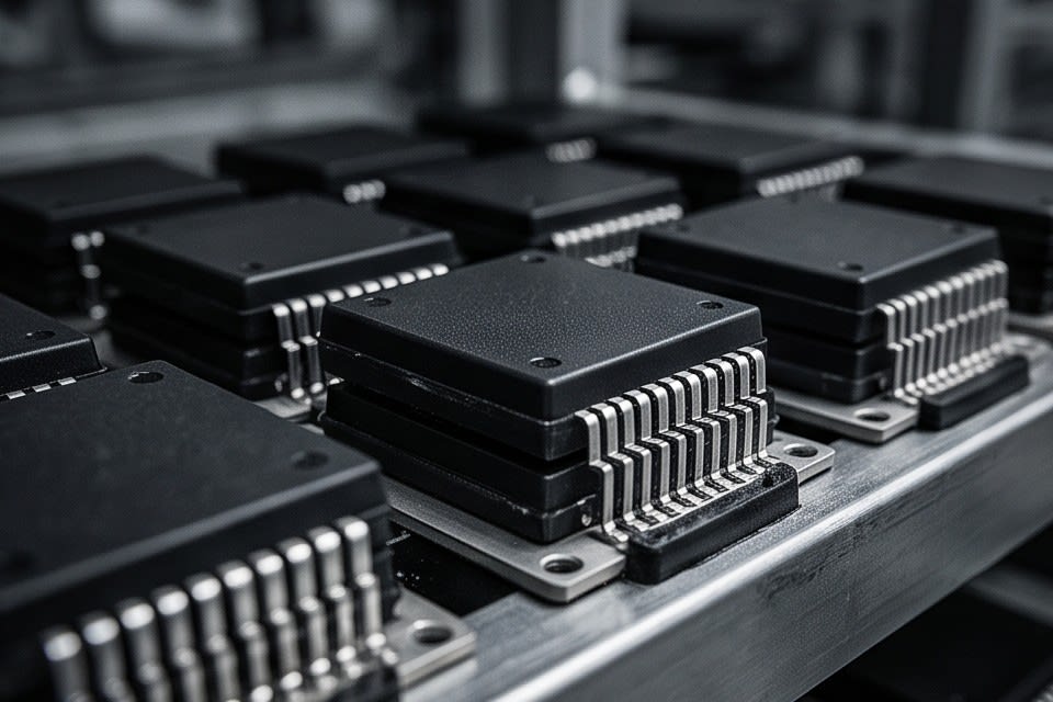
    A completed chip semiconductor packaging component after vertical stacking and lead frame alignment

    If defects are found in parts after cleaning, the loss has already started somewhere in the process. Thickness variation in the grinding stage, uneven adhesion in the tape attachment process, contamination residue remaining after cleaning — if even one of these three issues is overlooked, yield loss and rework costs can grow rapidly. The later a problem appears in the downstream process, the more correction costs increase exponentially, and delayed delivery can even undermine customer trust.

    A smoothly processed circular wafer placed on equipment with tolerances of less than 1 micron

    Thickness Uniformity in the Grinding Process Determines Yield

    In the semiconductor packaging process, thickness uniformity is one of the most sensitive variables that determines yield. Modern package structures such as WLCSP wafer level chip scale package, FCBGA, and QFN are based on vertical chip stacking, and if the thickness after grinding is even slightly uneven, stacking chips on top becomes impossible.

    According to analysis by AE Research, the thickness uniformity tolerance required in semiconductor grinding processes is less than 1 micron, and chips outside this standard immediately lead to defects in the stacking process. This is why micron level precision grinding using diamond wheels is not simply a machining technology, but a prerequisite for package reliability. To maintain this level of tolerance consistently even in high speed processes, stage precision and consistent grinding conditions must both be secured. Keeping thickness variation within the allowable range is the key to high yield production.

    A lamination film attachment process applying tape evenly to a wafer surface with a roller

    Integrated Lamination Processes Prevent Error Accumulation

    The more a process is divided into multiple stages, the more errors accumulate between each stage. When tape attachment, UV curing, and expanding are performed on separate equipment, alignment can shift or adhesion conditions can vary during transfer between processes.

    The laminator system from Huvics structurally prevents this issue by integrating key processes from the expander to UV curing within a single system. In the UV curing stage, uniform irradiation intensity is especially important. Uneven UV irradiation causes film shrinkage and adhesion variation, increasing the risk of damage in the subsequent chip separation process. In contrast, when UV curing is performed under controlled conditions, tape adhesion weakens predictably, allowing chips to be separated without damage.

    A UV curing system that can selectively apply lamp and LED methods provides the flexibility to respond according to product type and production volume. Connecting processes into one continuous flow and reducing the number of transfers is itself implemented as a way to secure both shorter takt time and process stability.

    High pressure water jets sprayed from nozzles to remove foreign particles from the surface of semiconductor components

    The Cleaning Process Is the Final Gateway to Quality

    No matter how precise the machining and attachment processes are, final quality becomes unstable if contaminants remaining on the surface are not removed. In camera module manufacturing sites, if residual flux and contamination particles generated during the reflow process after CSP assembly are not removed through cleaning, ionic residues cause corrosion and directly affect module performance.

    In production environments that handle components with diverse shapes and materials, such as VCM motors, image sensors, and trays, a single cleaning method makes it difficult to respond to all types of contamination. The cleaner system from Huvics removes surface contamination particles step by step through a multi stage cleaning method that combines micro bubbles, water jet, and air knife, and it also includes an oven drying function to remove residual moisture after cleaning.

    Full auto and manual methods can be selected, allowing flexible application depending on the line configuration. In automated configurations, worker intervention between processes is minimized, reducing the risk of contamination reattachment. In the field, results show that as the defect rate in the cleaning stage decreases, the downstream rework rate also drops.

    A continuous process line where semiconductor components are transferred along a conveyor belt in an automated system

    Micron level precision in the grinding process, an integrated flow in the lamination process, and multi stage contamination removal in the cleaning process — these three elements are not separate technologies, but one connected line of defense against semiconductor defects. Weakness in any one stage is transferred as a burden to the next stage, and the structure in which it is ultimately confirmed as a defect in final inspection will inevitably repeat unless the entire process is designed with precision. Controlling variation at each point in the process is a far more cost effective way to protect quality than tracing the cause after a defect occurs.


    Huvics is an advanced technology company that develops and manufactures automation equipment and
    production systems across the semiconductor, LED, Mobile, and Cosmetic industries.
    With top talent and continuous technological innovation, we support customer productivity improvement and
    quality competitiveness.

    Huvics Contact

    Phone: 031-374-8285
    Email: cdpark@huvics.com

    Contact Huvics

  • How to Improve Semiconductor Packaging Process Efficiency and Quality Stability with the Huvics Laminator System

    How to Improve Semiconductor Packaging Process Efficiency and Quality Stability with the Huvics Laminator System

    Huvics

    As semiconductor packaging technology advances rapidly and demands even higher precision, overcoming process limitations has become not a choice but a matter of survival. In particular, inefficient waiting time and physical movement caused by segmented steps from cleaning to assembly remain unresolved challenges for site managers who must increase productivity.

    Is it possible to create an ideal process environment that integrates complex steps while maintaining quality reliability? The one-stop laminator system proposed by Huvics is the answer to this challenge, fundamentally changing the paradigm of manufacturing sites by organically integrating process flow.

    Robotic arm improving efficiency through automation

    A One-Stop System That Improves Semiconductor Process Efficiency

    Stacked Packaging and Process Challenges

    The modern semiconductor industry requires a higher level of precision than ever before. In particular, as stacked packaging technology advances dramatically, the accuracy of the process that stably builds numerous layers has become a key competitive advantage that determines a company’s market share.

    In this environment, semiconductor assembly sites face even more demanding challenges. Conventional cleaning and assembly processes are separated by each step, causing repeated physical movement and waiting time, which inevitably leads to inefficient takt time and hinders productivity improvement.

    Huvics Integrated Laminator Innovation

    Huvics provides the answer at this exact point. Beyond simply advancing individual equipment, its one-stop laminator combines tape mounting and UV curing technology into one original system.

    From expansion to the final stage of UV curing, Huvics innovation processes every step continuously within a single piece of equipment, overcoming existing physical limitations at once and opening a new paradigm in process efficiency.

    Precisely seated wafer process

    Quality Stabilization Through Precision UV Curing Technology

    Adhesion Strength Control and Defect Prevention

    The reason the Huvics one-stop laminator system receives outstanding evaluations in the field is not only that it physically integrates the process flow. Behind it lies the technological essence of a precision UV curing mechanism that strategically combines lamps and LEDs.

    Controlling the adhesion strength of tape during the semiconductor packaging process is a highly sensitive task that determines the stability of the final product. If adhesion is too strong, it can damage devices during removal, and if it is too weak, it can cause defects such as misalignment during the process.

    Implementation of precision UV curing technology

    Improved Reliability of the Production Line

    The Huvics system finely controls this adhesion strength to maintain the optimal condition. This precise control technology functions as a safeguard that blocks potential defect factors that may occur during production at the source.

    As a result, site managers can reduce anxiety about defect rates and operate production lines in a much more stable environment. This is not simply a replacement of equipment, but a strategic investment that fundamentally raises the reliability of manufacturing quality to a higher standard.

    Huvics

    Securing Market Competitiveness Through Technological Completeness

    Consistent Process Results and Efficiency

    At semiconductor manufacturing sites, quality reliability is directly connected to customer trust. Huvics technology systematically ensures the completeness of the entire process, from the cleaning process to subsequent assembly stages.

    Unlike past methods that required countless trials and errors to meet demanding process conditions, the integrated system from Huvics delivers consistent results. In particular, the LED-based UV curing environment maximizes energy efficiency while ensuring uniform curing performance, raising product reliability to the highest level.

    A Production Line Optimization Partner

    For companies, this kind of technological stability becomes the strongest foundation for securing unwavering competitiveness in the market. Maintaining high yields without defects while responding flexibly to the rapidly changing demands of the semiconductor market, Huvics realizes this ideal manufacturing site and establishes itself as a powerful partner that optimizes production line operations beyond the role of a simple supplier.

    Production site of a smart factory

    Integrated Solutions for Future Manufacturing Sites

    An Engine for Maximizing Productivity

    In conclusion, the one-stop laminator system from Huvics is the optimal engine for solving the long-standing corporate goal of maximizing productivity. It dramatically reduces waiting time between process stages and minimizes the possibility of human error through automated precision control, maximizing on-site efficiency.

    This goes beyond simply reducing costs and organically improves the flow of the entire process, enabling resilient responsiveness to future changes in the technology environment. In an environment where stacked packaging technology continues to advance, this kind of technological choice that secures both process efficiency and quality stability is essential.

    Advanced semiconductor manufacturing cleanroom

    Enhancing Business Value

    This integrated solution proposed by Huvics clearly shows the direction semiconductor manufacturing sites should take. If your company seeks to build a defect-free production system based on high technological completeness, elevate your business to the next level through the innovative process integration engine from Huvics.

    As semiconductor processes become more complex, the flexibility and precision to connect segmented stages into one have become key values that determine corporate survival beyond simple competitiveness. The one-stop laminator system from Huvics breaks down the walls of inefficiency that hinder production flow and presents a technological milestone that raises the completeness of the entire process to the next level.

    At today’s manufacturing sites that demand advanced precision, design the future of your process through a proven integrated solution instead of worrying about unnecessary waiting and defects. The unwavering stability realized by Huvics will bring optimal efficiency and trust to your production line.


    Huvics is an advanced technology company that develops and manufactures automation equipment and
    production systems across the semiconductor, LED, Mobile, and Cosmetic industries.
    With outstanding talent and continuous technological innovation, we support customer productivity improvement and
    quality competitiveness.

    Huvics Contact

    Phone: 031-374-8285
    Email: cdpark@huvics.com

    Huvics Inquiry

  • Semiconductor Back-End Process Innovation—Quality Reliability Achieved with Huvics Ultrasonic Dispersion and Precision Vision Inspection Solutions

    Semiconductor Back-End Process Innovation—Quality Reliability Achieved with Huvics Ultrasonic Dispersion and Precision Vision Inspection Solutions

    Huvics

    As semiconductors and electronic components enter an era of ultra-high integration that pushes beyond previous limits, even the smallest variables arising during the manufacturing process are becoming critical risks that determine the fate of finished products. In particular, controlling microscopic pattern distortion and foreign particles that cannot even be identified with the naked eye in advanced component production sites such as flexible printed circuit boards and multilayer ceramic capacitors is a core challenge that determines corporate survival.

    Recently, Huvics has been presenting a new standard in the back-end process field by directly addressing technical challenges with a unique convergence solution that combines ultrasonic energy and intelligent vision algorithms.

    Ultra-Precision Process Control Technology

    Quality Risks in the Era of High Integration and the Huvics Solution

    The semiconductor and electronic component markets are moving toward high integration that surpasses technological limits even at this moment. An era has arrived in which microscopic circuits and complex structures that were difficult to imagine in the past are naturally installed in everyday smart devices.

    Amid this trend, technology that controls minute quality variations in the back-end process field has become an absolute competitive advantage that determines the success or failure of companies. Huvics presents a unique technical solution to resolve quality risks that frequently occur in multilayer ceramic capacitor and flexible printed circuit board processes.

    Convergence of Ultrasonic and Vision Technology

    The core capability of Huvics begins with using ultrasonic energy to uniformly disperse key material particles inside liquids without gaps at the micro level. By intelligently combining this with a precisely designed vision inspection algorithm, Huvics has implemented a next-generation process control system that flawlessly detects everything from microscopic pattern distortion that cannot be identified with the naked eye to extremely small surface foreign particles.

    Defect Prevention Without Physical Damage

    Above all, the powerful distinction of Huvics lies in its ability to fundamentally prevent surface defects without causing physical damage to the fragile microstructures of substrates. This innovative solution dramatically improves the initial assembly reliability of advanced electronic components and serves as a solid technical foundation that enables customers to have confidence in production stability.

    Ultrasonic Material Dispersion Technology

    Advancement and Precision Control of the Laminating Process

    The laminating process proposed by Huvics goes beyond a simple stacking process and aims to become an advanced convergence solution that simultaneously performs uniform material dispersion and defect detection in microscopic patterns. Huvics takes the following approaches to improve process efficiency.

    • Precisely controls ultrasonic energy to evenly disperse particles inside liquids at the micro level
    • Adopts a substantial process approach that maximizes adhesion between materials
    • Identifies microscopic pattern distortion and surface foreign particles in real time through state-of-the-art vision algorithms

    Technology for Minimizing Physical Stress

    What is especially noteworthy is the unique control technology of Huvics that minimizes physical stress that may be applied to the fragile microstructures of substrates. In complex micro processes, even small vibrations or pressure changes can damage circuits, and the Huvics control system fundamentally prevents this.

    Meeting Process Efficiency and Quality Standards

    This precise control system, which improves defect detection accuracy while eliminating physical stress, plays a decisive role in dramatically raising the efficiency of the entire process. As a result, the technology of Huvics presents an ideal answer that fully satisfies the demanding quality standards customers face in highly complex and precise advanced device production environments.

    Precision Control System Structure

    Core Safety Mechanism for Improving Product Reliability

    This unique control system directly leads to improved reliability of final products. Today’s high-performance smart devices operate through the organic integration of microscopic components, so even a small defect rate in the initial assembly stage determines the performance and lifespan of finished products.

    A New Standard in the Back-End Process Field

    From this perspective, the fundamental surface defect prevention capability of Huvics is evaluated as presenting a new standard in the back-end process field. It is like a core safety mechanism that protects the strong assembly reliability customers must secure in the increasingly advanced electronic component market.

    Technology Partner for Customer Success

    The efforts of Huvics to realize the essential value of perfect quality beyond simple production yield improvement help customer products secure strong competitiveness in intense markets. As technology becomes more complex, manufacturing processes inevitably contain more variables, and Huvics controls this uncertainty through technology to create an environment where customers can focus solely on product innovation.

    The progress of Huvics in responding swiftly to changing market demands and advancing precise control systems strengthens its position not merely as an equipment partner but as a reliable partner that helps customers achieve successful product launches.

    Results of Perfect Quality

    In the world of electronic components that are becoming smaller and more complex while challenging technological limits, quality has now become a condition for survival that cannot be compromised. Huvics combines unique ultrasonic dispersion technology and sophisticated vision inspection to build unwavering reliability in strict process environments where even the smallest error is not allowed.

    The innovation of Huvics, which controls the uncertainty of complex manufacturing processes through technology, will become the most reliable foundation that helps customers focus solely on the essential competitiveness of their products. Together with Huvics, which answers changing market demands through precise control systems, we look forward to seeing your products make a higher and stronger leap in the next-generation device market.


    Huvics is an advanced technology company that develops and manufactures automation equipment and
    production systems across the semiconductor, LED, Mobile, and Cosmetic industries.
    With top talent and continuous technology innovation, Huvics supports customers in improving productivity and
    securing quality competitiveness.

    Huvics Contact Information

    Phone: 031-374-8285
    Email: cdpark@huvics.com

    Contact Huvics