Tag: TechnologyInnovation

  • Are You Properly Managing the 2 Key Processes That Determine Semiconductor Packaging Yield

    Are You Properly Managing the 2 Key Processes That Determine Semiconductor Packaging Yield

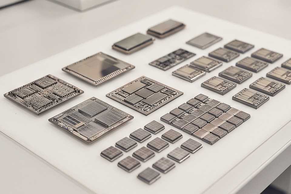
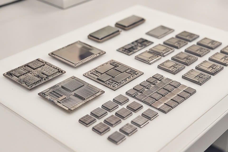
    Semiconductor package samples arranged in various sizes and shapes

    In the semiconductor industry, ‘packaging’ was long regarded as a finishing step placed behind design and process work. However, as demand for AI accelerators and high-performance memory has surged, the situation has changed rapidly. Product competitiveness now depends not only on the performance of a single chip, but on how precisely multiple chips are stacked and connected. Packaging technology now stands at the center of a technology race as intense as semiconductor design itself.
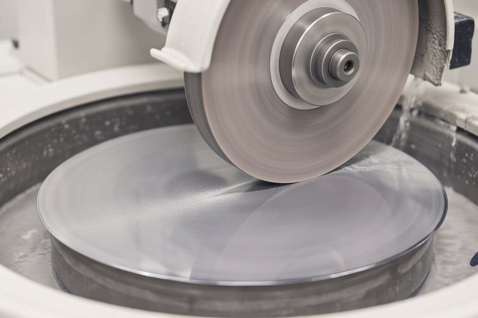
    A diamond wheel uniformly grinding the surface of a semiconductor wafer

    Why Ultra-Precision Grinding Determines Yield

    High-bandwidth memory used in AI accelerators must process more than 1TB of data per second through a vertically stacked structure. To meet this requirement, each stacked chip must have uniform thickness, and surface flatness must also be controlled at the micron level. According to Mordor Intelligence, 3D stacked memory accounts for 34.28% of revenue share in the advanced semiconductor packaging market as of 2025, establishing itself as the leading technology.

    As package formats diversify, such as FCBGA, WLCSP, and QFN, thickness precision standards also vary by type. For example, WLCSP requires a fine pitch between 0.3mm and 0.5mm. Ultimately, grinding precision in the packaging process is a key variable that determines yield. Even a slight increase in thickness variation can undermine the electrical reliability of the entire stacked structure, directly leading to performance degradation in the final product.

    Huvics PKG Grinder responds to these standards with micron-level grinding using a diamond wheel. It is available in both Full Auto and Manual configurations, allowing flexible application according to the production line structure of each customer, while maintaining stable quality even in high-speed processes to achieve high yield. Machining precision is product reliability is the principle that most clearly explains the role this equipment plays in semiconductor packaging processes.
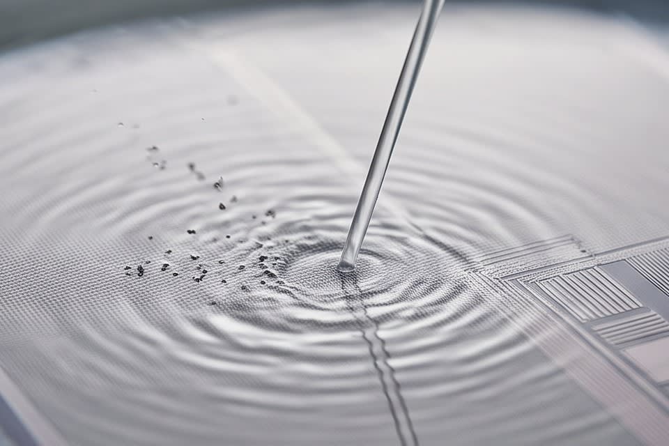
    A cleaning process that sprays liquid onto a semiconductor surface to remove contaminant particles

    Why the Cleaning Process Is the Starting Point of Quality

    If grinding determines the form of packaging, cleaning is the process that ensures this form can perform its intended function. A single fine particle remaining on the semiconductor surface can contaminate the entire subsequent process or lead to defects in the final product. Especially in components that require optical precision, such as camera modules or autonomous driving sensors, invisible contamination can quietly erode product reliability. This is why the cleaning process must be treated not as simple washing, but as the starting point of quality stability.

    Huvics Cleaner System removes contaminant particles from product surfaces by sequentially combining Micro Bubble, Water Jet, and Air Knife, and consistently handles the drying process through its Oven Dry function. Cleaning conditions can be configured differently according to product types such as camera modules, sensors, VCM motors, and trays, enabling a single system to address diverse process requirements.

    In practice, many cases have shown that defects occurring in semiconductor tape bonding processes and yield loss in camera modules can be resolved by improving the cleaning process. Reducing particles reduces defects, and reducing defects increases yield. Engineers who have worked with cleaning processes know well how difficult it is to implement this simple connection in the field. The significance of precision cleaning is confirmed by the fact that it is not the end of the process, but the foundation of quality.
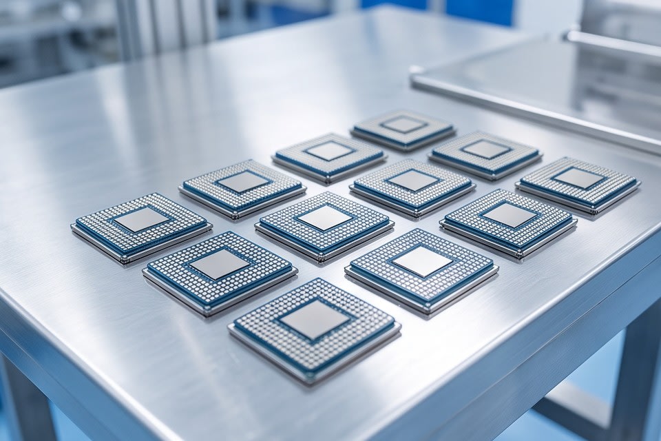
    Precisely processed semiconductor packages arranged in a row

    The competition in semiconductor packaging technology is now shifting toward process precision as much as chip design. Grinding and cleaning are the two pillars that support yield and reliability in this competition. If either one becomes unstable, even the most sophisticated package design will struggle to deliver its intended performance in the field. In an era when technological precision becomes product competitiveness, how firmly each and every process is built will ultimately determine a company’s position in the future semiconductor market.


    Huvics is an advanced technology company that develops and manufactures automation equipment and
    production systems across the semiconductor, LED, Mobile, and Cosmetic industries.
    With top talent and continuous technological innovation, we support customers in improving productivity and
    securing quality competitiveness.

    Huvics Contact

    Tel: 031-374-8285
    Email: cdpark@huvics.com

    Contact Huvics

  • Huvics Technology and Global Partnership Strategy Driving Innovation in the Semiconductor Cleaning Process

    Huvics Technology and Global Partnership Strategy Driving Innovation in the Semiconductor Cleaning Process

    Huvics

    As semiconductor processes enter ultrafine areas measured in nanometers, even the smallest particle on a wafer has become a decisive factor that determines overall production efficiency. Cleaning processes have now moved beyond a simple supporting step to become a core competitive strength that completes semiconductor quality, while requirements on production sites are becoming more complex and demanding every day. Let us explore the innovation journey of Huvics, which overcomes technical challenges in these extreme production environments and presents global standards.

    Global technology and status of Huvics

    Core Value and Technological Leap of the Semiconductor Cleaning Process

    The Importance of Precision Cleaning and the Role of Huvics

    As semiconductor manufacturing technology advances into fine processes, even a small contaminant on the wafer surface can determine the overall yield. In this environment, precision cleaning has established itself as a core stage that determines semiconductor quality and performance. Huvics goes beyond being a simple equipment supplier by providing innovative cleaning solutions that transform the industrial paradigm, strengthening its position in the global market.

    Technological Validation in the Global Market

    In particular, the One Million Dollar Export Tower awarded on Trade Day in 2025 shows that the unrivaled technology of Huvics has been fully proven on the world stage. Based on an extensive patent portfolio accumulated over many years, we are building technical trust by clearly solving the challenges faced by customer companies, even in the most complex semiconductor production environments.

    Sustainable Growth Through Research and Development

    Continuous investment in research and development is the driving force that enables Huvics to maintain its technological advantage in precision cleaning and automation equipment. We deeply understand the importance of the cleaning process, the heart of the semiconductor industry, and have grown into a partner that creates value beyond technology and drives the success of customer companies.

    When we sit with customer companies, listen to their manufacturing process concerns, and propose sophisticated customized equipment, we take pride in building a path toward sustainable growth together beyond simply providing technical answers. As semiconductor processes continue to advance, the innovation brought by Huvics will become even deeper.

    Nano-scale precision cleaning technology

    The Irreplaceable Competitiveness Unique to Huvics

    Site-Focused Customized Solutions

    The growth that Huvics has achieved in the global market is the result of intense problem solving and persistent research and development. The market for precision cleaning and automation equipment in advanced industries is a demanding world that allows no errors, yet we challenge new technical limits every day. In particular, close collaboration with global semiconductor leaders has enabled us to understand the demanding requirements of production sites in real time. The irreplaceable competitiveness unique to Huvics is as follows.

    • Solving individual and complex site problems faced by customer companies beyond standardized equipment
    • Maximizing production efficiency for customer companies by implementing fully optimized customized equipment

    Engineer Commitment and Technical Processes

    The persistence our engineers demonstrate when facing technical challenges comes from a sense of mission to raise process precision to the next level. We believe true partnership is completed only when the production efficiency decline or defect rate issues experienced by customer companies are solved through the equipment we develop.

    The reason Huvics has become recognized as a key partner within the global semiconductor ecosystem is that we have a systematic process for solving technical problems. We do not settle for the present, and we take the lead in directly designing standards for sophisticated cleaning processes. These efforts will become the foundation for establishing technical standards in the global semiconductor industry.

    An Innovation Partner Leading the Future Semiconductor Industry

    Advancement of Precision Cleaning Technology and Future Vision

    Huvics is not satisfied with current success and is concentrating all capabilities on presenting a new direction for future cleaning processes. The advancement of precision cleaning technology contributes to improving efficiency across the industry by maximizing semiconductor yield. We respond one step ahead to rapidly changing market demands and support customer companies in building future-oriented production environments based on our unrivaled technology.

    Technological Pride and Leadership in Global Standards

    We are confident that the sophistication of the technology we design will dramatically improve the efficiency of semiconductor processes and become an important catalyst for opening the next-generation semiconductor world. Our journey to elevate the status of the Korean semiconductor equipment industry on the global stage is rooted in corporate pride to change the world for the better through technology.

    The value we create in the core field of cleaning processes strengthens trust across the semiconductor industry and becomes a driving force that expands possibilities beyond the limits of technology. Huvics will continue to lead global standards based on its unique philosophy and research capabilities, and will never stop its role as an innovation partner that makes the heart of the semiconductor industry beat stronger.

    Efficiency of automated process systems

    Manufacturing Environments Completed with Integrated Solutions

    Rapid Change and Unrivaled Patented Technology

    Semiconductor manufacturing processes require greater technical precision and speed than ever before, and amid this rapid change, Huvics always considers solutions that stay one step ahead. As technology becomes more complex, cleaning processes require higher levels of automation and precision control, and Huvics is overcoming these challenges head on based on its accumulated and unrivaled patented technologies.

    Optimization of Customer Company Production Environments

    Beyond simply making excellent equipment, the process of deriving the optimal solution from an integrated perspective that covers the entire process line of customer companies is deeply embedded in the DNA of our organization. The One Million Dollar Export Tower award in 2025 is only the result of such efforts, and our journey is now moving toward even greater global standards.

    What we create is not merely equipment composed of metal and control devices, but the complete manufacturing environment envisioned by customer companies. Analyzing the complex variables of semiconductor production sites and optimizing them with our own cleaning technology is demanding work, but the resulting yield improvement and process stability deliver an irreplaceable sense of achievement.

    Huvics will continue to become the most powerful partner trusted by the global semiconductor market through sincere passion for technology and continuous investment in research and development. As we design the future of sophisticated cleaning processes and as that future becomes reality, Huvics will be there, remaining a source of technological pride for the global semiconductor industry.

    Future vision of smart factories

    Closing Remarks

    Ultimately, the success of the semiconductor industry is determined by the precision cleaning performed on site, in other words, by perfection at the smallest scale. As proven by the One Million Dollar Export Tower award, Huvics has become an irreplaceable partner trusted by the global semiconductor ecosystem through persistent research and innovation that turn technical challenges into opportunities.

    Beyond simply supplying equipment, our steps to optimize the production environments of customer companies represent a journey of writing new standards for the Korean semiconductor equipment industry. Huvics will continue to expand the limits of technology based on sophisticated technical capabilities and a strong sense of mission so that the heart of the semiconductor industry can beat even stronger.


    Huvics is an advanced technology company that develops and manufactures automation equipment and
    production systems across the semiconductor, LED, Mobile, and Cosmetic industries.
    With top talent and continuous technological innovation, we support customer productivity improvement and
    quality competitiveness.

    Huvics Contact Information

    Phone: 031-374-8285
    Email: cdpark@huvics.com

    Huvics Inquiry