

Semiconductor quality management is, in simple terms, a matter of how precisely allowable tolerances are controlled at each stage of the process. Invisible micron-level variations determine the reliability of the finished product, and this issue becomes even more apparent in advanced package structures where chips are stacked in multiple layers. The moment terms such as ‘thickness uniformity’ or ‘flatness’ come up on the manufacturing floor, they are not simply about dimensions but about issues that affect overall yield and reliability.
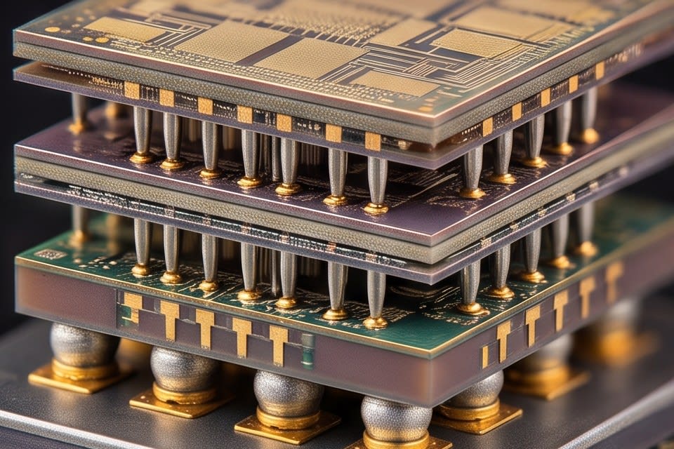
Why Thickness Variation Undermines Package Reliability
Stacking chips also means, in a sense, stacking tolerances. In structures such as AI semiconductors or high-performance memory, where dozens of dies are vertically stacked, thickness variation in each layer accumulates and compromises the flatness of the entire package.
The international semiconductor standard JEDEC defines the maximum allowable warpage for large flip chip packages as 200μm, and cases have been reported where warpage deformation reaches 87μm under reflow temperature conditions. Once this value exceeds the threshold, signal integrity becomes unstable and interlayer bonding defects can occur.
In high-bandwidth memory, it is already widely recognized across the industry that thickness variation alone in the interposer manufacturing process can cause impedance deviation. If thickness is not uniform, electrical performance cannot be uniform either, and the principle that an uneven package cannot be reliable has become the starting point of advanced package design.
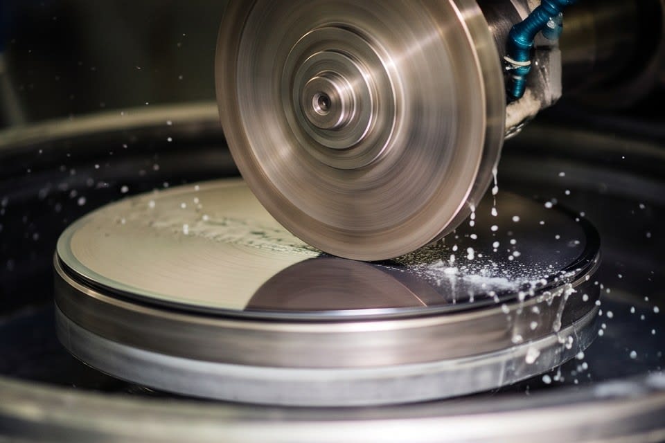
How a Reference Surface Is Created in the Grinding Process
PKG Grinder is equipment that directly addresses this issue. Regardless of package type, including FCBGA, WLCSP, QFN, DFN, and Solar Cell, it performs micron-level precision grinding to achieve the target thickness required by the customer.
This machining method, implemented through the combination of a high-precision stage and a diamond wheel, maintains uniform results even in high-speed processes without reducing yield, contrary to the common belief that speed and precision are usually inversely related. Because it supports both Full Auto and Manual configurations, it can respond flexibly to everything from low-volume, high-mix lines to mass production systems.
Grinding is not simply a task of reducing thickness. It is the process of creating a reference surface on which all subsequent processes depend. Since the uniformity and flatness of that reference surface determine the reliability of the final package, precision control in the grinding stage is the practical key to securing quality.
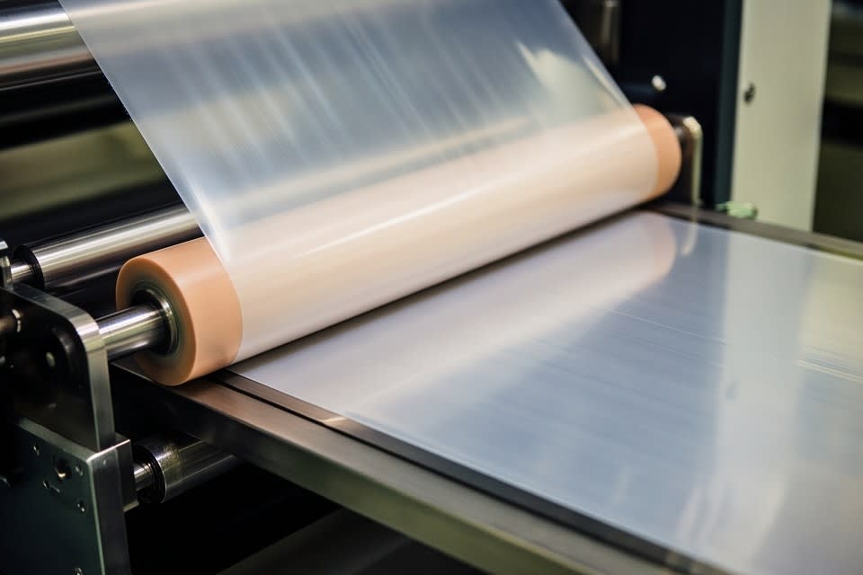
The Impact of the Lamination Process on Adhesion Reliability
Thickness uniformity issues do not occur only in the grinding process. If film thickness is formed unevenly during the ABF lamination process, the electrical performance of subsequent circuits varies from layer to layer and reliability decreases.
Lamination may appear to be a simple process of attaching film, but even a slight imbalance in the combination of temperature and pressure can cause delamination defects or uneven adhesion strength. According to research findings, cases have been reported where delamination defects decreased by up to 67% when optimized lamination parameters were applied.
Huvics’ laminator system features an integrated process structure that connects everything from Expander to UV Curing in a single flow, and secures both adhesion strength and process stability through Lamp and LED type UV curing systems. With Semi Auto and Manual options, it can support various product specifications and production requirements, and it is designed to reduce takt time by simplifying process steps.
Field applications continue to confirm that overall package quality stability is achieved only when the two processes, setting the reference surface through grinding and building layers through lamination, are each precisely controlled.
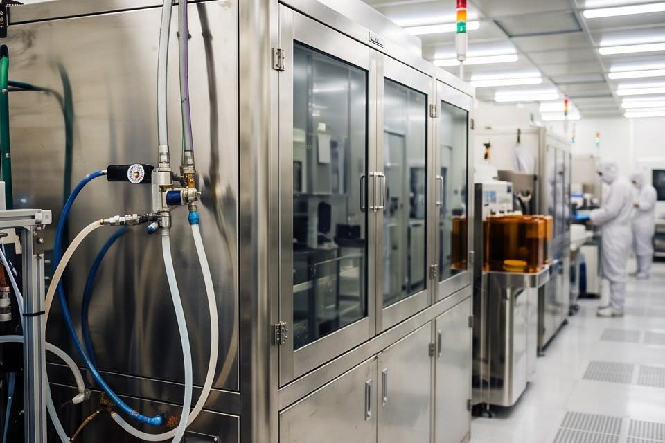
Semiconductor package quality cannot be guaranteed by the completeness of a single process alone. Reliable results emerge only when the uniform reference surface created in the grinding stage works together with precise temperature and pressure control in the lamination stage. Managing micron-level variation is ultimately a matter of designing the entire process as one connected flow, and the essence of quality management lies in how tightly the allowable tolerance of each stage can be narrowed within that flow.
Huvics is an advanced technology company that develops and manufactures automation equipment and
production systems across the semiconductor, LED, Mobile, and Cosmetic industries.
With top talent and continuous technological innovation, we support customers in improving productivity and
securing quality competitiveness.
Huvics Contact
Phone: 031-374-8285
Email: cdpark@huvics.com
