Tag: vision inspection

  • When 1 Micron Determines Yield in the Field: Key Insights into the Chip Stacking Grinding Process

    When 1 Micron Determines Yield in the Field: Key Insights into the Chip Stacking Grinding Process

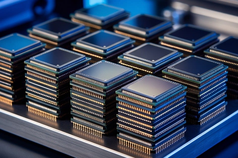
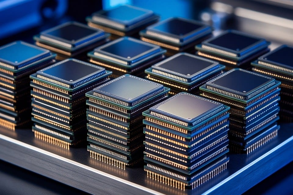
    Semiconductor chips neatly aligned and vertically stacked.

    There is a joke often shared among semiconductor design engineers. “The more chips you stack, the better, but the problem is that stacking them is far too difficult.” In real packaging processes where dozens of chip layers are stacked, the first thing to fail is not the design drawing, but flatness. In a world where a 1 micron difference can disrupt overall yield, the meaning of “grinding well” carries far more weight than expected.
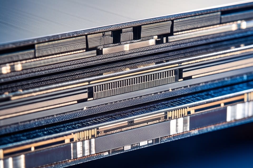
    A cross section of semiconductor chips precisely stacked with microscopic spacing.

    Why TTV Matters in Chip Stacking Structures

    In structures where chips are stacked in multiple layers, thickness variation in each layer is not just a dimensional issue. As layers accumulate, microscopic errors build up and eventually lead to electrical bonding defects or concentrated structural stress. The metric used to express this numerically is total thickness variation, or TTV.

    The TTV required in chip stacking structures is at the level of 1 micron or less, demanding precision far below one hundredth of the thickness of a human hair. If this standard is not met, bonding surfaces can lift during subsequent bonding processes or heat dissipation can become uneven, undermining the reliability of the device itself. For products such as AI semiconductors or high performance memory that vertically connect dozens of chips, the allowable variation range becomes even narrower.

    One reason TTV control is difficult in the field is the structural variables of the grinding equipment itself. The wear pattern of the grinding wheel, microscopic vibration generated during spindle rotation, and changes in the flatness of the chuck that fixes the wafer act together to make the thickness profile uneven. Uniform flatness cannot be achieved simply by turning on the equipment. How precisely these variables are controlled is the key factor that determines the yield of the entire packaging process.
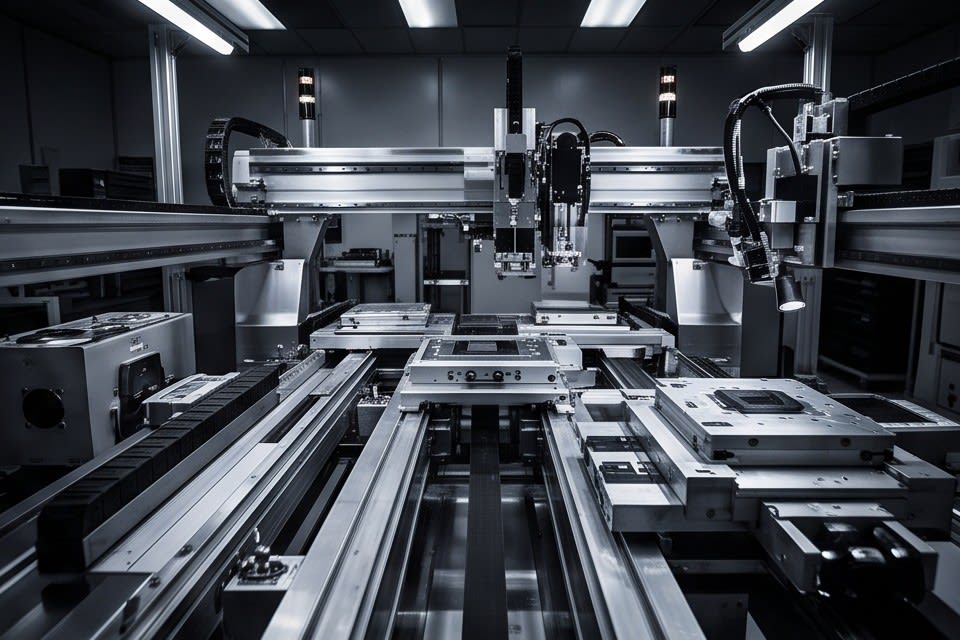
    Semiconductor process equipment equipped with a high precision stage and grinding head.

    Ultra Precision Grinding Design of the PKG Grinder

    There is a way to address this issue from the process equipment design stage. The PKG Grinder from Huvics combines a high precision stage with a diamond wheel to process various package types such as FCBGA, WLCSP, and QFN/DFN at micron level accuracy. The key is a control structure that keeps TTV variation within a defined range even during high speed processing. The TTV requirement for ultra thin wafer stacking processes is approximately 2.0 microns or less, and to meet this value reliably in a high speed grinding environment, spindle runout compensation and chuck flatness maintenance must be built into the equipment from the design stage.

    Another practical challenge in production sites is line flexibility. In many cases, the same equipment must handle both low volume high mix processes and high volume continuous production. The option to choose Full Auto A·B types or a Manual type is a design choice made to respond to this requirement, and it directly contributes to reducing setup loss during process changeovers. Speed and uniformity are usually in conflict, but in grinding equipment, they are implemented in a way that satisfies both conditions at the same time.
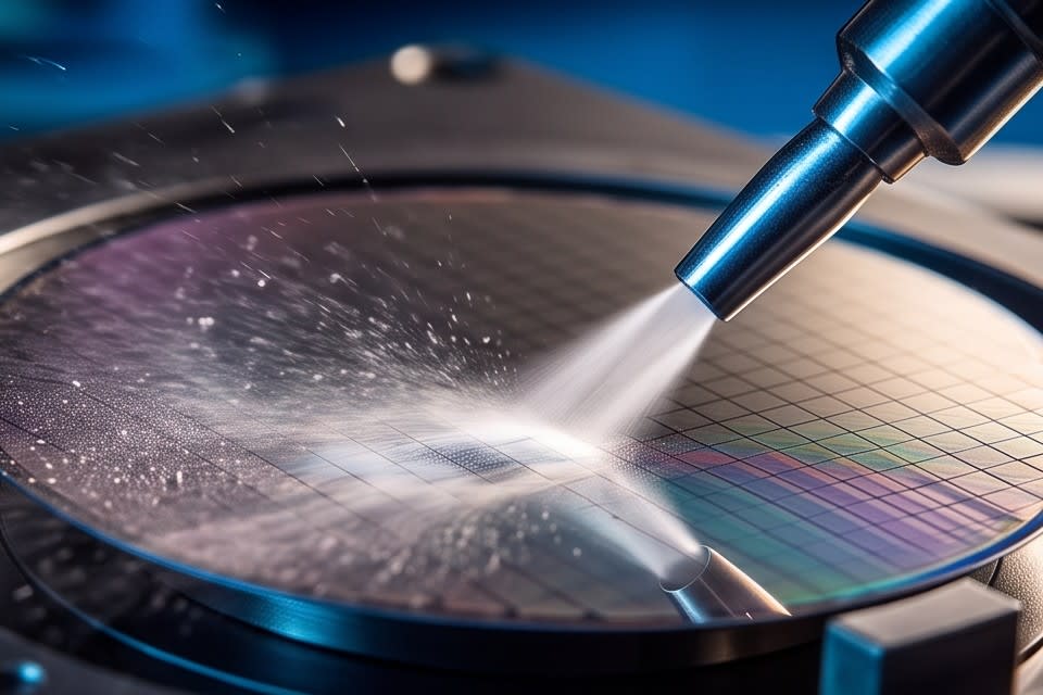
    Cleaning and drying process that removes surface residue after grinding.

    The Role of Cleaning and Drying After Grinding

    Flatness control does not end just because the grinding process is complete. Immediately after machining, grinding residue and fine particles remain on the wafer surface, and the way they are removed determines the final surface quality. This is where the choice of cleaning and drying methods becomes important.

    Comparison of Air Knife and IPA Vapor Drying

    The two drying methods mainly used in the industry are Air Knife and IPA vapor drying. Air Knife mechanically pushes liquid off the surface using a high speed gas jet, and according to research published on ResearchGate, drying within 2 seconds is possible under a speed condition of 150mm/s. In contrast, IPA vapor drying uses ultrapure isopropyl alcohol vapor to lower surface tension and guide moisture to flow away naturally without leaving marks.

    Because the two methods control processing speed and the risk of surface residue in different ways, the selection criteria vary depending on the surface characteristics of the target device and the process requirements.

    Multi Step Cleaning for Components Sensitive to Surface Contamination

    For components sensitive to surface contamination, such as camera modules, sensors, and VCM motors, a multi step cleaning approach that combines micro bubbles and water jets is becoming established.
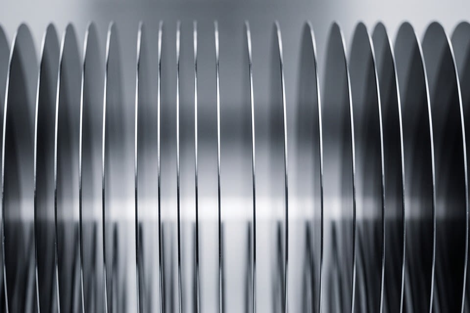
    A circular plate structure expressing the precision of the semiconductor chip stacking process.

    More than how many chips are stacked, how uniformly they are stacked determines the actual yield. From grinding precision to the selection of cleaning and drying methods, the quality of the packaging process is completed on a structure where each stage supports the next. The joke mentioned at the beginning, “stacking them is far too difficult,” turns out to describe the essence of process design quite accurately.


    Huvics is an advanced technology company that develops and manufactures automation equipment and
    production systems across the semiconductor, LED, Mobile, and Cosmetic industries.
    With top tier talent and continuous technological innovation, we support improvements in customer productivity and
    help secure quality competitiveness.

    Huvics Contact

    Phone: 031-374-8285
    Email: cdpark@huvics.com

    Contact Huvics

  • 3 Key Process Points to Reduce Defect Rates in Semiconductor Cleaning and Processing

    3 Key Process Points to Reduce Defect Rates in Semiconductor Cleaning and Processing

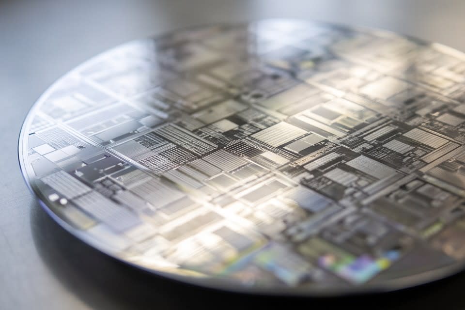
    Semiconductor wafer densely patterned with microscopic circuit lines

    As the linewidths of circuits etched onto a single semiconductor chip have narrowed to the scale of just a few nanometers, the limits of acceptable contamination in the manufacturing process have also changed. In the past, it was enough to filter out foreign matter that was difficult to detect with the naked eye. Today, even a single fine particle floating in the air can become a variable that damages an entire circuit. As processes become more precise, the standards required of cleaning equipment have risen as well, and cleaning has become a core process that determines yield, not a final step for checking quality.

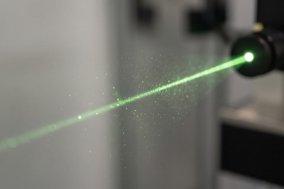
    Airborne fine particles visualized and floating in laser light

    The structure in which particle contamination determines yield

    In semiconductor processes, the impact of particle contamination on yield increases sharply as process generations advance. According to Applied Physics USA, in sub-10nm processes, aerosols measuring 0.1 to 0.5 micrometers are considered among the greatest risk factors, and even a single 10nm particle can cause a short circuit or structural deformation in a transistor.

    The reality that even within the same production line, yield can vary between 95% and 75% depending on the level of particle contamination control shows that the cleaning process is not simply a matter of hygiene. As miniaturization progresses, the tolerance for contamination becomes narrower, and how precisely foreign matter is removed in the early stages of the process effectively determines the quality of the final product. This is why cleaning equipment is no longer a lower priority in process design, but has moved to the center of yield strategy.

    As particle size becomes smaller, the precision required to detect and remove those particles also increases. Process miniaturization is changing the very criteria used to select equipment.

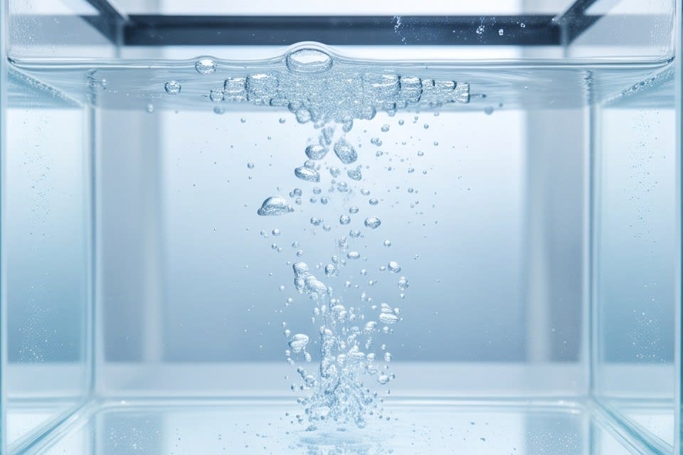
    Dynamic bubbles formed as water droplets fall

    Principles and field application of multi stage cleaning technology

    The performance of cleaning equipment depends on how contamination particles are separated from the surface. Micro bubble cleaning removes particles with shock waves generated when bubbles tens of micrometers in size collapse near the surface. In a study published in the Korean Journal of Chemical Engineering, a maximum jet flow velocity of 148.5mm/s was confirmed in a micro cylinder array structure, and this level of flow velocity is effective for removing fine contaminants with strong surface adhesion.

    Nanobubble technology uses bubbles smaller than 5nm to reach even finer particles, and because the bubbles remain stable for a long time, cleaning efficiency is maintained even on complex surface structures.

    Engineers handling components with different shapes in the field, such as camera modules, sensors, VCM motors, and trays, understand that it is difficult to process every product with a single method. This is why multi stage cleaning structures that combine Micro Bubble, Water Jet, and Air Knife are chosen for actual production lines.

    The drying process, which completely removes residual moisture after cleaning, must also be integrated into a single flow to reduce the risk of foreign matter reattaching between processes. Designing cleaning and drying as one continuous system has become essential for securing quality stability.

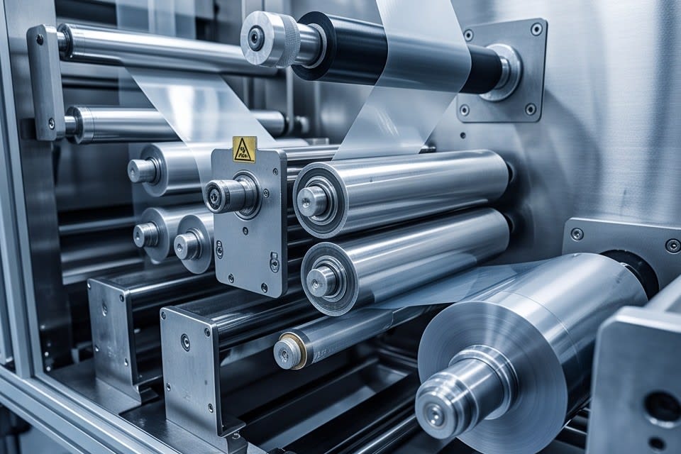
    Drive unit of lamination equipment where tape is supplied through rollers

    Thickness uniformity and process integration determine defect rates

    To reduce defects in the package processing stage, the first requirement is to clearly define the criteria for selecting equipment. The allowable range of total thickness variation, TTV, required in high performance packaging is typically 0.5 to 2.0 micrometers, and this standard becomes even stricter for products that stack chips in multiple layers, such as AI semiconductors and high performance memory.

    Huvics takes an approach that structurally reduces defect factors occurring after cleaning through its PKG Grinder and Laminator System. The PKG Grinder uses a high precision stage and diamond wheel to uniformly process various packages, including FCBGA, WLCSP, QFN, and DFN, at the micron level, and its core role is to keep thickness variation within the allowable range. The Laminator System handles tape attachment and curing processes from Expander to UV Curing within a single line, reducing contamination and alignment errors that can occur during movement between processes.

    Cases in which defects in semiconductor tape bonding processes or foreign matter issues in camera modules were resolved through cleaning and integrated process design show that equipment selection goes beyond simply comparing specifications. As stacking becomes deeper and package structures become more complex, thickness uniformity and process continuity act as the criteria that determine defect rates. The answer to what it means for final yield to reduce variables at a specific process stage is already embedded in the equipment design.

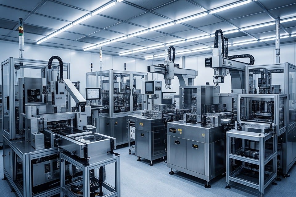
    Precision automation equipment organically arranged at a semiconductor production site

    As semiconductor processes become more precise, the role of cleaning and processing equipment is shifting from simple support to the center of yield management. In an environment where the size of a single contamination particle can affect overall yield, the principle used to remove particles and the method used to control thickness variation become the practical standards for equipment selection. As the pace of process miniaturization accelerates, the importance of equipment that meets these standards will continue to grow.


    Huvics is an advanced technology company that develops and manufactures automation equipment and
    production systems across the semiconductor, LED, Mobile, and Cosmetic industries.
    With top talent and continuous technological innovation, Huvics supports customers in improving productivity and
    securing quality competitiveness.

    Huvics Contact

    Phone: 031-374-8285
    Email: cdpark@huvics.com
    Huvics Inquiry

  • Manual Inspection vs Automated Cleaning and Drying System, Where Semiconductor Yield Is Decided

    Manual Inspection vs Automated Cleaning and Drying System, Where Semiconductor Yield Is Decided

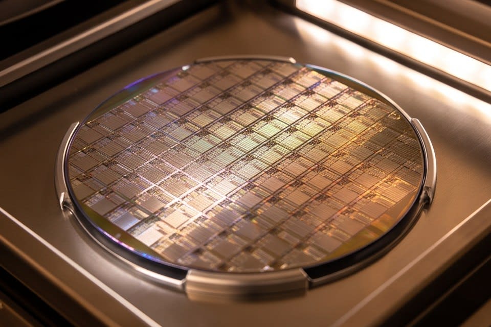
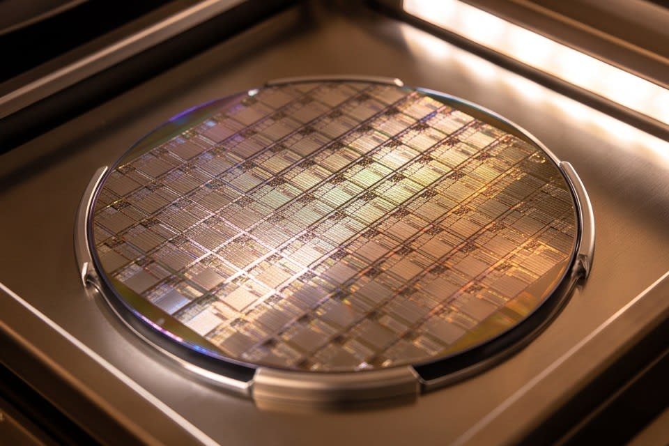
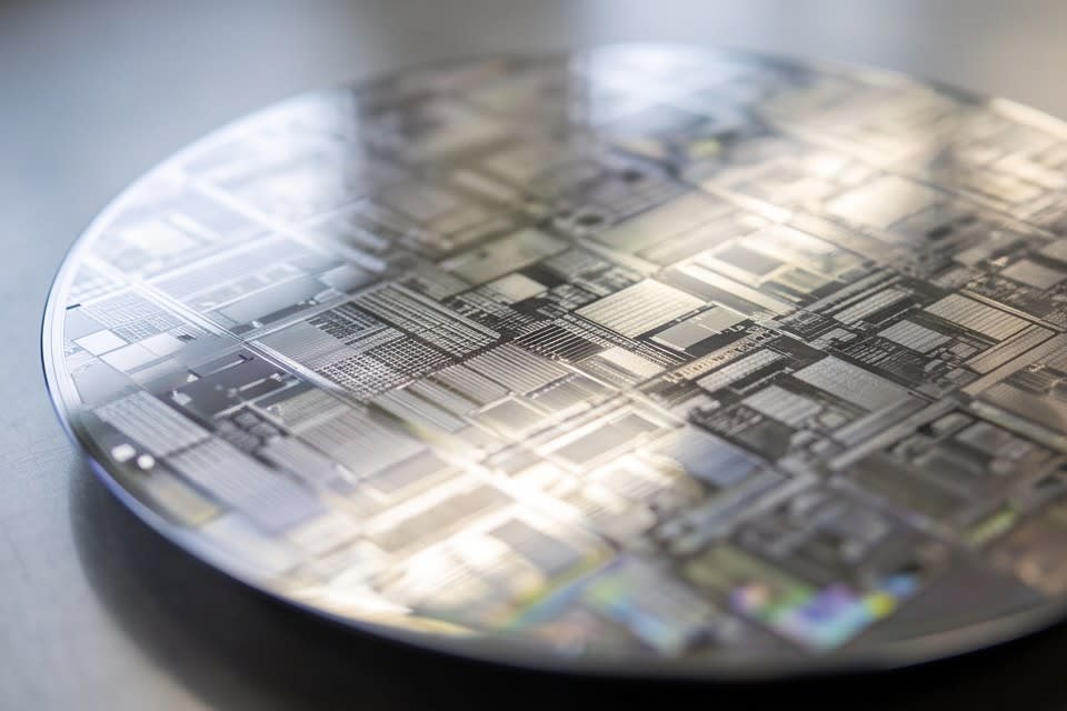
    Precisely integrated circuit patterns on a semiconductor wafer.

    There is a saying among semiconductor process engineers. “If you take cleaning lightly, you can easily lose yield.” Of course, it is hard to confirm whether anyone actually says this, but that is exactly the atmosphere on the production floor. A single speck of dust or one drop of oil can bring down an entire process that has been built with extreme precision. Cleaning may look like the final step of a process, but in reality, it is the starting line of quality.

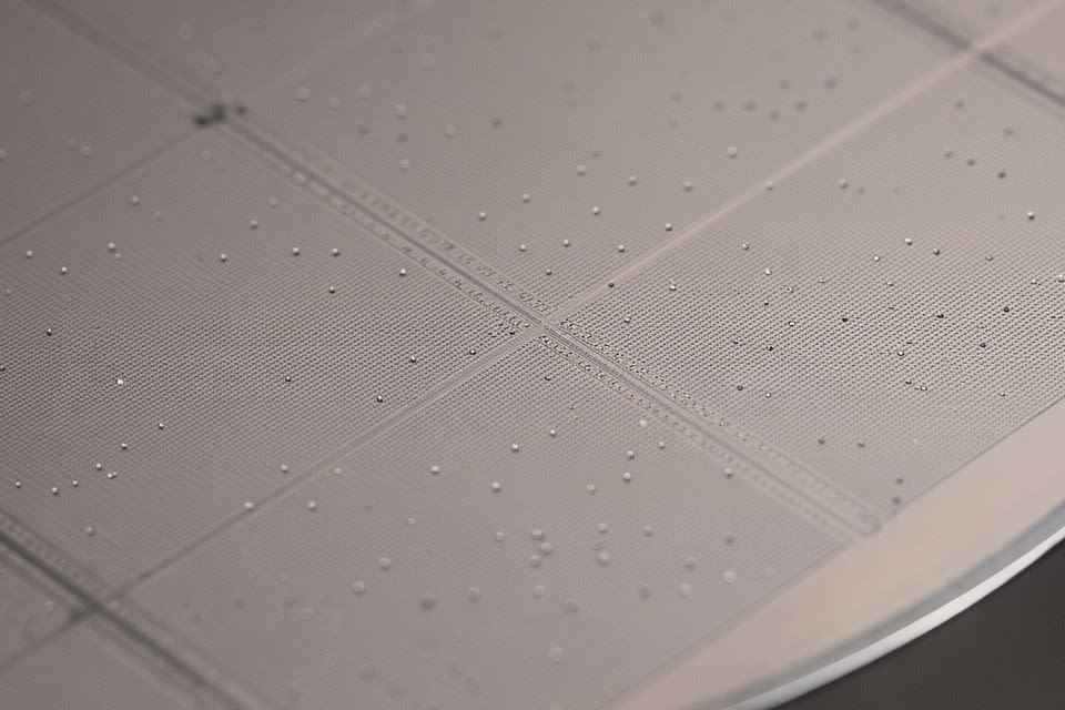
    A close up view of microscopic particles scattered across the surface of a semiconductor wafer.

    The Impact of Microscopic Contamination Particles on Yield

    In semiconductor and advanced electronic component manufacturing, microscopic contamination particles are not simple impurities. According to analysis by TSI, a single particle on a wafer can lead to failures in multiple integrated circuits and significantly reduce overall yield. What makes the issue even more demanding is size. The fact that particles as small as 0.05 micrometers can cause critical defects in semiconductor chips clearly shows that the cleaning process is not just a simple act of washing.

    It is already widely recognized in the industry that particle defects account for a significant share of all defects in high density electronics manufacturing. As ultra fine processes become standard, contamination tolerance limits become even tighter, and the technical completeness of the cleaning stage is increasingly determining the reliability of the final product.

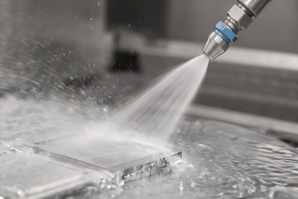
    A high pressure stream of water sprayed from a nozzle washing the surface of a component.

    Multi Stage Cleaning and Drying Technology of the Cleaner System

    The Cleaner System approaches this problem step by step. Its configuration, consisting of Micro Bubble, Water Jet, Air Knife, and Oven Dry, allows each stage to remove contamination and complete drying in a different way.

    Micro bubbles are fine bubbles with diameters ranging from 10 micrometers to several tens of micrometers. They are generated when dissolved air reaches a certain concentration and physically separate contamination particles adhered to the surface. Water Jet removes surface residues with a high pressure water flow, while Air Knife pushes away moisture with a sharp air stream to create the proper condition for the next stage. The final Oven Dry stage completely removes remaining moisture and completes the drying process.

    Depending on the product type, such as camera modules, sensors, VCM motors, and trays, a Full Auto or Manual configuration can be selected to match the conditions of the production site. It is implemented through a design method that treats cleaning and drying not as separate processes, but as one continuous flow.

    Combining Vision Inspection and Ultrasonic Dispersion Technology

    Precision is also required without compromise in the quality verification stage after cleaning. While manual inspection, even when performed by skilled operators, remains at an accuracy level of 85~90%, research published on ResearchGate shows that automated optical inspection(AOI) achieves 98~99% accuracy and processing efficiency of more than 5,000 units per hour. At the point where the human eye reaches the limits of fatigue and concentration, algorithms operate without fluctuation.

    Huvics applies this principle to MLCC and FPCB processes by combining its proprietary ultrasonic dispersion technology with vision inspection algorithms. Ultrasonic dispersion increases particle separation efficiency during the cleaning stage, and the vision inspection algorithm detects remaining defects down to a microscopic level afterward. Because the two technologies operate sequentially, the performance of one stage supports the effectiveness of the other. The key is to connect the cleaning process and the inspection process within a single quality management system, rather than treating them separately.

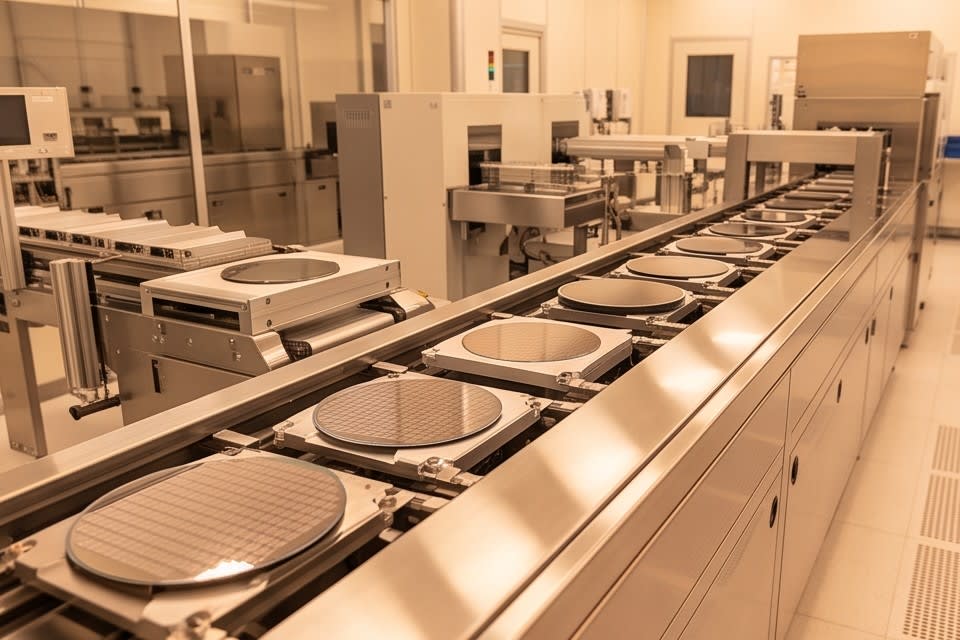
    Multiple wafers moving along automated equipment.

    There is something often overlooked when selecting a cleaning and drying system. It is not just the performance of the equipment, but how it connects with the entire process. No matter how precise the cleaning technology is, if it does not align with the inspection stage, defects are found too late and yield loss has already accumulated. In semiconductor and advanced component manufacturing, quality stability is not created by the completeness of a single process, but by the entire flow from cleaning to drying and inspection. How that flow is designed ultimately determines product reliability.


    Huvics is an advanced technology company that develops and manufactures automation equipment and
    production systems across the semiconductor, LED, Mobile, and Cosmetic industries.
    With top talent and continuous technological innovation, Huvics supports customers in improving productivity and
    securing quality competitiveness.

    Huvics Contact

    Phone: 031-374-8285
    Email: cdpark@huvics.com
    Huvics Inquiry

  • Are you applying dispersion, inspection, and integration step by step in your semiconductor cleaning process?

    Are you applying dispersion, inspection, and integration step by step in your semiconductor cleaning process?

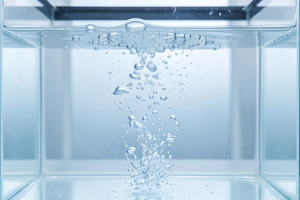
    Fine bubbles rising in liquid

    According to a study published in the Korean Journal of Chemical Engineering in 2022, acoustic vibration generated in microbubble arrays creates jet flow velocities of up to 148.5mm/s and removes particles from semiconductor surfaces with 92.5% efficiency. This figure shows that cleaning is not simply a sanitation process, but a key variable that determines semiconductor reliability. As package structures become more complex, the required precision of cleaning technology is also increasing, and within this trend, which technologies create a real difference has become a central question for the industry.

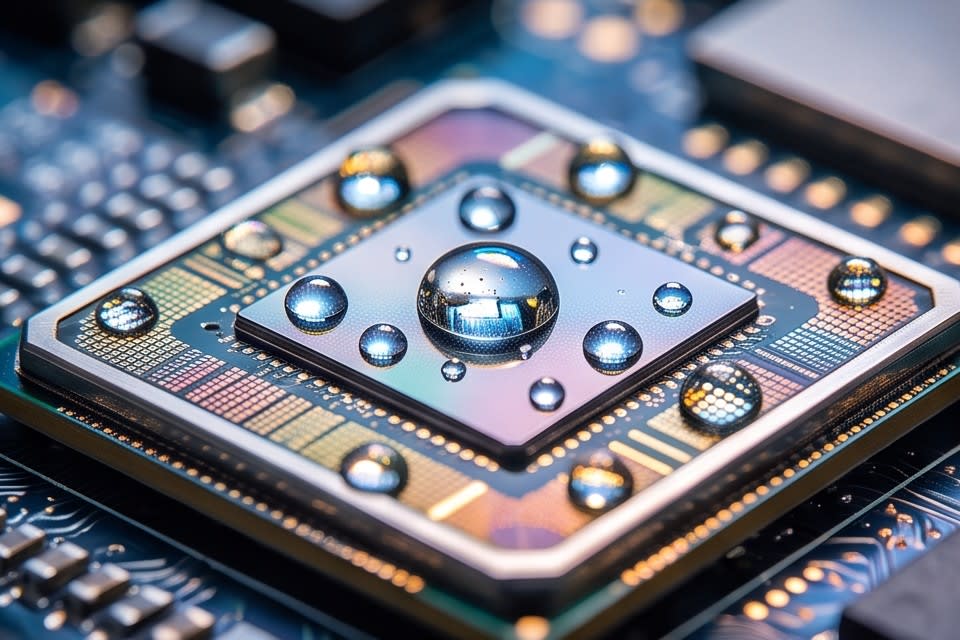
    Small water droplets on the surface of a fine semiconductor package

    Technical demands that fine package structures place on the cleaning process

    As semiconductor packages become more advanced, the technical burden placed on the cleaning process grows rapidly. Packages with fine pitch structures, such as FCBGA and WLCSP, leave flux residues and contaminant particles deep inside narrow capillary-like spaces after solder reflow. If these residues are not completely removed, electrical reliability may be compromised, directly affecting long-term service life.

    The issue is that as structures become more precise, simply increasing cleaning energy can instead raise the risk of structural damage. Without controlling bubble cavitation, it is difficult to strike a balance between cleaning efficiency and structural preservation. Nanobubbles function by increasing heterogeneous nucleation on the surface, reducing adhesion between contaminants and the surface. This principle opens the possibility of removing fine particles without physical impact.

    This is why the direction of cleaning technology is shifting from simple high-power methods to precise physicochemical control. Process results are determined by the mechanism used to separate particles.

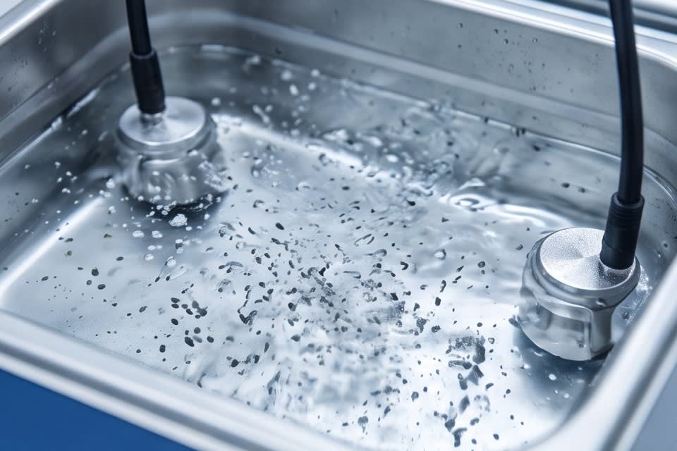
    A vibrating device generating waves in liquid to disperse particles

    Process quality control created by combining ultrasonic dispersion and vision inspection

    The reason ultrasonic dispersion technology is gaining attention in cleaning processes is not simply because it applies vibration energy. The key lies in reducing quality variability across the process by uniformly dispersing material particles in liquid at the micro level. In polishing processes as well, it has been confirmed that achieving uniform particle distribution through ultrasonic dispersion can prevent scratches and defects caused by excessive particles.

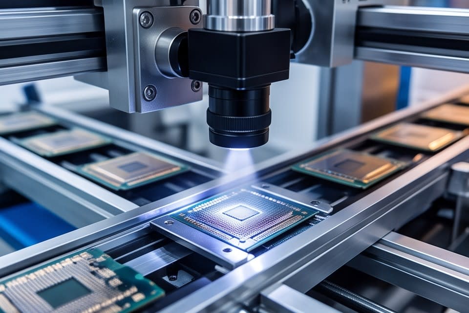
    In highly integrated electronic components such as MLCC and FPCB, this uniformity is directly linked to assembly reliability. If the cleaning solution does not act uniformly, cleaning results vary by component, and that variation leads directly to lower yield. When a vision inspection algorithm is added, defects in fine patterns can be detected in real time, creating a structure that blocks defects before they move on to the next process.

    Unlike when the two technologies operate independently, process feedback speed changes when dispersion control and defect detection occur simultaneously. Process improvement becomes possible only when data can track when and where defects occur. Securing both the uniformity of dispersion and the real-time capability of inspection is the key to cleaning processes for highly integrated components.

    Large-scale automated stainless steel cleaning equipment composed of multiple pipes

    Impact of the Huvics laminator system on production efficiency and yield

    The Huvics laminator system integrates the core lamination processes from Expander to Tape Mounting and UV Curing into a single line. It is structured to reduce transfer errors and waiting time that occur when processes are operated separately, while minimizing quality variation between each stage. Since production time in PCB lamination can vary from several hours to several days depending on optimization, the time-saving effect brought by process integration is difficult to ignore.

    In the cleaning process, a multi-stage method applies Micro Bubble, Water Jet, and Air Knife step by step to remove surface contamination from components with different shapes, including camera modules, sensors, VCM motors, and trays. With a built-in Oven Dry function, the system is designed to complete drying after cleaning on the same line, reducing the risk of contamination reentry that can occur when separate external drying equipment is operated.

    With selectable Lamp and LED UV Curing methods, the system flexibly responds to product groups with different requirements for adhesive strength and process stability. Since both Full Auto and Manual options are available, the same process design can be applied to lines with different production scales or automation levels. In advanced component manufacturing sites, equipment design is moving toward reducing process steps while maintaining the quality standards of each stage.

    A precision vision camera capturing semiconductor components on a conveyor

    As semiconductor packages become thinner and more densely packed, the precision standards required of cleaning processes continue to rise. In a structure where even a single residue left in a fine space can compromise the reliability of an entire component, the principles of cleaning technology and process design are not a matter of choice, but a matter of yield. The reason the market is now paying close attention to semiconductor cleaning technology is that quality stability can only be secured when the uniformity of ultrasonic dispersion, the real-time capability of vision inspection, and the efficiency of process integration work together.


    Huvics is an advanced technology company that develops and manufactures automation equipment and
    production systems across the semiconductor, LED, Mobile, and Cosmetic industries.
    With top talent and continuous technological innovation, we help customers improve productivity and
    secure quality competitiveness.

    Huvics Contact

    Phone: 031-374-8285
    Email: cdpark@huvics.com
    Contact Huvics

  • Huvics Micro Pattern Quality Innovation Strategy Powered by Ultrasonic Dispersion Technology and Intelligent Vision Inspection

    Huvics Micro Pattern Quality Innovation Strategy Powered by Ultrasonic Dispersion Technology and Intelligent Vision Inspection

    Huvics

    In increasingly complex smart devices, even a microscopic contaminant that cannot be seen with the naked eye can disrupt overall yield. This is a challenge that many people on the manufacturing floor have faced at least once. Foreign particles hidden between the micro patterns of highly integrated components are difficult to control completely with conventional cleaning methods alone, making the need for stable quality in production environments even more urgent.

    Huvics precisely identifies these on-site challenges and presents a new solution that combines proprietary ultrasonic dispersion technology with intelligent vision inspection. Let us explore an innovative strategy for minimizing defect rates and maintaining global-level quality even in demanding process environments.

    View of a smart factory

    Key Challenges in Highly Integrated Component Manufacturing and Huvics Ultrasonic Technology

    Microscopic Contaminants and Process Limitations

    In advanced electronic component manufacturing sites, especially in processes that produce highly integrated components such as multilayer ceramic capacitors or flexible circuit boards, microscopic contaminants are more than simple dust to be removed. They are decisive variables directly linked to product performance, because even a single fine particle can determine overall yield.

    The reality is that contamination in these micro patterns encountered on the manufacturing floor is difficult to resolve fundamentally with conventional cleaning methods. To overcome these limitations, Huvics has introduced proprietary ultrasonic dispersion technology into the process and adopted an advanced approach that precisely controls the process environment itself.

    Technical Features of Ultrasonic Dispersion Technology

    The technical features of Huvics are as follows.

    • Uniformly disperses material particles inside liquid at the micro level to prevent quality variation
    • Maximizes cleaning efficiency by optimizing the physical properties of the material itself beyond removing external foreign substances
    • Provides precision control that completely removes even the smallest contaminants remaining between micro patterns

    This precision control capability has become a core driving force that dramatically improves production efficiency on the manufacturing floor, establishing a new standard for high-value-added component manufacturing.

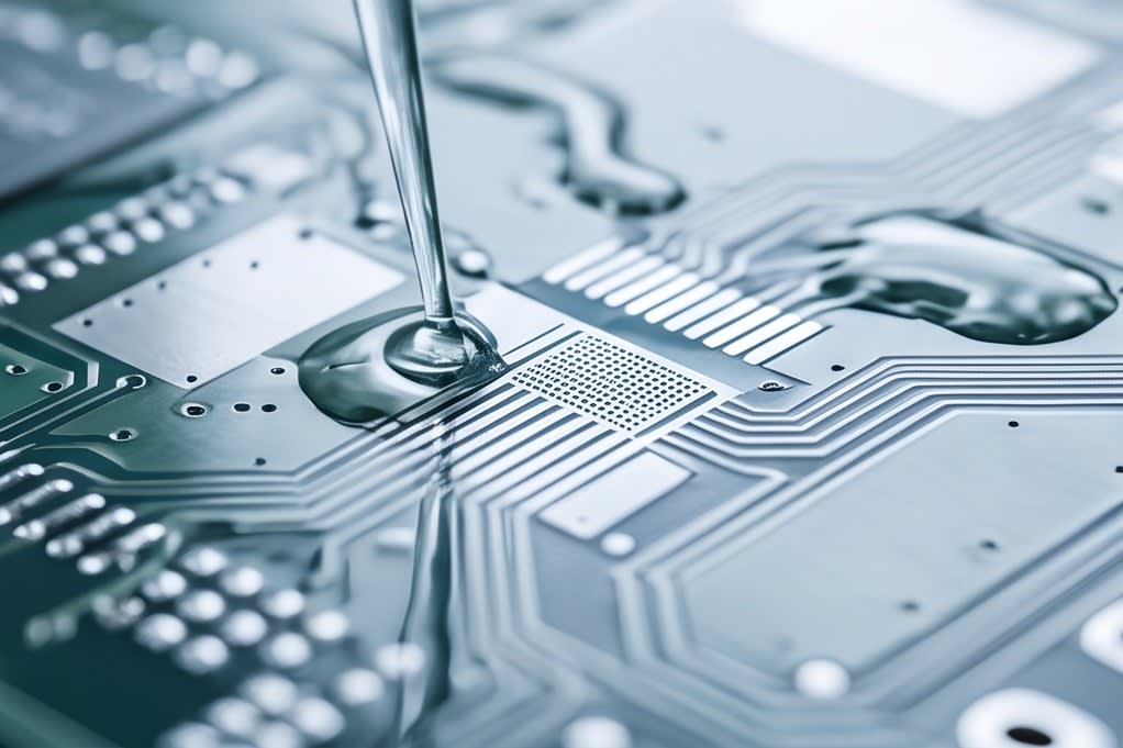
    Precision cleaning of micro pattern circuits

    Completing Quality Control Through Intelligent Systems

    Integration of the Inspection Process After Cleaning

    The technical value provided by Huvics does not stop at the cleaning process that simply washes away contamination. Building an intelligent system that considers the stages after cleaning becomes an important foundation for raising the completeness of quality control to the next level.

    After precisely cleaning micro patterns with its proprietary ultrasonic dispersion technology, Huvics intelligently integrates advanced vision inspection algorithms into the inspection process that immediately follows. This is a sophisticated design intended to instantly identify even the smallest defects in highly integrated components in real time and maximize reliability from the initial assembly stage.

    Solutions for Global Competitiveness

    In a market environment where smart device specifications continue to rise and internal designs become more complex, the biggest concern for manufacturers is how to minimize defect rates and maintain consistent quality even in demanding process environments. The solution from Huvics provides the clearest answer to this challenge.

    • Fully controls process variables through precision cleaning using ultrasound
    • Responds proactively to market changes through real-time monitoring using vision algorithms
    • Supports customers in securing a distinctive technological advantage in global competition

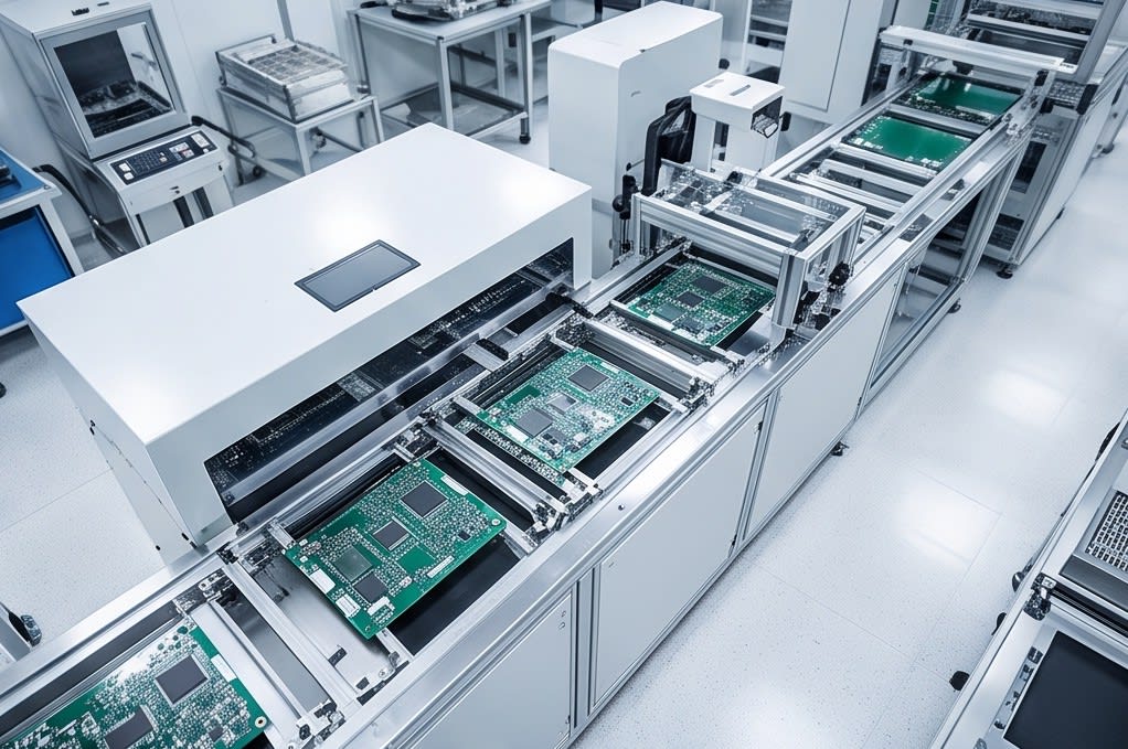
    Automated PCB inspection process

    The Value of Huvics That Defines Manufacturing Competitiveness

    Controlling contamination in micro patterns goes beyond a simple cleaning issue. It is a critical strategic asset that determines the yield of high-value-added products. The approach of Huvics, which blocks fundamental quality variation with ultrasonic dispersion technology and protects process reliability to the end with intelligent vision inspection, is now becoming a clear standard for determining manufacturing competitiveness in the rapidly changing smart device market.

    Remember that an invisible and very small difference ultimately creates a major gap that leads the entire market. Huvics will stand with you as the most reliable and professional partner on the innovative journey toward the perfect production environment your company pursues.


    Huvics is an advanced technology company that develops and manufactures automation equipment and
    production systems across the semiconductor, LED, mobile, and cosmetics industries.
    With top-tier talent and continuous technological innovation, we support customers in improving productivity and
    securing quality competitiveness.

    Huvics Contact

    Phone: 031-374-8285
    Email: cdpark@huvics.com

    Contact Huvics

  • The Standard for Next-Generation Semiconductor Cleaning Defined by Huvics—Intelligent Process Systems and Core Competitiveness

    The Standard for Next-Generation Semiconductor Cleaning Defined by Huvics—Intelligent Process Systems and Core Competitiveness

    Huvics

    As semiconductor integration pushes beyond the limits of the nanometer scale, the cleaning process that once simply removed contaminants has now become one of the most critical technical gateways determining product success. In particular, ultra-high-density component manufacturing sites demand an extreme level of precision where even the smallest quality variation cannot be allowed.

    Amid these industrial changes, Huvics is establishing an intelligent process system that combines proprietary ultrasonic dispersion technology with advanced vision inspection algorithms, presenting a new standard for cleaning technology. Let us examine the technological milestone of how Huvics’ innovative solution, which enables real-time defect detection and immediate control beyond passive removal steps, is fundamentally transforming the next-generation semiconductor manufacturing environment.

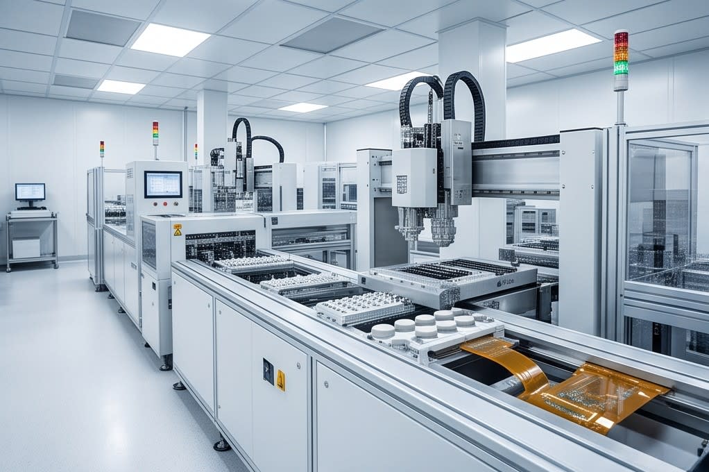
    ultra-fine semiconductor process line

    Technological Changes in Next-Generation Cleaning Processes

    A Paradigm Shift in the Cleaning Process

    As semiconductor integration has increased dramatically, the cleaning process now goes far beyond simple contaminant removal. In the past, washing away large visible particles was considered sufficient, but today, ultra-high-density components that require nanometer-level precision dominate the field.

    In this environment, the cleaning stage has become the most critical gateway determining product success. In line with these industrial demands, Huvics is presenting a next-generation cleaning standard model that combines proprietary ultrasonic dispersion technology with advanced vision inspection algorithms.

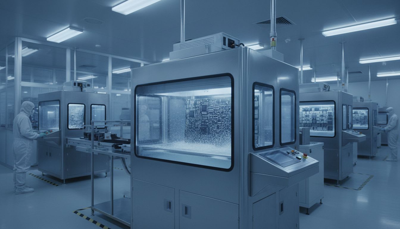
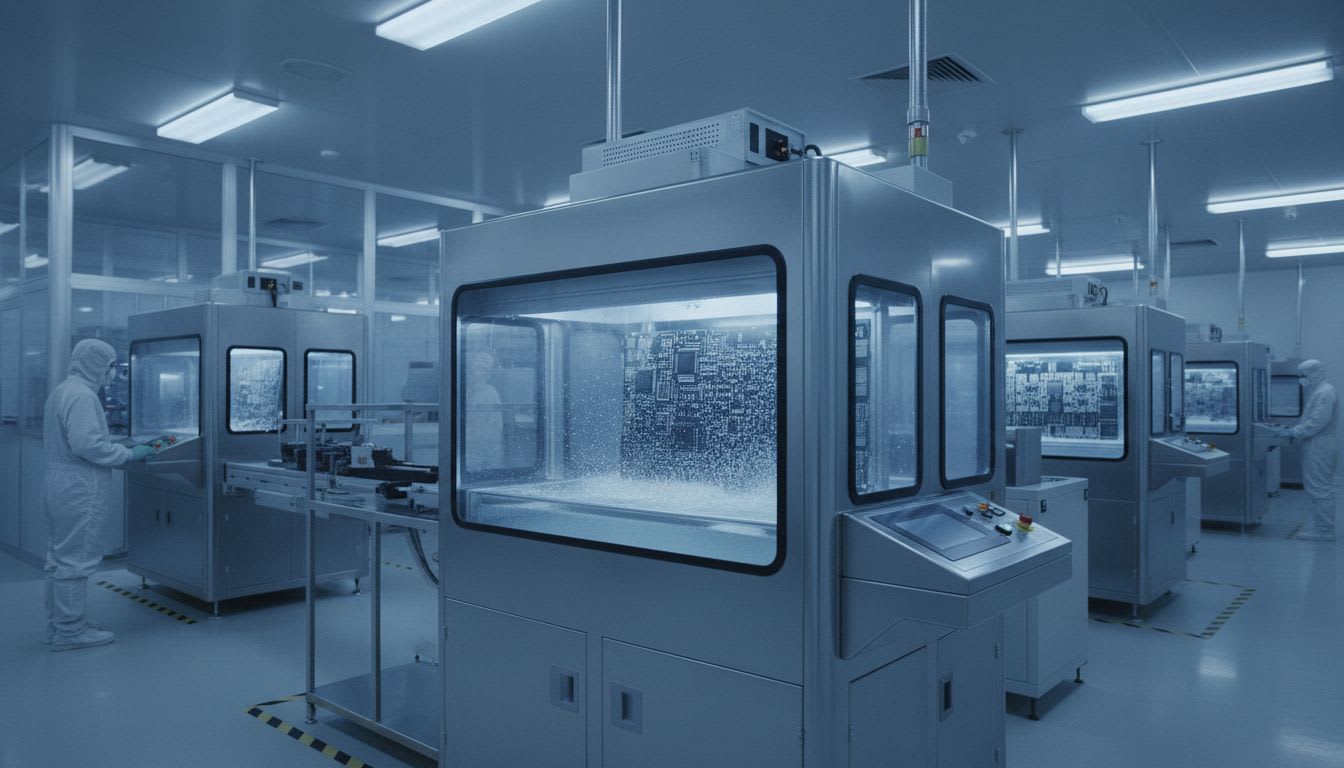
    intelligent automated cleanroom

    Securing Process Uniformity and an Intelligent System

    The core of our technology lies in precisely controlling material particles in liquid at the microscale to maximize uniformity across the entire process. This makes it possible to fundamentally eliminate the quality variability that has occurred in the manufacturing of high-density components.

    ultrasonic dispersion technology operation

    The new cleaning standard pursued by Huvics moves beyond the passive stage of simply washing away defects and takes a bold leap toward an intelligent process system that detects defects in fine patterns in real time and responds immediately. This process ultimately leads to a dramatic improvement in stability across the entire manufacturing process, while redefining the technological direction the next-generation semiconductor market must pursue.

    Core Competitiveness of the Huvics Solution

    Converged Solutions for Precision Manufacturing Sites

    In areas that require extreme precision, such as MLCC and FPCB manufacturing sites, the converged solution from Huvics demonstrates its strength. The key features of the Huvics solution are as follows.

    • Immediately detects fine defect factors through a real-time defect detection algorithm
    • Optimizes the dispersion of liquid materials using ultrasonic technology
    • Analyzes data in real time with an advanced vision inspection system

    Manufacturing Process Stability and Future Value

    This intelligent system autonomously controls the many variables that can arise during manufacturing, ultimately elevating the quality level of core components that determine the performance and durability of smart devices.

    semiconductor chip handling

    The innovative process system currently implemented by Huvics goes beyond simply improving work efficiency. As a new standard model for the next-generation semiconductor cleaning process, it will become a clear milestone for the industry’s future direction.

    This technological integration is becoming an important foundation for strengthening competitiveness across the semiconductor ecosystem by eliminating instability at manufacturing sites and raising the overall quality level of smart devices.

    fine patterns in ultra-high-density components

    The semiconductor cleaning process has now evolved beyond its past role of simple contaminant removal into a core intelligent system that determines the success of ultra-high-density components. The combination of ultrasonic dispersion technology and real-time vision inspection presented by Huvics is establishing a new quality standard that does not allow even the smallest variable within fine patterns.

    This process innovation fundamentally resolves instability at manufacturing sites and is rewriting the standard for high reliability that next-generation electronic components must achieve. We look forward to this precise integrated solution, which goes beyond technological limits, becoming a solid foundation that more reliably supports the smart devices in our daily lives.


    Huvics is an advanced technology company that develops and manufactures automation equipment and
    production systems across the semiconductor, LED, Mobile, and Cosmetic industries.
    With top talent and continuous technological innovation, we support customers in improving productivity and
    securing quality competitiveness.

    Huvics Contact

    Phone: 031-374-8285
    Email: cdpark@huvics.com
    Huvics inquiry

  • Semiconductor Back-End Process Innovation—Quality Reliability Achieved with Huvics Ultrasonic Dispersion and Precision Vision Inspection Solutions

    Semiconductor Back-End Process Innovation—Quality Reliability Achieved with Huvics Ultrasonic Dispersion and Precision Vision Inspection Solutions

    Huvics

    As semiconductors and electronic components enter an era of ultra-high integration that pushes beyond previous limits, even the smallest variables arising during the manufacturing process are becoming critical risks that determine the fate of finished products. In particular, controlling microscopic pattern distortion and foreign particles that cannot even be identified with the naked eye in advanced component production sites such as flexible printed circuit boards and multilayer ceramic capacitors is a core challenge that determines corporate survival.

    Recently, Huvics has been presenting a new standard in the back-end process field by directly addressing technical challenges with a unique convergence solution that combines ultrasonic energy and intelligent vision algorithms.

    Ultra-Precision Process Control Technology

    Quality Risks in the Era of High Integration and the Huvics Solution

    The semiconductor and electronic component markets are moving toward high integration that surpasses technological limits even at this moment. An era has arrived in which microscopic circuits and complex structures that were difficult to imagine in the past are naturally installed in everyday smart devices.

    Amid this trend, technology that controls minute quality variations in the back-end process field has become an absolute competitive advantage that determines the success or failure of companies. Huvics presents a unique technical solution to resolve quality risks that frequently occur in multilayer ceramic capacitor and flexible printed circuit board processes.

    Convergence of Ultrasonic and Vision Technology

    The core capability of Huvics begins with using ultrasonic energy to uniformly disperse key material particles inside liquids without gaps at the micro level. By intelligently combining this with a precisely designed vision inspection algorithm, Huvics has implemented a next-generation process control system that flawlessly detects everything from microscopic pattern distortion that cannot be identified with the naked eye to extremely small surface foreign particles.

    Defect Prevention Without Physical Damage

    Above all, the powerful distinction of Huvics lies in its ability to fundamentally prevent surface defects without causing physical damage to the fragile microstructures of substrates. This innovative solution dramatically improves the initial assembly reliability of advanced electronic components and serves as a solid technical foundation that enables customers to have confidence in production stability.

    Ultrasonic Material Dispersion Technology

    Advancement and Precision Control of the Laminating Process

    The laminating process proposed by Huvics goes beyond a simple stacking process and aims to become an advanced convergence solution that simultaneously performs uniform material dispersion and defect detection in microscopic patterns. Huvics takes the following approaches to improve process efficiency.

    • Precisely controls ultrasonic energy to evenly disperse particles inside liquids at the micro level
    • Adopts a substantial process approach that maximizes adhesion between materials
    • Identifies microscopic pattern distortion and surface foreign particles in real time through state-of-the-art vision algorithms

    Technology for Minimizing Physical Stress

    What is especially noteworthy is the unique control technology of Huvics that minimizes physical stress that may be applied to the fragile microstructures of substrates. In complex micro processes, even small vibrations or pressure changes can damage circuits, and the Huvics control system fundamentally prevents this.

    Meeting Process Efficiency and Quality Standards

    This precise control system, which improves defect detection accuracy while eliminating physical stress, plays a decisive role in dramatically raising the efficiency of the entire process. As a result, the technology of Huvics presents an ideal answer that fully satisfies the demanding quality standards customers face in highly complex and precise advanced device production environments.

    Precision Control System Structure

    Core Safety Mechanism for Improving Product Reliability

    This unique control system directly leads to improved reliability of final products. Today’s high-performance smart devices operate through the organic integration of microscopic components, so even a small defect rate in the initial assembly stage determines the performance and lifespan of finished products.

    A New Standard in the Back-End Process Field

    From this perspective, the fundamental surface defect prevention capability of Huvics is evaluated as presenting a new standard in the back-end process field. It is like a core safety mechanism that protects the strong assembly reliability customers must secure in the increasingly advanced electronic component market.

    Technology Partner for Customer Success

    The efforts of Huvics to realize the essential value of perfect quality beyond simple production yield improvement help customer products secure strong competitiveness in intense markets. As technology becomes more complex, manufacturing processes inevitably contain more variables, and Huvics controls this uncertainty through technology to create an environment where customers can focus solely on product innovation.

    The progress of Huvics in responding swiftly to changing market demands and advancing precise control systems strengthens its position not merely as an equipment partner but as a reliable partner that helps customers achieve successful product launches.

    Results of Perfect Quality

    In the world of electronic components that are becoming smaller and more complex while challenging technological limits, quality has now become a condition for survival that cannot be compromised. Huvics combines unique ultrasonic dispersion technology and sophisticated vision inspection to build unwavering reliability in strict process environments where even the smallest error is not allowed.

    The innovation of Huvics, which controls the uncertainty of complex manufacturing processes through technology, will become the most reliable foundation that helps customers focus solely on the essential competitiveness of their products. Together with Huvics, which answers changing market demands through precise control systems, we look forward to seeing your products make a higher and stronger leap in the next-generation device market.


    Huvics is an advanced technology company that develops and manufactures automation equipment and
    production systems across the semiconductor, LED, Mobile, and Cosmetic industries.
    With top talent and continuous technology innovation, Huvics supports customers in improving productivity and
    securing quality competitiveness.

    Huvics Contact Information

    Phone: 031-374-8285
    Email: cdpark@huvics.com
    Contact Huvics