The old semiconductor cleaning rule of simply washing well is no longer enough. This may sound somewhat exaggerated, but any production site that has directly experienced the critical defect rate and yield loss caused by even a single droplet of microscopic residual moisture will know that it is far from an empty claim. Then, from the perfect first cleaning step to flawless final drying, are we really following the right sequence? Let us examine the answer through the core solutions of Huvics, which is transforming cleanliness in semiconductor manufacturing sites and presenting a unique paradigm for yield improvement.
Proprietary Microbubble Cleaning Without Damage to Precision Surfaces
The First Step in Removing Microscopic Contamination
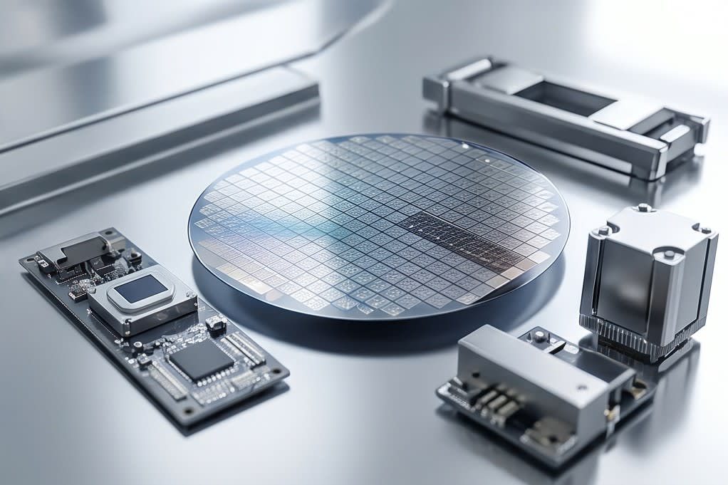
In the semiconductor manufacturing process, the first key step to check in order to achieve perfect yield is the cleaning process that completely removes microscopic contaminants from component surfaces. Semiconductors are an extremely sensitive field where even a single tiny dust particle can disable an entire circuit, so it is no exaggeration to say that the completeness of the cleaning process determines the life of the product. Huvics presents its proprietary microbubble technology as the first step of the process to completely remove even invisible microscopic contamination without causing the slightest damage to the precise surface of components. This is how the technology works.
- Generates microbubbles and allows them to penetrate complex gaps
- Weakens the bonding force between contaminants and the surface, lifting them upward
Precise Contaminant Removal Through High-Pressure Water Jet Technology
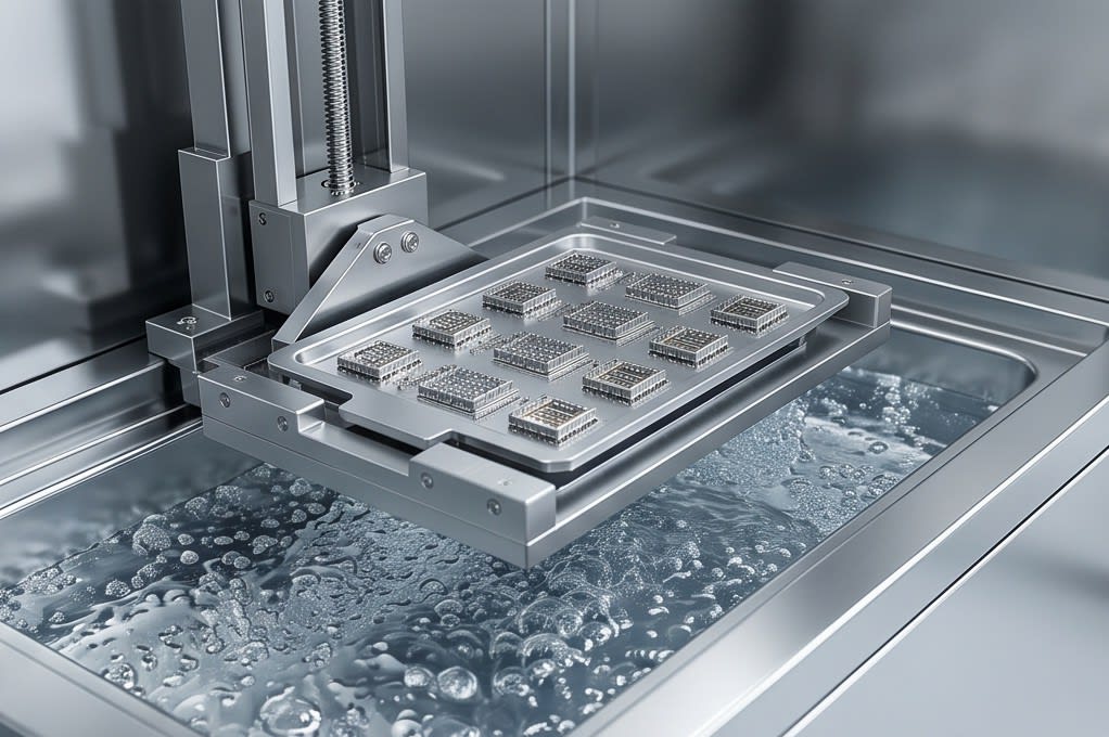
The microscopic contaminants lifted in this way then meet precisely operated high-pressure water jet technology. The high-pressure water jet safely and reliably separates only the microscopic particles that had been strongly attached to the machined surface of the component by striking them with exceptional precision. The core of the unique technical strength of Huvics lies in selectively separating only contaminants without causing any physical deformation or microscopic scratches to the precise original shape of the component. This is why many demanding semiconductor manufacturing sites experience a different level of cleanliness from the basic stage after introducing Huvics cleaning solutions and find a breakthrough for yield improvement.
Two-Step High-Performance Drying Process That Fundamentally Resolves Residual Moisture
Two-Step High-Performance Drying Process
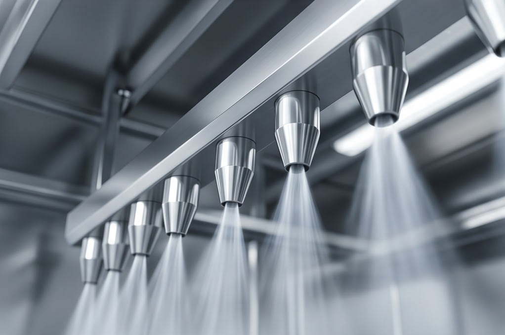
No matter how successfully a perfect cleaning process has been completed, if fast and proper drying is not carried out organically immediately afterward, all the effort invested can quickly be wasted. In fact, the most persistent limitation in conventional cleaning processes has been the problem of microscopic residual moisture remaining on component surfaces immediately after cleaning. If the process continues without fully removing moisture, stains can form on the surface or microscopic corrosion can progress, seriously reducing component reliability. To fundamentally resolve this residual moisture issue, Huvics implements a unique two-step high-performance drying process that tightly integrates high-speed air knife and high-temperature oven drying technologies. The detailed process steps are as follows.
- Immediately removes the water film on the surface with a high-speed air knife
- Evaporates moisture even in microscopic areas through high-temperature oven drying
Perfect Drying of Three-Dimensional Components
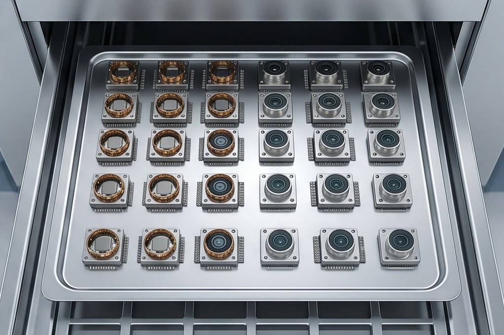
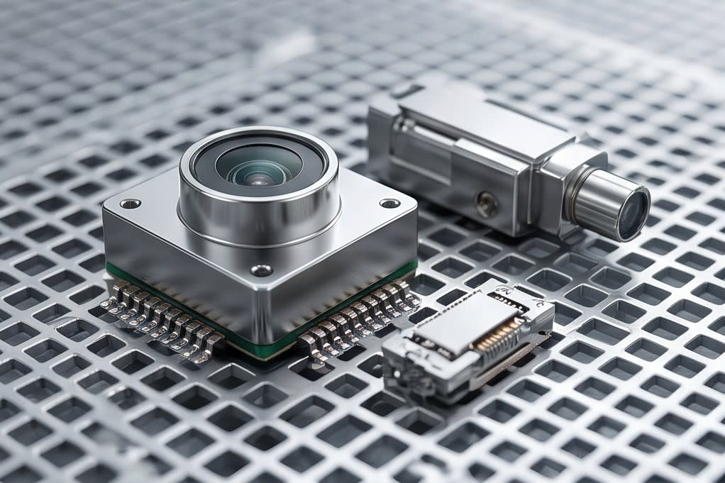
This precise two-step continuous process goes beyond simply wiping away water and serves as a powerful technical barrier that fundamentally blocks the possibility of secondary stains and microscopic corrosion that can easily occur after cleaning. In particular, it perfectly dries components with challenging three-dimensional shapes without structural limitations, such as camera modules, VCM motors with extremely complex internal structures, and transfer trays that precisely move components. This seamless drying method maximizes the lifespan and operational stability of components and final finished products, clearly proving to operators that the drying step is just as decisive as cleaning in determining the completion quality of the final product.
Moisture Zeroing and Final Verification for Even Complex Structures
Targets Requiring Precision Verification
The final stage encountered through semiconductor cleaning and drying processes is final verification and practical application, which stably proves uniform and consistent quality regardless of the complex shapes and geometric structures of components. In particular, the difficult targets that can easily cause critical defects when moisture remains are as follows.
- VCM motors with extremely complex internal structures
- Transfer trays that safely move microscopic components
- Camera modules that require precise assembly and management
Moisture Zeroing in Shadowed Areas
The high-performance cleaner system from Huvics perfectly realizes moisture zeroing by thoroughly detecting even shadowed areas that are difficult to confirm with the human eye or ordinary equipment and completely removing residual moisture, even in components with such complex and precise structures. This rigorous drying quality, which does not allow even a single droplet of microscopic moisture, becomes the driving force that dramatically improves the durability of each component in semiconductor microprocesses. As a result, it firmly guarantees the operational stability of equipment and provides a dependable foundation that dramatically extends the service life of final finished products. Beyond one-time cleaning that simply washes the surface of individual components, it provides a key differentiator directly connected to improving the yield of the entire production line, which semiconductor manufacturers manage with the greatest sensitivity. Ultimately, if you directly experience the series of systematic process steps that begin with precise first-stage cleaning technology and continue through final drying verification that allows no margin for error, you will deeply understand the overwhelming value that makes countless semiconductor manufacturing sites trust and choose Huvics as an irreplaceable and unique partner.
An Irreplaceable Choice for Perfect Yield Improvement
The frustration of seeing carefully cleaned components judged defective due to microscopic moisture stains and corrosion in a semiconductor manufacturing site is a serious concern that every field engineer has likely experienced at least once. The sequential solution from Huvics, which flows seamlessly from precise microbubble cleaning to flawless two-step drying, exists to completely resolve these real field challenges. Through thorough moisture zeroing that does not allow even a single droplet of moisture in complex three-dimensional shapes, we invite you to put aside concerns about defects and directly confirm unique production yield and the overwhelming stability of finished products.
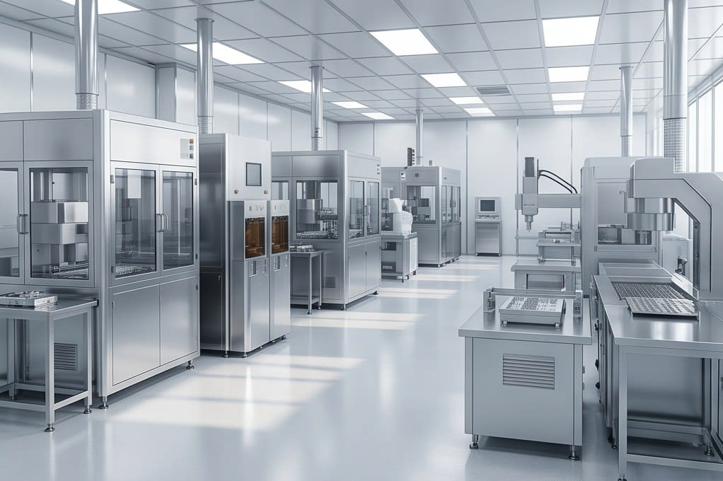
Huvics is an advanced technology company that develops and manufactures automation equipment and
production systems across the semiconductor, LED, mobile, and cosmetics industries.
With top talent and continuous technological innovation, Huvics supports customers in improving productivity and
securing quality competitiveness.
Huvics Contact
Phone: 031-374-8285
Email: cdpark@huvics.com