Tag: AISemiconductor

  • AI Semiconductor Packaging Yield: How to Improve It Step by Step from Grinding to Cleaning

    AI Semiconductor Packaging Yield: How to Improve It Step by Step from Grinding to Cleaning

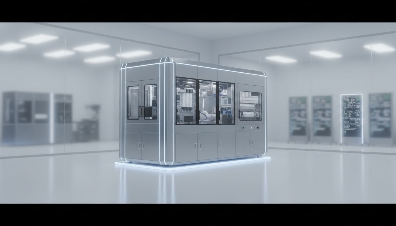
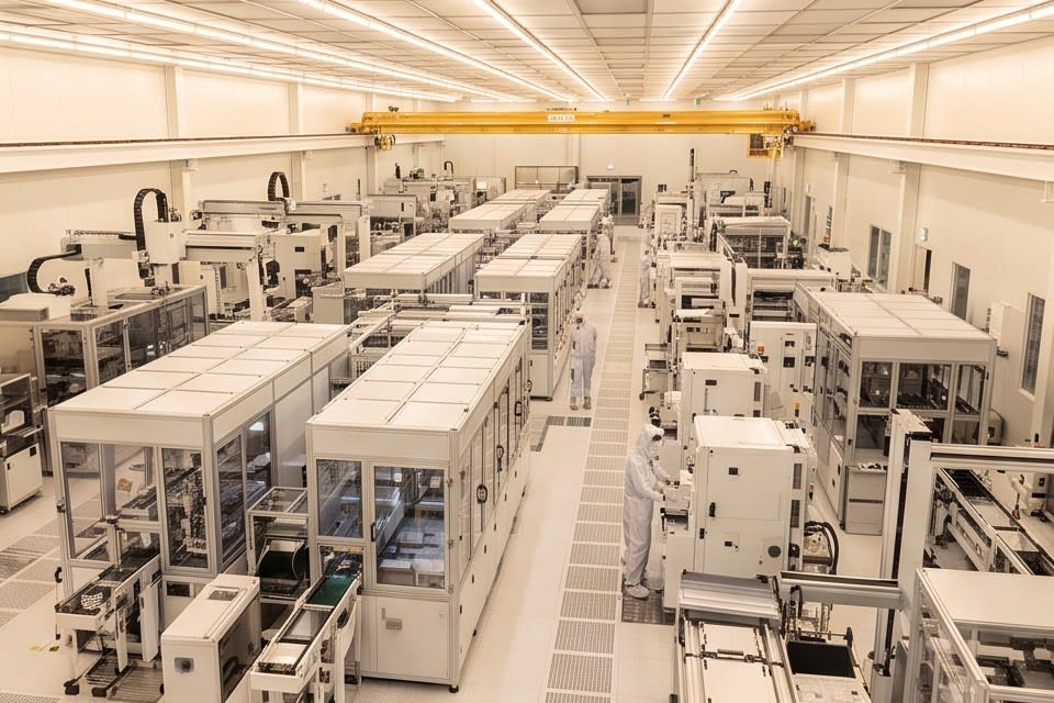
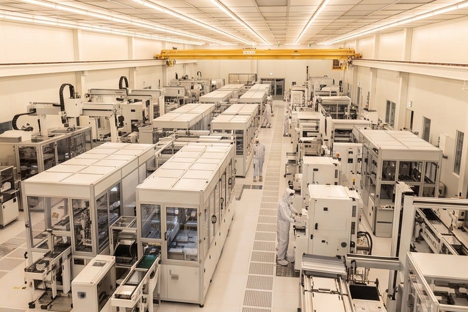
    A semiconductor packaging process site where multiple pieces of equipment are organically connected

    When I first looked closely at a semiconductor packaging site, there was one question customers commonly asked. “The grinding went well, so why do defects keep appearing during bonding?” That question once again confirmed that the root of the problem is not a single piece of equipment, but the entire flow of the process. At that site, I learned firsthand that even a slight deviation in flatness can affect every layer built on top of it.
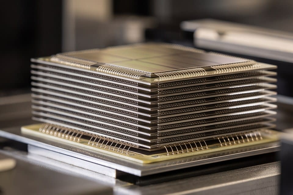
    A semiconductor stacked structure with dozens of dies precisely stacked vertically

    Why flatness is critical in AI semiconductor packaging

    HBM(High Bandwidth Memory), now a core component of artificial intelligence semiconductors, is built by vertically stacking dozens of thin dies. In a 12 layer stack, each die is about 50 micrometers thick, but when the stack increases to 16 layers, the die must be thinned to about 30 micrometers. As the die becomes thinner, the rigidity of the wafer itself decreases, and the risk of warpage and cracking during the process increases as well.

    Variation in surface flatness is not simply a dimensional issue. According to a technical report from Applied Materials, even minute surface variations directly affect bonding quality and yield. As the number of stacked layers increases, the requirements for thickness uniformity in each layer become stricter, and tolerances become narrower. As package types such as FCBGA, WLCSP, and QFN become more diverse, these requirements become even more complex. Ultimately, flatness control in the packaging process is not optional. It is a variable that determines yield itself.
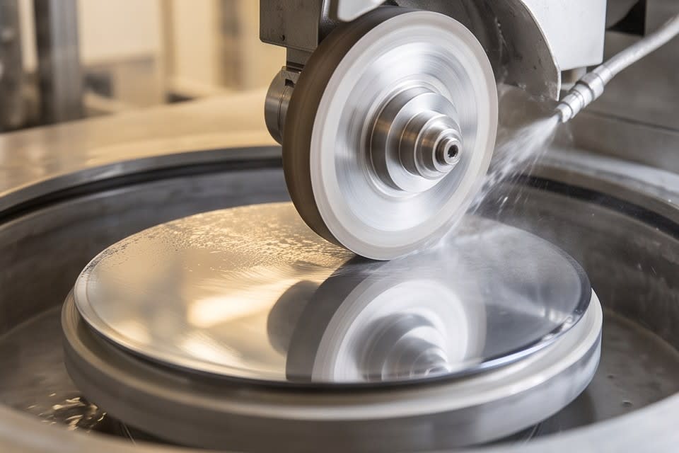
    A process scene in which a wafer surface is finely ground using a diamond wheel

    How the grinding process determines flatness

    The grinding process is a key step that determines the thickness and surface flatness of semiconductor dies. Unlike general cutting processes, precision grinding uses a diamond wheel to remove material in micron units while achieving the desired thickness and flatness at the same time. The tolerance achievable through precision grinding is around ±0.001~0.005mm, and surface roughness reaches Ra 0.2~0.8μm. This is 5~10 times more precise than general CNC milling.

    These figures matter not simply because they show how precise the process is, but because that precision directly determines the bonding quality of the subsequent bonding process. Grinding equipment that combines a high precision stage with a diamond wheel must be able to maintain thickness uniformity even in high speed processing. It is also important to have a configuration that allows flexible selection between fully automatic and manual types depending on the nature of the production line. Huvics PKG Grinder is designed to uniformly process various package types such as FCBGA, WLCSP, and QFN down to the thickness required by the customer. Choosing a grinding machine also means deciding the precision level for the entire process.
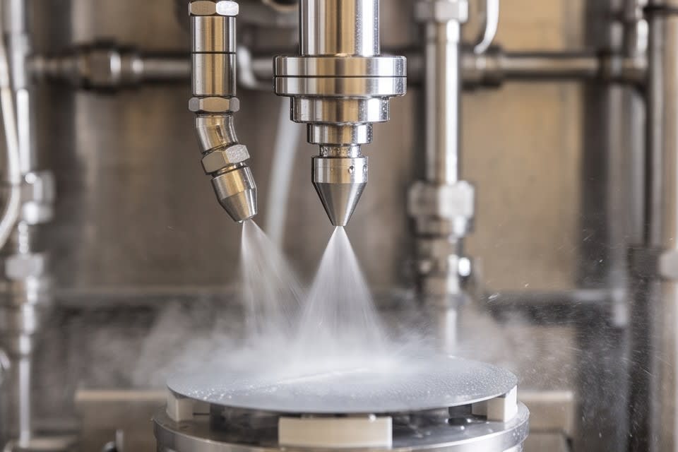
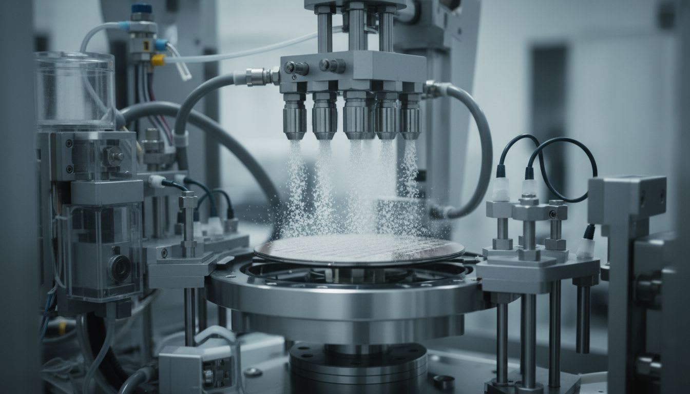
    A process of washing the die surface immediately after grinding by spraying cleaning liquid through a precision nozzle

    Why cleaning after grinding must be treated as one integrated step

    The die surface after grinding is in its most vulnerable state during the process. If fine particles and residues generated during grinding remain on the surface, they can lead to bonding defects in subsequent bonding or packaging steps.

    According to technical data from MSP/TSI, particle removal efficiency in the cleaning process is determined by multiple factors such as cleaning time, temperature, chemical concentration, and agitation method. How precisely these variables are controlled determines final quality. Simply rinsing with water makes it difficult to effectively remove residual particles at the submicron level.

    Huvics cleaning system uses a multi stage method that combines micro bubbles, water jets, and an air knife to remove surface contamination particles step by step, and its oven drying function handles residual moisture after cleaning. When analyzing the process of a customer who came with a camera module defect rate issue, repeated residual particles were occurring because the agitation conditions in the cleaning step had not been optimized. In semiconductor tray cleaning as well, the key was to design different cleaning conditions according to complex contamination types. This is exactly why how a surface precisely processed by grinding is finished in the cleaning step can completely change the value of the process.
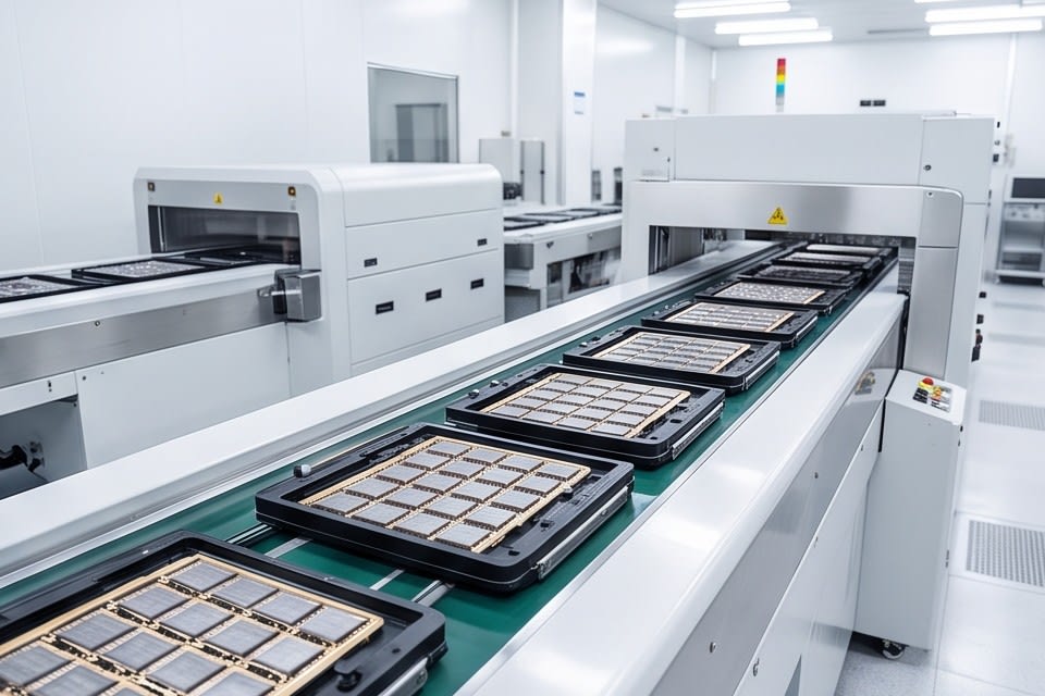
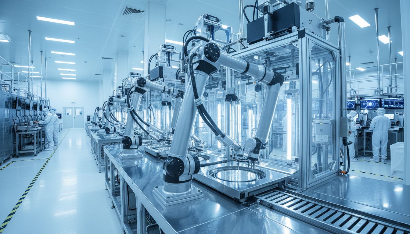
    Automated semiconductor process equipment organically connected along a conveyor belt

    The precision of the stacked structure required by AI semiconductors cannot be completed by the performance of grinding equipment alone. Only when cleaning can fully preserve the flatness created by grinding do those numbers truly have meaning. The two processes must be designed as one continuous flow. That is the real standard that determines packaging quality.


    Huvics is an advanced technology company that develops and manufactures automation equipment and
    production systems across the semiconductor, LED, Mobile, and Cosmetic industries.
    With top talent and continuous technological innovation, we support customers in improving productivity and
    securing quality competitiveness.

    Huvics Contact

    Phone: 031-374-8285
    Email: cdpark@huvics.com

    Huvics Inquiry

  • AI Semiconductor Cleaning, Micro Bubble vs Water Jet – What is the Optimal Method?

    AI Semiconductor Cleaning, Micro Bubble vs Water Jet – What is the Optimal Method?

    Are you dismissing the minor contamination occurring in the AI semiconductor production process as insignificant? If left unchecked because it is invisible, it may slow down production speeds slightly at first, but in the long run, it can lead to the following issues:

    • Productivity decline and quality issues due to increased defect rates
    • Rework and disposal costs leading to massive financial losses
    • An unforeseen crisis resulting in a decline in company credibility

    Huvics offers the optimal cleaning solution to address these potential risks and allow our clients to operate their AI semiconductor production lines more safely and efficiently.

    AI Semiconductor Cleaning’s Core: Micro Bubble and Water Jet

    Principles and Advantages of Micro Bubble Cleaning

    In the forefront of AI semiconductor production, cleaning technology is a critical factor that directly relates to the performance of the final product, transcending a mere process. This is because the complex structure of AI semiconductors, which are miniaturized from micron to nano scale, can lead to fatal defects from even a small particle of contamination. Against this backdrop, micro bubble cleaning excels by penetrating deeply into the gaps of micro-patterns on the wafer surface, using micro bubbles sized from hundreds of microns to a few nanometers, to gently separate contaminants like a precision spa ampoule removing impurities deep within the skin. This provides excellent cleaning effects while minimizing physical impact, making it ideal for high-density AI semiconductor circuits that are extremely sensitive to surface damage, significantly reducing the risk of wafer damage, decreasing defect rates, and increasing production yield.

    Features and Strengths of Water Jet Cleaning

    On the other hand, water jet cleaning presents the following strengths:

    • Effectively removes large particle contaminants and residues adhered to the surface with powerful water pressure
    • Increases efficiency for high-volume production with swift contaminant processing during manufacturing

    Huvics deeply acknowledges the importance of these two cleaning technologies, providing a multi-step cleaning solution optimized for the client’s AI semiconductor production environment, helping reduce defect rates and guaranteeing final quality stability.

    Criteria for Choosing Optimal Cleaning Technology: Target Characteristics and Yield Goals

    Core Criteria for Cleaning Technology Selection

    Each cleaning technology has its unique strengths. So, what criteria should our company use to make the best choice for AI semiconductor production? The key is to clearly define the ‘characteristics of the cleaning target’ and the ‘final yield goals’.

    For example, with high-performance AI semiconductor wafers that have extremely detailed and complex patterns, precision is crucial for cleaning. In this case, micro bubble cleaning, which removes fine contaminants without physical damage, is far more advantageous in ensuring wafer integrity and maximizing final yield. Minimizing the risk of surface damage, reducing the likelihood of malfunctions or damage to fine circuits, is important.

    Conversely, for processes where patterns are relatively less complex or where larger particle contaminants need rapid removal, the powerful cleaning capability of water jet technology can be a more efficient solution. Huvics does not stubbornly adhere to a single cleaning technology, but instead proposes customized cleaning solutions by thoroughly analyzing the product type, production environment, and required yield goals. Properly understanding our product’s characteristics and choosing the optimal cleaning method is key to securing competitiveness in the AI semiconductor market.

    Choosing Cleaning Technology from a Long-term Perspective: Total Cost of Ownership (TCO) Analysis

    TCO Analysis of Water Jet Cleaning

    In addition to considering the characteristics of the cleaning target and the yield goals, choosing a cleaning technology should be a strategic decision, not based solely on initial investment costs. Water jet cleaning’s relatively low initial equipment cost and rapid cleaning capability are clear strengths. However, the possibility of micro physical impacts on the wafer surface from high water pressure is an unignorable risk factor for sensitive products like AI semiconductors. Such micro damages, though not immediately noticeable, can lead to increased defect rates and reduced yield in the long run, acting as ‘hidden costs’ that ultimately raise production costs.

    Long-term Economics of Micro Bubble Cleaning

    Conversely, the initial investment cost of micro bubble cleaning may be higher. However, by minimizing wafer damage and achieving high yields, it can be a much more economical choice in the long term. This improves final product quality stability, enhances client market credibility, and reduces rework and disposal costs. From the perspective of total cost of ownership (TCO), Huvics thoroughly analyzes the pros and cons of each cleaning technology, providing solutions that align with the client’s production goals and long-term vision. Beyond simply equipment sales, Huvics aims to be a steadfast partner in the sustainable growth and technological innovation of the client’s successful future in AI semiconductor production.

    In AI semiconductor production, the choice of cleaning technology transcends mere process, being a key strategic decision that mitigates potential losses, ensures high yield, and enhances market competitiveness. Understanding the clear differences in the sensitivity of micro bubbles and the strength of water jets, and finding the optimal method that most aligns with our product’s characteristics and goals, is crucial. As a reliable partner to solve these concerns, Huvics provides customized multi-step cleaning solutions, guiding the way to stable, high-quality AI semiconductor production. Now is the time to confidently select the best choice and seize the future of the AI semiconductor market.


    Huvics is a high-tech company developing and manufacturing automation equipment and
    production systems across the semiconductor, LED, Mobile, and Cosmetic industries.
    With top-tier talents and continuous technological innovation, we support clients in improving productivity and
    securing quality competitiveness.

    Contact Huvics Co., Ltd.

    Phone: 031-374-8285
    Email: cdpark@huvics.com
    Contact Huvics