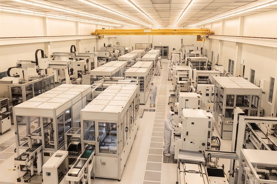
When I first looked closely at a semiconductor packaging site, there was one question customers commonly asked. “The grinding went well, so why do defects keep appearing during bonding?” That question once again confirmed that the root of the problem is not a single piece of equipment, but the entire flow of the process. At that site, I learned firsthand that even a slight deviation in flatness can affect every layer built on top of it.
Why flatness is critical in AI semiconductor packaging
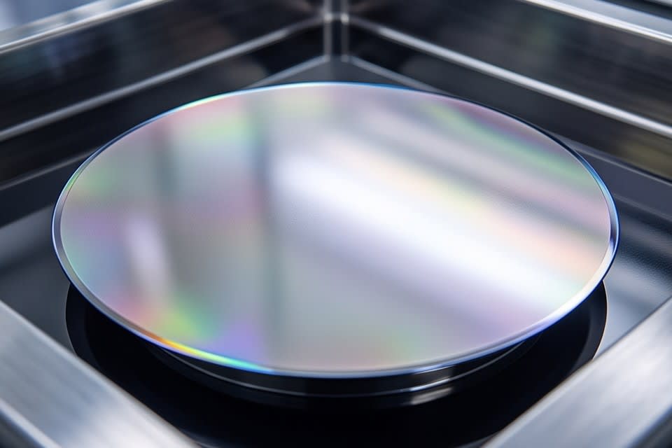
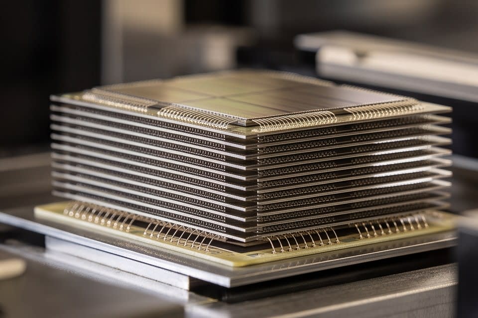
HBM(High Bandwidth Memory), now a core component of artificial intelligence semiconductors, is built by vertically stacking dozens of thin dies. In a 12 layer stack, each die is about 50 micrometers thick, but when the stack increases to 16 layers, the die must be thinned to about 30 micrometers. As the die becomes thinner, the rigidity of the wafer itself decreases, and the risk of warpage and cracking during the process increases as well.
Variation in surface flatness is not simply a dimensional issue. According to a technical report from Applied Materials, even minute surface variations directly affect bonding quality and yield. As the number of stacked layers increases, the requirements for thickness uniformity in each layer become stricter, and tolerances become narrower. As package types such as FCBGA, WLCSP, and QFN become more diverse, these requirements become even more complex. Ultimately, flatness control in the packaging process is not optional. It is a variable that determines yield itself.
How the grinding process determines flatness
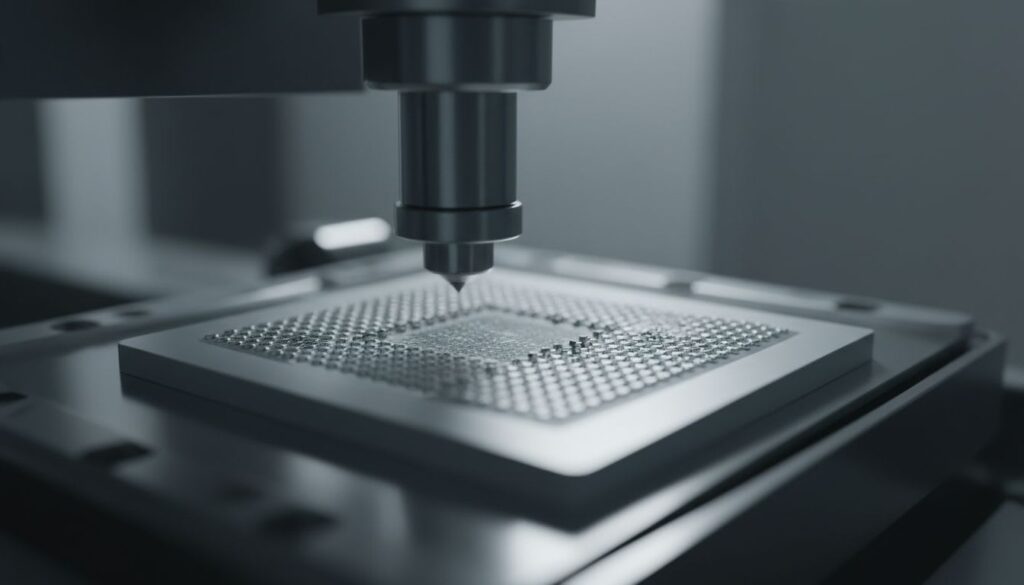
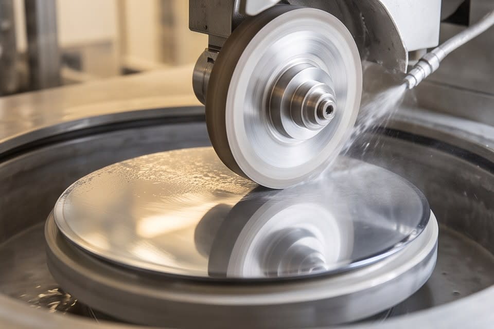
The grinding process is a key step that determines the thickness and surface flatness of semiconductor dies. Unlike general cutting processes, precision grinding uses a diamond wheel to remove material in micron units while achieving the desired thickness and flatness at the same time. The tolerance achievable through precision grinding is around ±0.001~0.005mm, and surface roughness reaches Ra 0.2~0.8μm. This is 5~10 times more precise than general CNC milling.
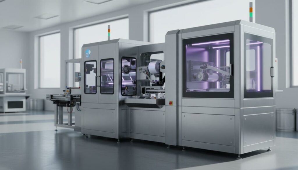
These figures matter not simply because they show how precise the process is, but because that precision directly determines the bonding quality of the subsequent bonding process. Grinding equipment that combines a high precision stage with a diamond wheel must be able to maintain thickness uniformity even in high speed processing. It is also important to have a configuration that allows flexible selection between fully automatic and manual types depending on the nature of the production line. Huvics PKG Grinder is designed to uniformly process various package types such as FCBGA, WLCSP, and QFN down to the thickness required by the customer. Choosing a grinding machine also means deciding the precision level for the entire process.
Why cleaning after grinding must be treated as one integrated step
The die surface after grinding is in its most vulnerable state during the process. If fine particles and residues generated during grinding remain on the surface, they can lead to bonding defects in subsequent bonding or packaging steps.
According to technical data from MSP/TSI, particle removal efficiency in the cleaning process is determined by multiple factors such as cleaning time, temperature, chemical concentration, and agitation method. How precisely these variables are controlled determines final quality. Simply rinsing with water makes it difficult to effectively remove residual particles at the submicron level.
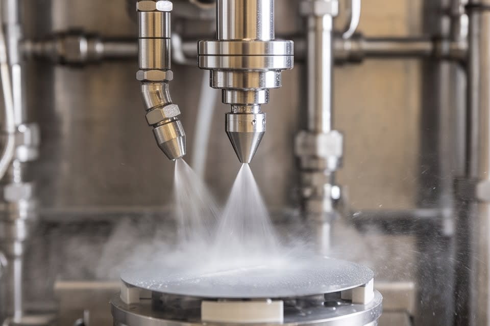
Huvics cleaning system uses a multi stage method that combines micro bubbles, water jets, and an air knife to remove surface contamination particles step by step, and its oven drying function handles residual moisture after cleaning. When analyzing the process of a customer who came with a camera module defect rate issue, repeated residual particles were occurring because the agitation conditions in the cleaning step had not been optimized. In semiconductor tray cleaning as well, the key was to design different cleaning conditions according to complex contamination types. This is exactly why how a surface precisely processed by grinding is finished in the cleaning step can completely change the value of the process.
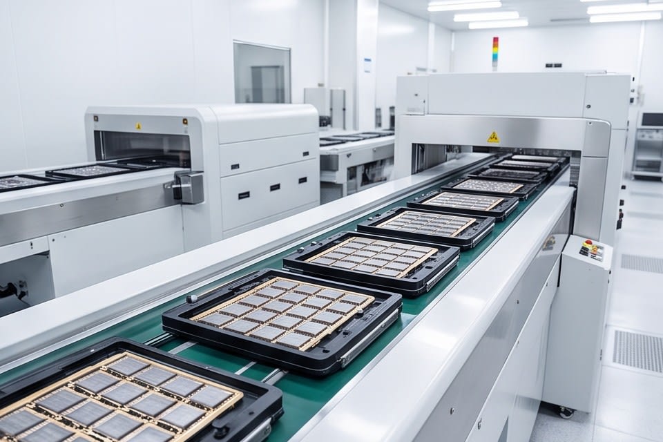
The precision of the stacked structure required by AI semiconductors cannot be completed by the performance of grinding equipment alone. Only when cleaning can fully preserve the flatness created by grinding do those numbers truly have meaning. The two processes must be designed as one continuous flow. That is the real standard that determines packaging quality.
Huvics is an advanced technology company that develops and manufactures automation equipment and
production systems across the semiconductor, LED, Mobile, and Cosmetic industries.
With top talent and continuous technological innovation, we support customers in improving productivity and
securing quality competitiveness.
Huvics Contact
Phone: 031-374-8285
Email: cdpark@huvics.com