Tag: Semiconductor

  • A Field Case That Made the Difference Between 95% and 75% Yield, How Are You Designing Your Cleaning Process?

    A Field Case That Made the Difference Between 95% and 75% Yield, How Are You Designing Your Cleaning Process?

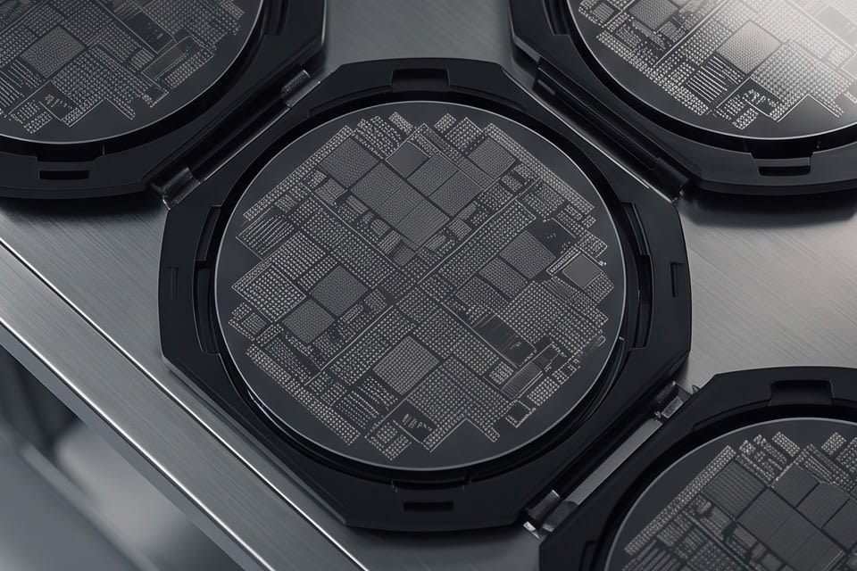
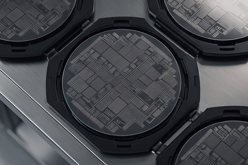
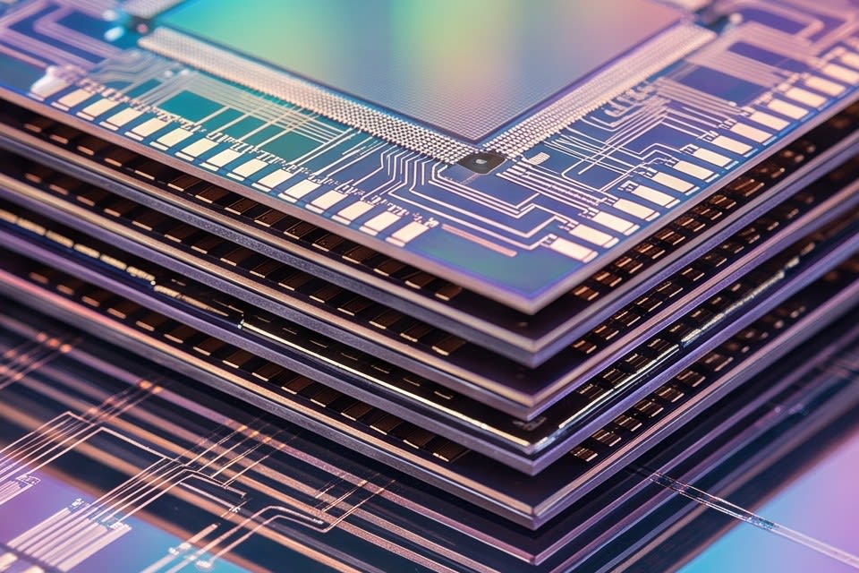
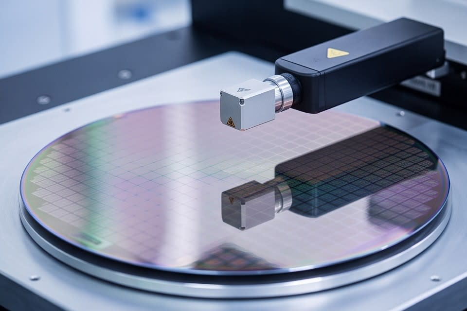
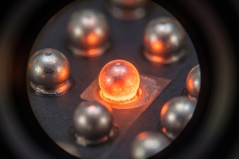
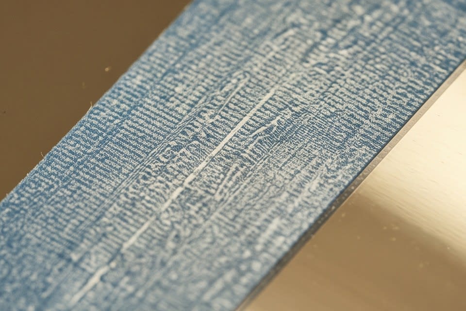
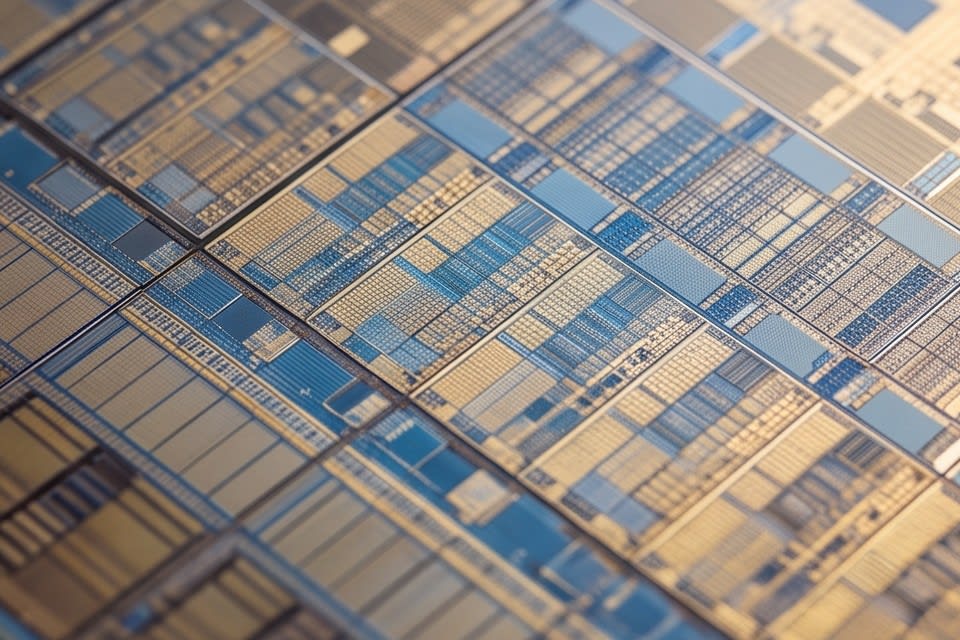
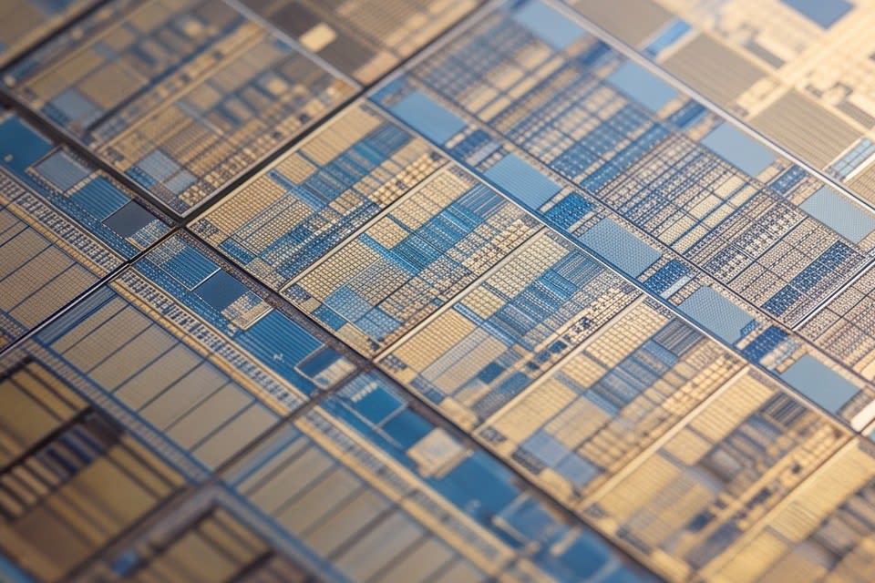
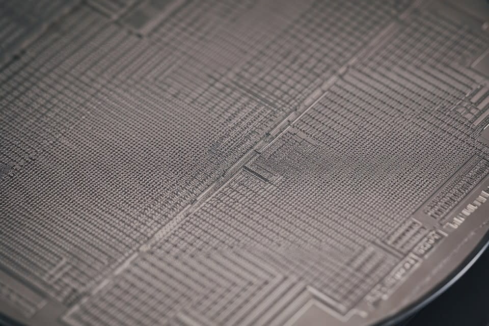
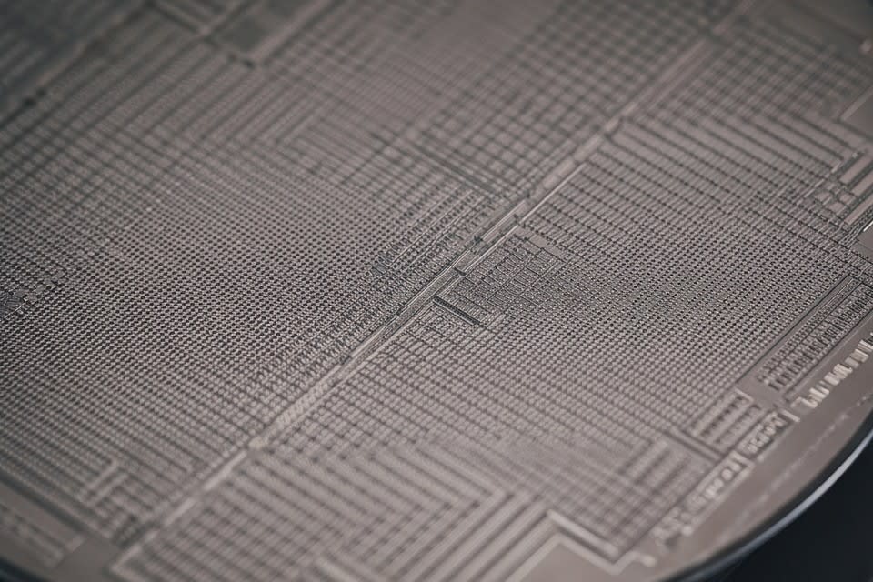
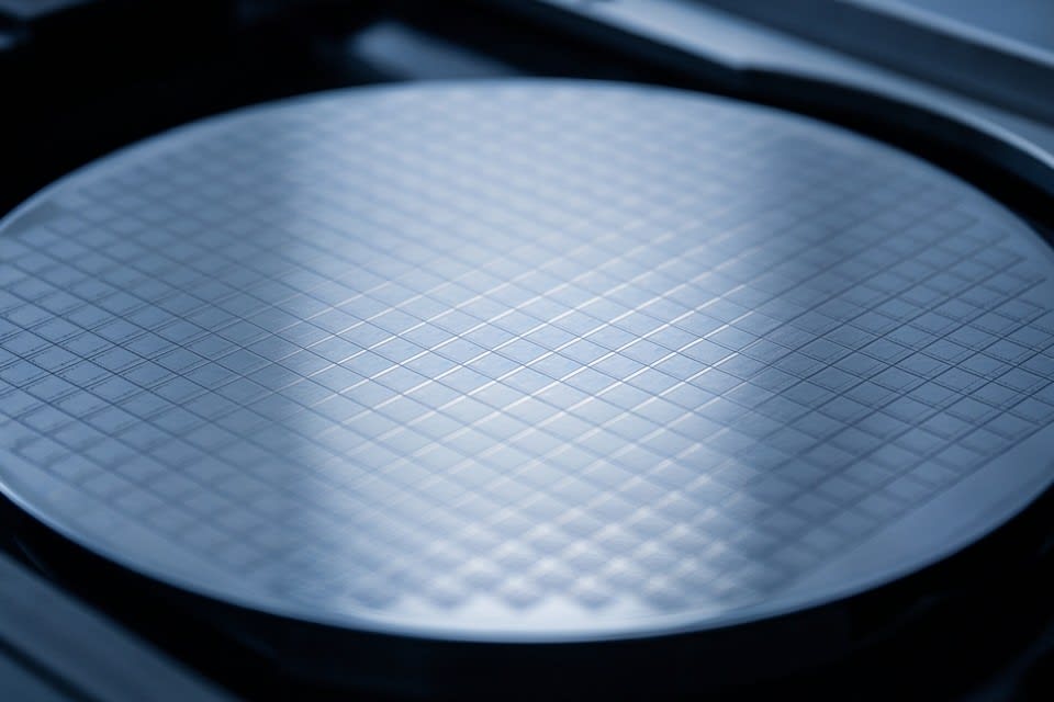
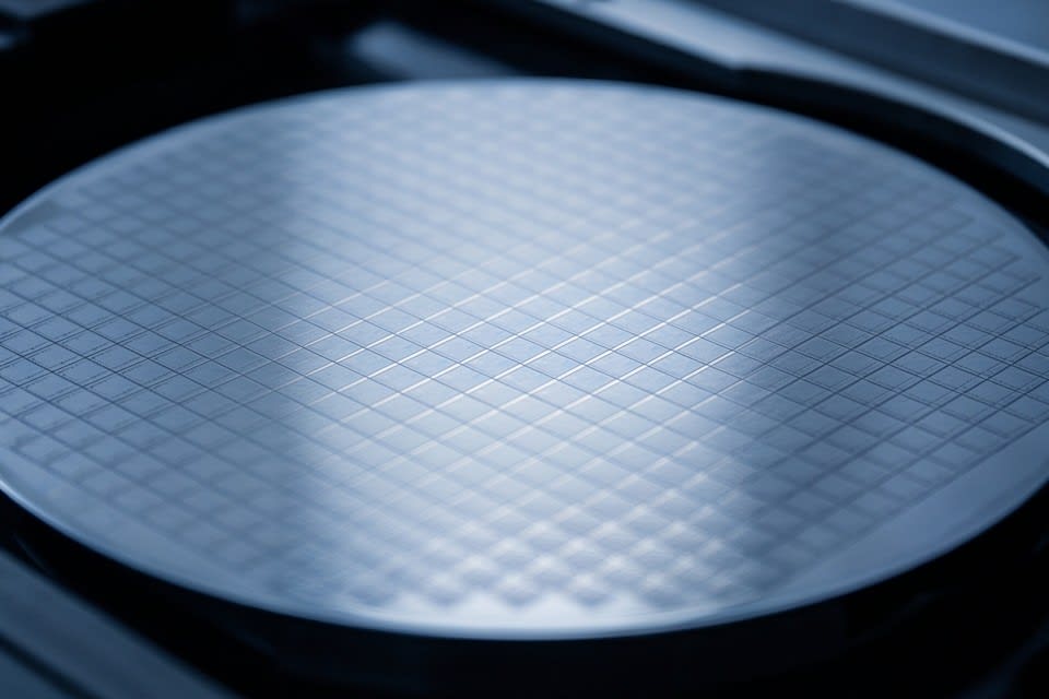
    Fine die structures on the surface of a wafer, a key material in semiconductor manufacturing

    In semiconductor manufacturing sites, some view the cleaning process as the ‘finishing stage’. However, the fact that a single contaminant particle can change the fate of an entire wafer shows that cleaning is not the end of the process, but a variable that determines yield.

    The Impact of a Single Contaminant Particle on Yield

    In semiconductor manufacturing, contaminant particles reduce yield in ways that cannot be seen with the naked eye. If a single submicron particle lands on a wafer during the photolithography process, the entire die can become unusable. According to Applied Physics USA, this is a real cause that separates a 95% yield from a 75% yield.

    As processes move down to 3 nanometers and 2 nanometers, the allowable contamination level becomes even narrower. A single contaminant particle can lead to the disposal of an entire wafer, and the resulting loss can reach millions of dollars. As processes become finer, the role of cleaning is elevated from simply maintaining cleanliness to serving as a line of defense for yield.

    No matter how well a cleanroom environment is prepared, particles generated during the process are targets for control, not something that can be considered completely eliminated. Ultimately, a clear trend has taken hold in semiconductor manufacturing sites, where final quality stability is determined by how cleaning equipment removes particles and at which stage it does so.
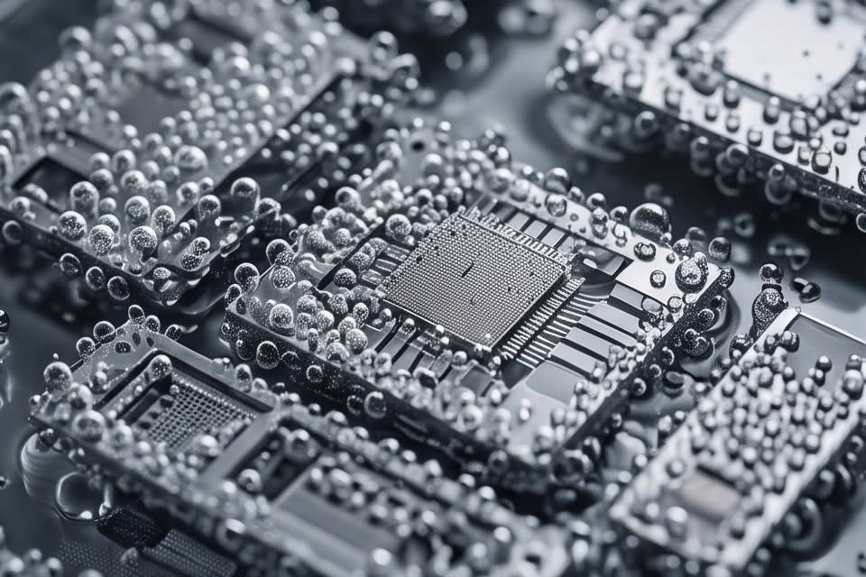
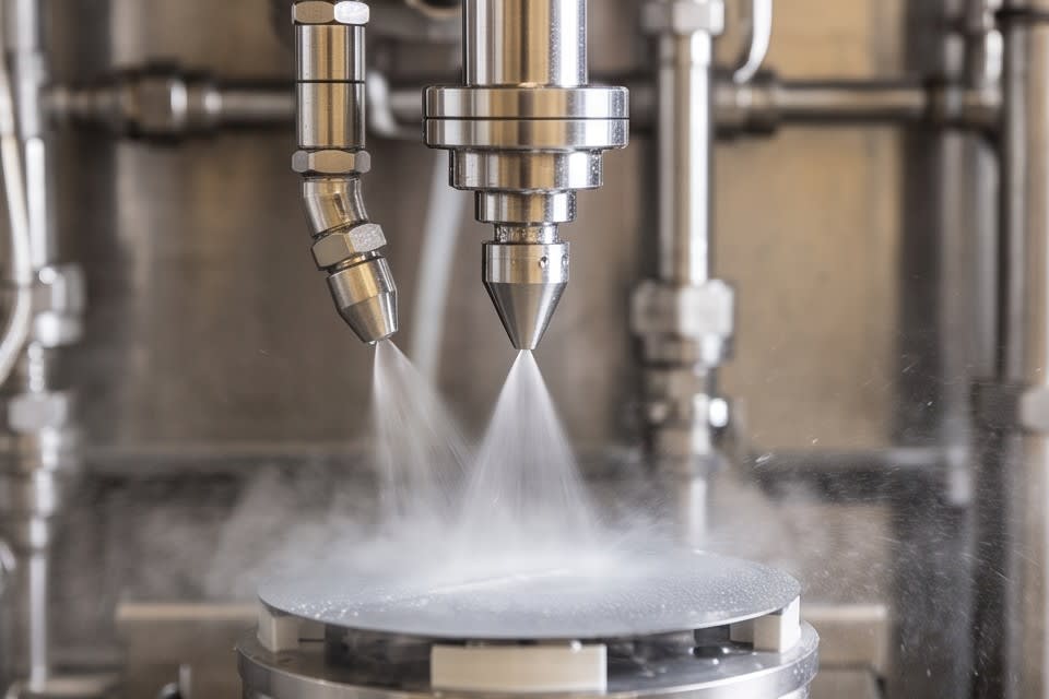
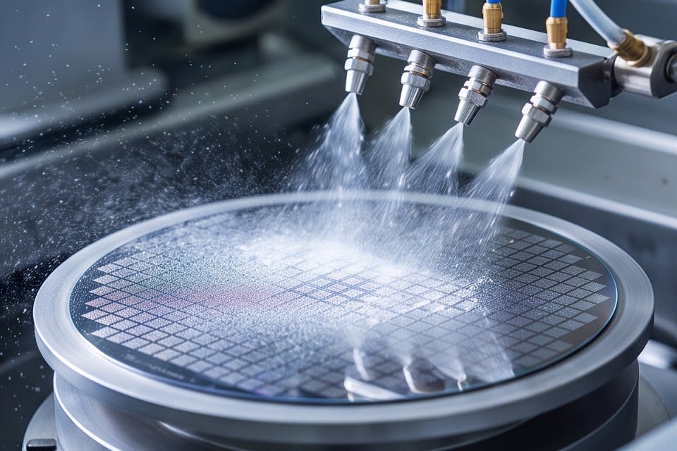
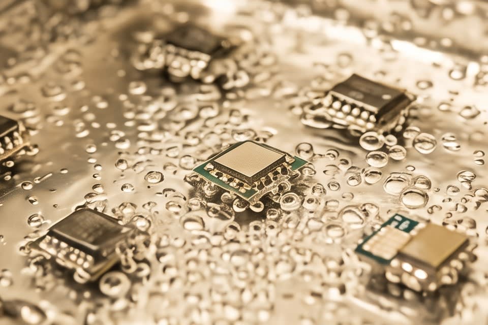
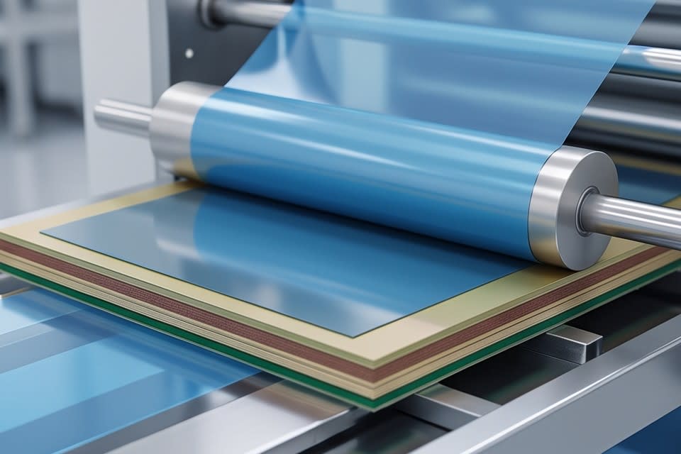
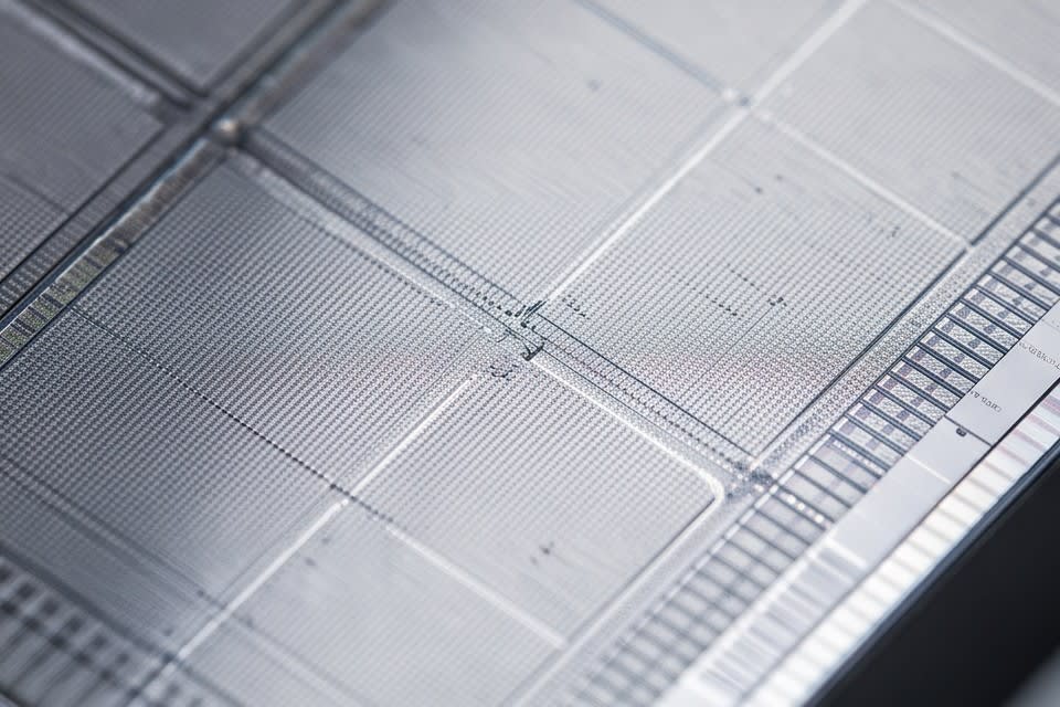
    Micro bubble cleaning method in which fine bubbles cover the surface of a semiconductor chip

    Structure and Role of Multi Step Cleaning Technology

    To effectively remove contaminant particles, a single cleaning method has limitations. This is because the nature of contamination varies, including particles loosely attached to the surface, foreign matter embedded in fine grooves, and residual liquids generated during the process. To address this, multi step cleaning methods are being adopted in the field.

    • Micro Bubble is a method in which fine bubbles contact the surface and separate particles without physical impact, making it suitable for removing contamination while minimizing surface damage to precision components.
    • Water Jet directly removes surface contamination using a high pressure water stream.
    • Air Knife blows away residual moisture after cleaning and prevents contamination from reattaching before the drying stage.
    • When the Oven Dry function is added, the process flow from cleaning to drying is completed as one integrated sequence.

    Huvics Cleaner System is designed so that this multi step configuration can be applied according to the characteristics of products such as camera modules, sensors, VCM motors, and trays, and it can be selected as either Full Auto or Manual depending on site conditions. When selecting cleaning equipment, the key is not a single performance figure, but a step configuration suited to the contamination type and product shape.
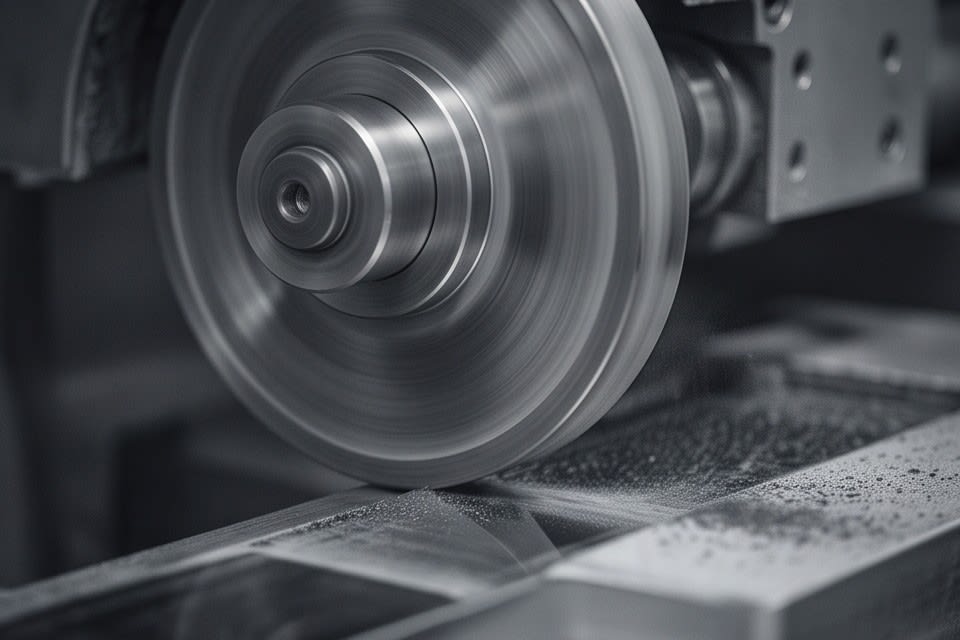
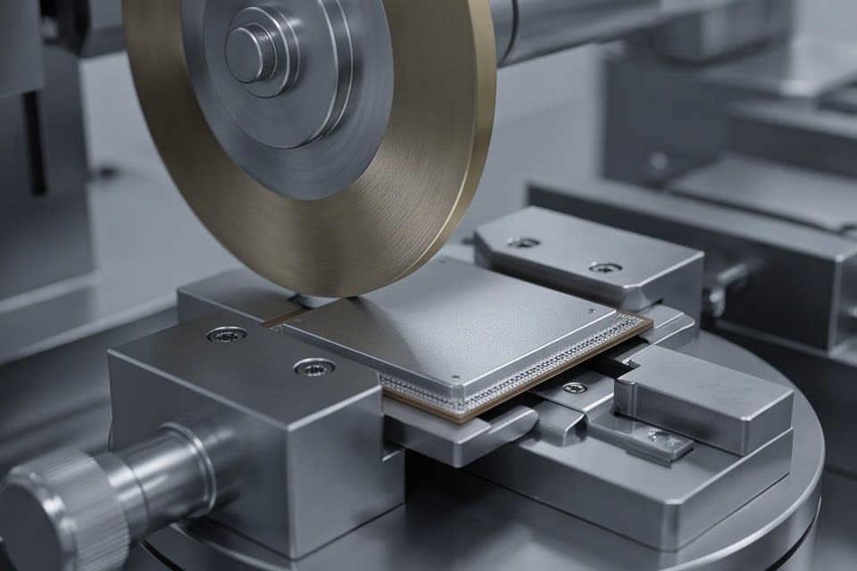
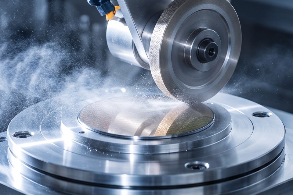
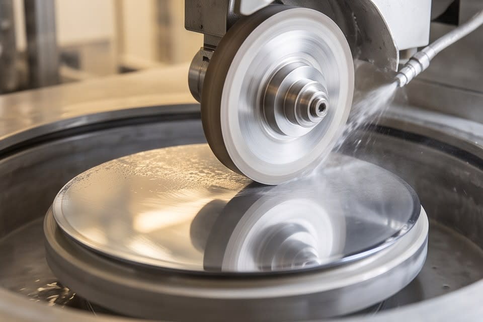
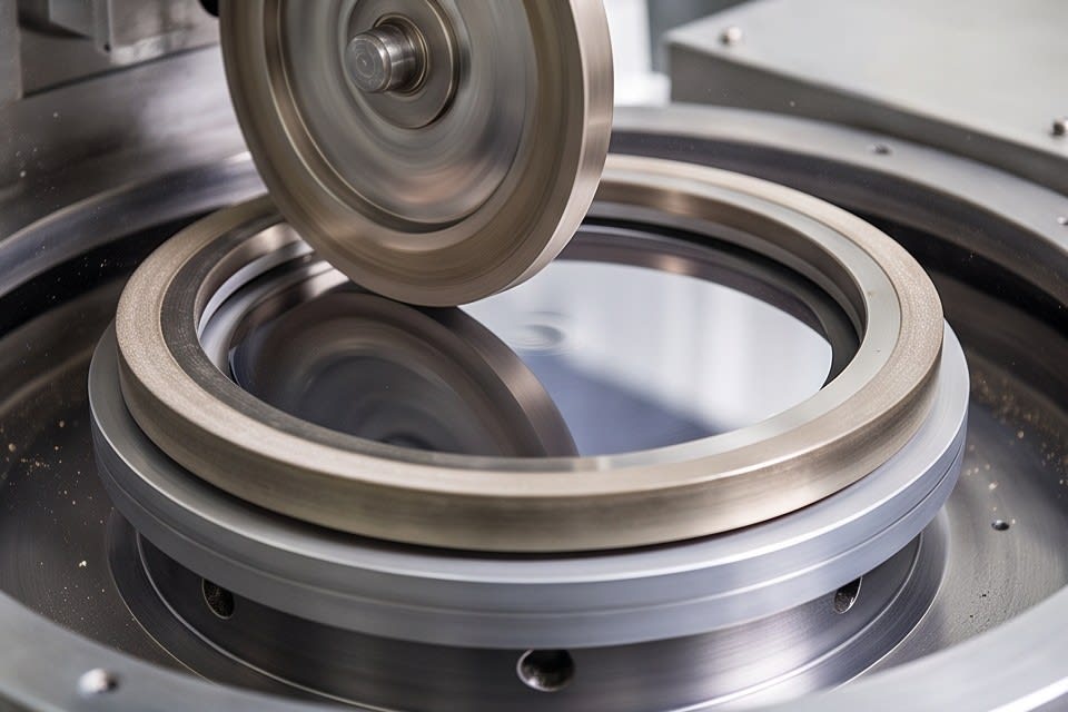
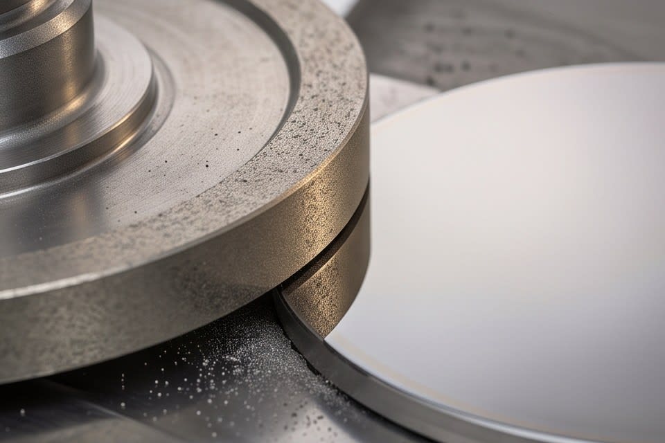
    A high speed rotating diamond wheel processing a semiconductor package at the micron level

    The Link Between Machining Precision and Cleaning Efficiency

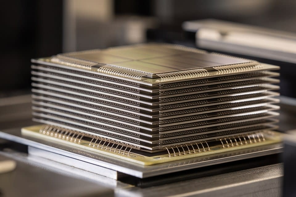
    Engineers responsible for chip stacking processes know very well how sensitive package thickness variation can be as a variable. In structures where dozens of chips are stacked vertically, such as AI semiconductors or high performance memory, the thickness uniformity and flatness of each layer are directly connected to signal transmission and bonding reliability. When thickness variation accumulates, it can lead to poor electrical connections or heat dissipation issues, which is like planting the seeds of yield loss even before the cleaning stage.

    Huvics PKG Grinder uses a high precision Stage and Diamond Wheel to achieve micron level thickness uniformity. It supports a wide range of package types, including FCBGA, WLCSP, QFN/DFN, and Solar Cell, and can reliably process products to the thickness targets required by customers. It supports both Full Auto and Manual modes, ensuring flexibility in production line configuration.

    By minimizing quality variation even in high speed processes, it creates the conditions needed to maximize the effectiveness of the subsequent cleaning process. Machining precision determines cleaning efficiency, and cleaning efficiency determines final yield. The significance of the PKG Grinder is confirmed by the fact that these two processes are connected.
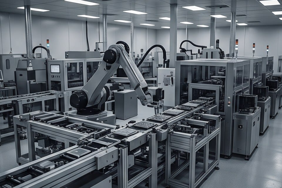
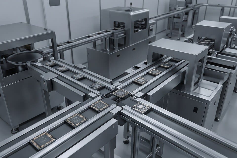
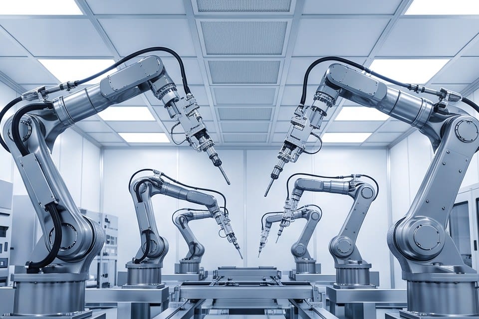
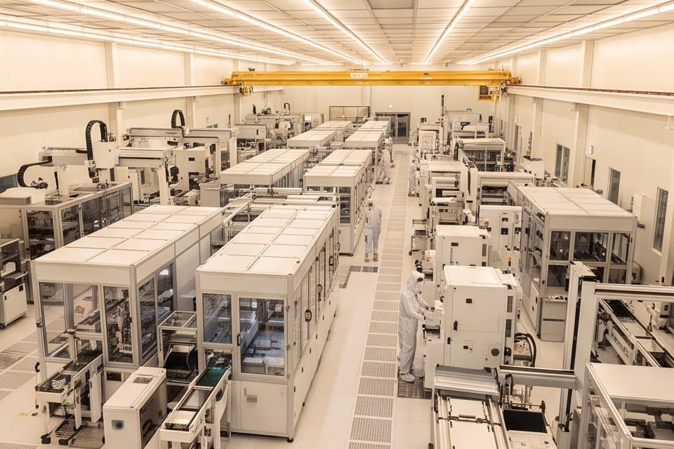
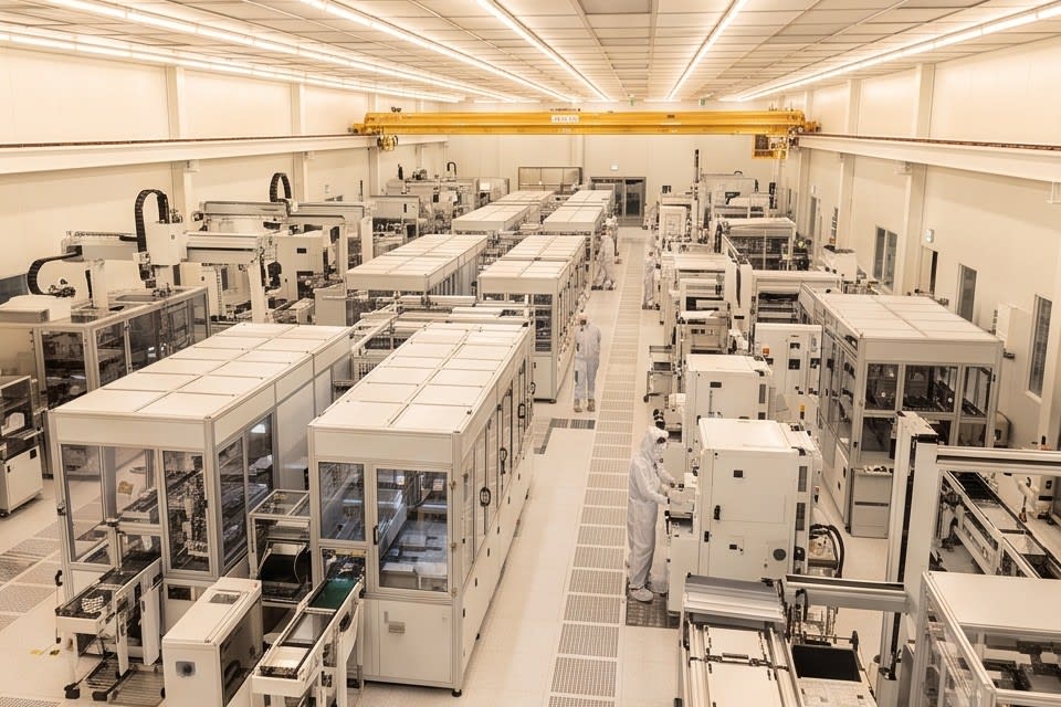
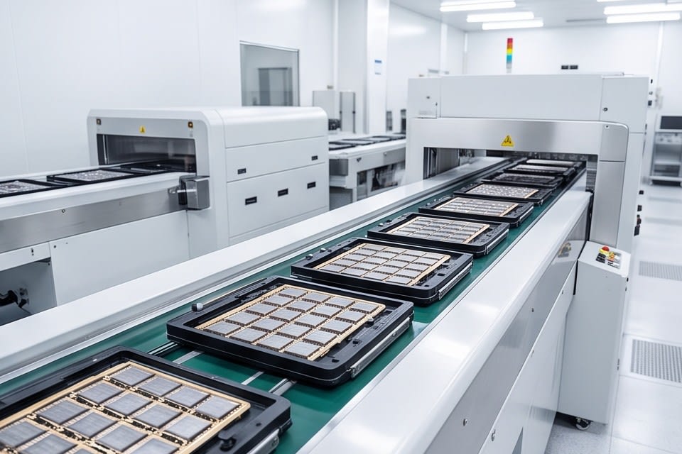
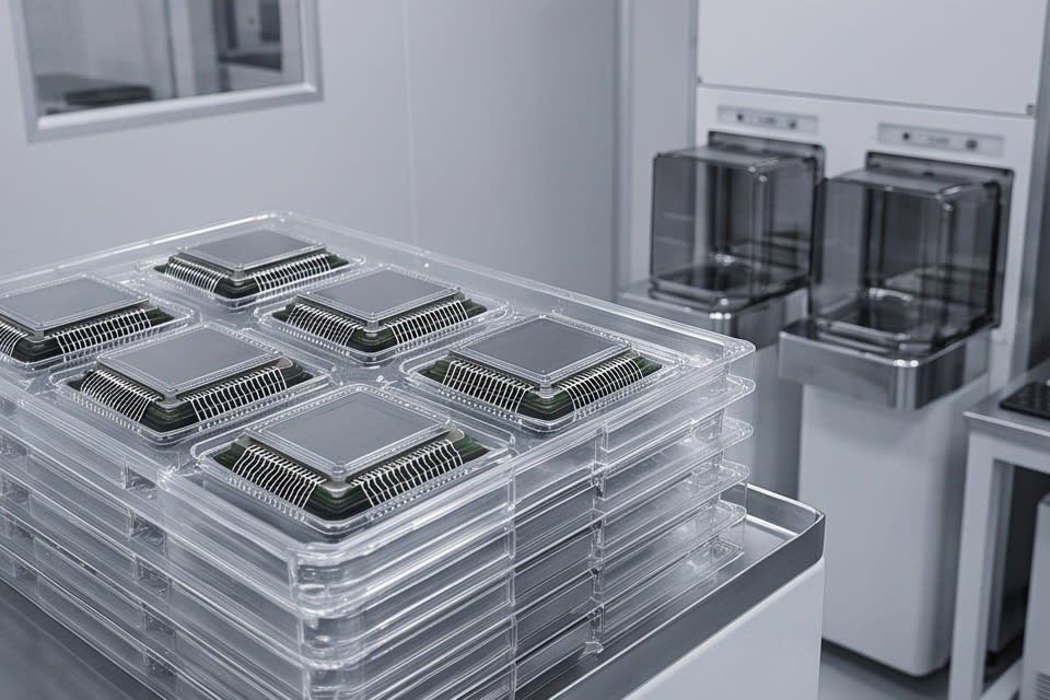
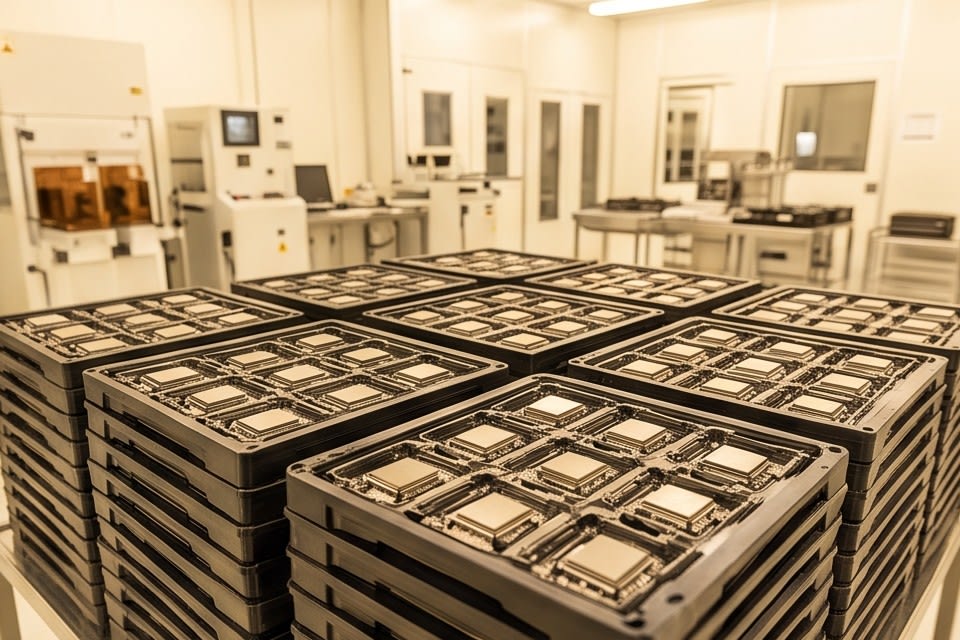
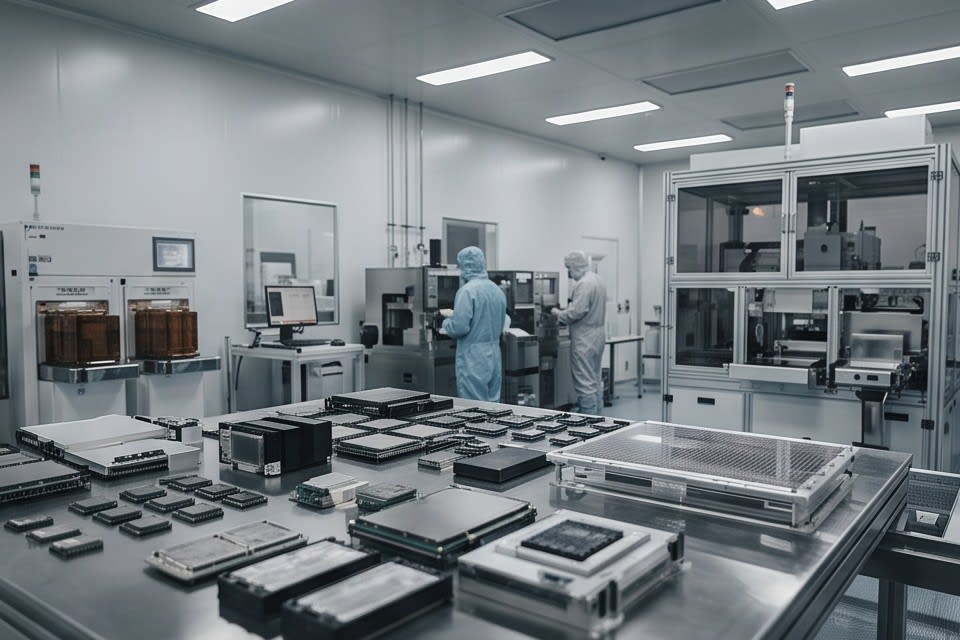
    Interior of a cleanroom with a multi step cleaning system and automated process line installed

    When choosing cleaning equipment, many people commonly focus only on cleaning power. However, because the type of contamination, the shape of the product, and the requirements of the subsequent process all differ, the criteria for equipment selection must also change. Understanding the structure in which machining precision supports cleaning efficiency and the cleaning method determines final yield is the starting point for semiconductor process design.


    Huvics is an advanced technology company that develops and manufactures automation equipment and
    production systems across the semiconductor, LED, Mobile, and Cosmetic industries.
    With top talent and continuous technological innovation, we support customers in improving productivity and
    securing quality competitiveness.

    Huvics Contact

    Tel: 031-374-8285
    Email: cdpark@huvics.com

    Huvics Inquiry

  • Introducing Custom Automation Equipment and How to Select Equipment by Process Stage

    Introducing Custom Automation Equipment and How to Select Equipment by Process Stage

    When considering the introduction of custom automation equipment, it is natural to feel unsure about where to begin. Each process has different requirements, and although there are many types of equipment, few sources clearly explain the criteria for choosing the right one. Add technical terms such as micron-level precision and yield, and it can easily feel overwhelming for those encountering them for the first time. It is completely normal for this to feel difficult. From here, we will break down that complex context step by step.

    A complex fine wire bonding semiconductor chip showing an ultra-precision manufacturing environment

    Why custom automation equipment has become essential

    Today, manufacturing sites that produce ultra-precision components such as semiconductors, camera modules, and autonomous driving sensors operate under conditions completely different from just a few years ago. Components are becoming smaller, stacked structures are growing more complex, and the required precision at each process stage is becoming increasingly narrow.

    In semiconductor packaging processes, component placement and alignment accuracy is required at the level of 10 to 50 microns. This figure is not just a simple benchmark, but a condition that determines the reliability of the entire product. Because even a slight deviation in one process can affect all subsequent processes, it has become difficult for a single-purpose piece of equipment to handle this complex process flow.

    As process types, materials, and production methods differ from customer to customer, equipment must also be designed to match those conditions. The fact that standardized equipment does not fit every site has already become a common understanding across the industry. It is within this trend that custom automation equipment has become a basic requirement rather than an option.

    An integrated automation conveyor system line with process stages organically connected

    How the Laminator·Cleaner System works

    Automation equipment that substantially improves process efficiency differs not only in the performance of individual machines, but in how processes are connected.

    Laminator System

    The Laminator System handles the process from tape attachment to UV curing within a single line. As Expander, Lamination, Tape Mounter, and UV Curing are connected in sequence, waiting time and handling errors that occur between process stages are reduced.

    UV Curing can be selected in either lamp type or LED type, allowing adhesive strength and process stability to be adjusted according to product characteristics. Since both Semi Auto and Manual options are available, it can respond flexibly to both mass production lines and small-batch, multi-product lines.

    Cleaner System

    The Cleaner System uses a multi-stage cleaning method that combines Micro Bubble, Water Jet, and Air Knife to gradually remove contaminant particles remaining on the product surface. It is designed to be applied to products with different shapes and materials, such as camera modules, VCM motors, sensors, and trays, and it is equipped with an Oven Dry function that continues through the drying process after cleaning.

    There have been reported cases in the industry where total process time was reduced by approximately 40% after the introduction of automated processes. This is why simplifying processes leads to reduced defects and improved yield.

    An ultra-precision grinding process using a diamond wheel to control thickness uniformity of semiconductor packages

    PKG Grinder and ultra-precision grinding technology

    Huvics PKG Grinder is ultra-precision grinding equipment that controls the thickness uniformity and flatness of semiconductor packages at the micron level. Even for different package types such as FCBGA, WLCSP, QFN/DFN, and Solar Cell, it processes uniformly according to the thickness target specified by the customer, while maintaining quality in high-speed processes through the combination of a high-precision stage and a diamond wheel.

    The ultra-precision tolerance required in manufacturing semiconductor equipment components is at the level of ±1 to 5 microns. If this range is exceeded, the reliability of the stacked structure itself becomes unstable. For products that require chips to be stacked in multiple layers, such as AI semiconductors or high-performance memory, thickness variations in each layer directly affect final performance.

    Because both Full Auto and Manual Type configurations are available, the equipment can be selected according to the automation level and operating method of the production line. As seen in cases where defects occurring in semiconductor tape bonding processes or recurring challenges in tray cleaning processes were resolved, equipment precision becomes a practical means of solving specific process problems.

    Ultimately, the question of which equipment to choose is the same as asking what level of quality standard to set. When selecting precision processing equipment, the key is not simply comparing specifications, but first identifying which stage of your own process is the most vulnerable.

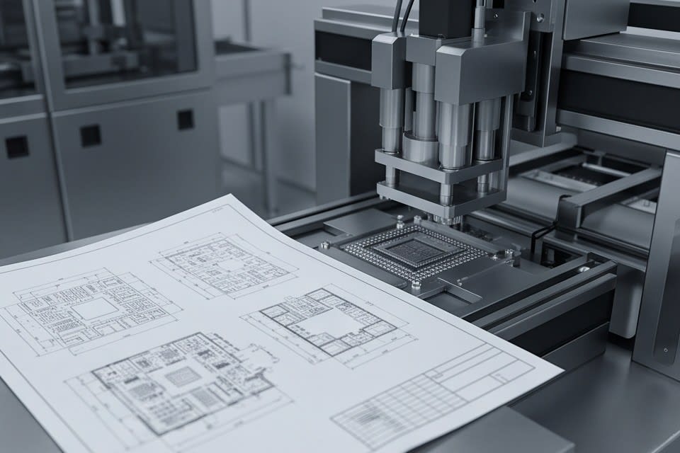
    Planning a custom design while reviewing complex process drawings in front of automation equipment

    When reviewing custom automation equipment for the first time, it may feel difficult not because there are too many options, but because it is hard to clearly understand what your process actually needs. Whether it is a Laminator, Cleaner, or PKG Grinder, what matters first is not the equipment itself, but what role that equipment plays at which point in your process. The more specifically you examine the conditions of your process, the clearer the right equipment becomes.


    Huvics is an advanced technology company that develops and manufactures automation equipment and
    production systems across the semiconductor, LED, Mobile, and Cosmetic industries.
    With top talent and continuous technological innovation, we support customers in improving productivity and
    securing quality competitiveness.

    Huvics Contact

    Phone: 031-374-8285
    Email: cdpark@huvics.com

    Huvics Inquiry

  • Why Flatness Control Matters in Chip Stacking Processes and the Role of Grinding

    Why Flatness Control Matters in Chip Stacking Processes and the Role of Grinding

    Fine integrated structure of a semiconductor wafer seated on a fixture

    According to an analysis by Yole Group, a semiconductor packaging market research firm, the advanced packaging market is expected to grow by more than 10% annually through 2027, with the share of products adopting chip stacking structures expanding rapidly. As stacking chips in multiple layers becomes a core method for achieving higher performance, thickness uniformity and surface flatness between each layer are emerging as the most sensitive variables determining product reliability. What this figure shows is not simply market growth. It reflects the reality that as stacking structures become more complex, the process costs and yield losses caused by failed flatness control increase as well.

    High performance semiconductor chip structure precisely stacked vertically in layers

    Why flatness is critical in the chip stacking process

    In the process of stacking chips layer by layer, flatness is not merely an external appearance standard. Flatness, as defined by SEMI M1, an international semiconductor standards organization, numerically represents how much a wafer surface deviates from an ideal reference plane. In processes below 10 nanometers, total thickness variation (TTV, Total Thickness Variation) must be maintained below 1 micrometer, and the moment this standard is exceeded, the entire subsequent bonding process becomes unstable.

    The issue lies in the stacking structure itself. Thickness variation in the temporary bonding layer between chips determines the lower limit of grinding uniformity, and the nonuniformity that occurs in that layer is directly transferred to the next process step. A deviation created in just one layer can expand into alignment error across the entire stacked structure. This becomes even more pronounced in products such as AI semiconductors and high performance memory, where dozens of chips must be stacked. As the number of stacked layers increases, the speed at which initial flatness deviations accumulate also accelerates.

    In production sites, flatness defects usually become an issue after the grinding process, when subsequent processes are already underway. This creates a structure in which losses increase the later defects are detected.

    Diamond wheel grinding process that uniformly processes the surface of a semiconductor wafer

    Technical design of the PKG Grinder and its response to flatness requirements

    The PKG Grinder addresses this issue at the equipment design level. To secure flatness in the grinding process, two conditions must be satisfied at the same time.

    • The precision of the stage that holds the package firmly so it does not move during processing
    • The cutting precision of the diamond wheel that uniformly removes the surface

    The PKG Grinder combines a high precision stage with a diamond wheel to achieve micron-level thickness control. Whether the package type is FCBGA, WLCSP, QFN·DFN, or solar cell, the core role of this equipment is to process it uniformly to the target thickness required by the customer. No matter what package is handled, the standard is the same. It must be ground without deviation until the target thickness is reached.

    Depending on the production line configuration, users can choose from Full Auto (Type A·Type B) and Manual Type, enabling line design that considers both the level of automation and process flexibility. The design direction of this equipment is to improve yield by stably maintaining processing quality even under high speed process conditions. Ultimately, flatness control depends on how consistently and precisely grinding equipment handles the surface with controlled force and accurate motion paths.

    Precision inspection that checks wafer surface condition using a laser after the grinding process

    Quality control extending to post grinding processes

    Flatness control is not complete simply because grinding has ended. After grinding, the surface condition must be inspected precisely, and the detection limit of modern inspection systems using laser scattering is approximately 20 to 30 nanometers. However, actual sensitivity varies greatly depending on the wafer surface condition. If residual contamination or fine scratches remain on the surface after grinding, the inspection accuracy itself may decline.

    There are also requirements that the contact surface roughness of packaging substrates must be controlled below 20 nanometers, and further below 5 nanometers, to form fine wiring. To reliably secure this level of surface quality, the precision of the cleaning process after grinding is also important. If the connection between grinding and cleaning is broken, it becomes difficult to guarantee precision at the inspection stage.

    As demand for AI semiconductors and high performance memory increases, the number of stacked layers and package complexity continue to rise. In a trend where required flatness standards and surface quality standards are becoming stricter at the same time, an integrated approach that covers the entire process is becoming increasingly important, beyond the performance of grinding equipment alone.

    Automated semiconductor production line that enables precise quality control and process efficiency

    The growth figure for the advanced packaging market mentioned in the first sentence ultimately leads to one question. In a situation where more chips must be stacked more thinly, how can flatness be maintained consistently. Only when the entire process, starting with the precision of grinding equipment and continuing through cleaning and inspection, is aligned to a single standard can the reliability of stacked structures be secured. In the chip stacking process, flatness control is not an issue of a single piece of equipment, but an issue of overall process design.


    Huvics is an advanced technology company that develops and manufactures automation equipment and
    production systems across the semiconductor, LED, Mobile, and Cosmetic industries.
    With outstanding talent and continuous technological innovation, we support customers in improving productivity and
    securing quality competitiveness.

    Huvics Contact

    Phone: 031-374-8285
    Email: cdpark@huvics.com

    Huvics Inquiry

  • AI Semiconductor Packaging Yield: How to Improve It Step by Step from Grinding to Cleaning

    AI Semiconductor Packaging Yield: How to Improve It Step by Step from Grinding to Cleaning

    A semiconductor packaging process site where multiple pieces of equipment are organically connected

    When I first looked closely at a semiconductor packaging site, there was one question customers commonly asked. “The grinding went well, so why do defects keep appearing during bonding?” That question once again confirmed that the root of the problem is not a single piece of equipment, but the entire flow of the process. At that site, I learned firsthand that even a slight deviation in flatness can affect every layer built on top of it.

    A semiconductor stacked structure with dozens of dies precisely stacked vertically

    Why flatness is critical in AI semiconductor packaging

    HBM(High Bandwidth Memory), now a core component of artificial intelligence semiconductors, is built by vertically stacking dozens of thin dies. In a 12 layer stack, each die is about 50 micrometers thick, but when the stack increases to 16 layers, the die must be thinned to about 30 micrometers. As the die becomes thinner, the rigidity of the wafer itself decreases, and the risk of warpage and cracking during the process increases as well.

    Variation in surface flatness is not simply a dimensional issue. According to a technical report from Applied Materials, even minute surface variations directly affect bonding quality and yield. As the number of stacked layers increases, the requirements for thickness uniformity in each layer become stricter, and tolerances become narrower. As package types such as FCBGA, WLCSP, and QFN become more diverse, these requirements become even more complex. Ultimately, flatness control in the packaging process is not optional. It is a variable that determines yield itself.

    A process scene in which a wafer surface is finely ground using a diamond wheel

    How the grinding process determines flatness

    The grinding process is a key step that determines the thickness and surface flatness of semiconductor dies. Unlike general cutting processes, precision grinding uses a diamond wheel to remove material in micron units while achieving the desired thickness and flatness at the same time. The tolerance achievable through precision grinding is around ±0.001~0.005mm, and surface roughness reaches Ra 0.2~0.8μm. This is 5~10 times more precise than general CNC milling.

    These figures matter not simply because they show how precise the process is, but because that precision directly determines the bonding quality of the subsequent bonding process. Grinding equipment that combines a high precision stage with a diamond wheel must be able to maintain thickness uniformity even in high speed processing. It is also important to have a configuration that allows flexible selection between fully automatic and manual types depending on the nature of the production line. Huvics PKG Grinder is designed to uniformly process various package types such as FCBGA, WLCSP, and QFN down to the thickness required by the customer. Choosing a grinding machine also means deciding the precision level for the entire process.

    A process of washing the die surface immediately after grinding by spraying cleaning liquid through a precision nozzle

    Why cleaning after grinding must be treated as one integrated step

    The die surface after grinding is in its most vulnerable state during the process. If fine particles and residues generated during grinding remain on the surface, they can lead to bonding defects in subsequent bonding or packaging steps.

    According to technical data from MSP/TSI, particle removal efficiency in the cleaning process is determined by multiple factors such as cleaning time, temperature, chemical concentration, and agitation method. How precisely these variables are controlled determines final quality. Simply rinsing with water makes it difficult to effectively remove residual particles at the submicron level.

    Huvics cleaning system uses a multi stage method that combines micro bubbles, water jets, and an air knife to remove surface contamination particles step by step, and its oven drying function handles residual moisture after cleaning. When analyzing the process of a customer who came with a camera module defect rate issue, repeated residual particles were occurring because the agitation conditions in the cleaning step had not been optimized. In semiconductor tray cleaning as well, the key was to design different cleaning conditions according to complex contamination types. This is exactly why how a surface precisely processed by grinding is finished in the cleaning step can completely change the value of the process.

    Automated semiconductor process equipment organically connected along a conveyor belt

    The precision of the stacked structure required by AI semiconductors cannot be completed by the performance of grinding equipment alone. Only when cleaning can fully preserve the flatness created by grinding do those numbers truly have meaning. The two processes must be designed as one continuous flow. That is the real standard that determines packaging quality.


    Huvics is an advanced technology company that develops and manufactures automation equipment and
    production systems across the semiconductor, LED, Mobile, and Cosmetic industries.
    With top talent and continuous technological innovation, we support customers in improving productivity and
    securing quality competitiveness.

    Huvics Contact

    Phone: 031-374-8285
    Email: cdpark@huvics.com

    Huvics Inquiry

  • Why Semiconductor Packaging Reliability Must Be Managed Step by Step from Grinding to Cleaning

    Why Semiconductor Packaging Reliability Must Be Managed Step by Step from Grinding to Cleaning

    Cross sectional structure of high performance semiconductor chips stacked vertically in multiple layers

    It is time to move beyond the idea that shaving a few more micrometers off the thickness of a semiconductor package will not change its performance. As demand for AI semiconductors and high performance memory grows explosively, stacked packaging that vertically stacks dozens of chips has become common, and a single thickness variation has become a factor that can shake the reliability of the entire process. This may sound exaggerated, but when you examine the defect data accumulated in actual manufacturing sites, it is far from an empty claim. Let us take a closer look at how equipment operation becomes the starting point of quality.

    Measurement equipment precisely inspecting semiconductor wafer thickness variation and uniformity

    Why Thickness Uniformity Determines Packaging Reliability

    In high performance semiconductor packaging, thickness uniformity is not optional. In a structure where chips are stacked in multiple layers, even a slight deviation in the thickness of each layer can create voids at the joints or concentrate stress at specific points during subsequent bonding or stacking processes. This phenomenon is not easily noticeable at first, but over time it seriously reduces electrical reliability.

    The concept of total thickness variation, or TTV, reveals this issue numerically. This is why international standards define the allowable TTV range for advanced applications at ±2 to 5 micrometers. As package types become more diverse, such as FCBGA, WLCSP, and QFN, the required machining precision becomes even higher. On manufacturing sites, allowable deviations vary by package type, and process conditions are adjusted in detail. Ultimately, the stability of the packaging process depends on how uniformly thickness can be maintained.

    Grinding equipment processing wafer thickness in micrometer level control

    How Grinding Equipment Operation Determines TTV Stability

    The way grinding equipment achieves TTV stability lies in the combination of mechanical precision and process design. Spindle speed, the material and grit size of the grinding wheel, and the leveling precision of the stage must work together to enable uniform machining at the micrometer level. In the industry, grinding equipment spindles are known to operate in the range of 5,000 to 60,000 RPM depending on the application and material, and selecting the appropriate speed within this range directly affects yield.

    Huvics PKG Grinder combines a high precision stage with a diamond wheel to deliver stable grinding within this range. With Full Auto A Type, B Type, and Manual Type options, line configurations can be selected flexibly, allowing the process to be designed differently according to production scale or product characteristics. The level of automation selected affects the production efficiency of the entire line, and reducing operator intervention also reduces sources of variation. Controlling TTV within specification at the grinding stage is how the foundation is prepared for all subsequent processes.

    Cleaning process spraying liquid onto the wafer surface to remove fine residues

    Why the Cleaning Process Is the Final Gateway to Packaging Quality

    Even after grinding is completed, the risk factors in the packaging process do not disappear. If fine particles and machining residues generated during grinding remain on the surface, they can lead to bonding defects or contamination in later processes. Particle Removal Efficiency, or PRE, is an indicator of how effectively a cleaning system removes surface contaminants. As device structures become finer, even very small particles can affect performance, making it increasingly important to achieve high PRE.

    In the post grinding cleaning process, it has been confirmed that controlling the pressure of the buffing disk and the flow rate of chemical solutions is effective in improving PRE. Huvics Cleaner System adopts a multi step cleaning method that sequentially applies micro bubbles, water jet, and air knife, and adjusts cleaning conditions according to products with various forms and materials, including camera modules, sensors, VCM motors, and trays. It also includes an Oven Dry function, enabling the process from cleaning to drying to be handled in one continuous flow. Managing the connected process from grinding to cleaning and drying in an integrated way, rather than separating each step, is becoming a key trend for improving packaging quality stability.

    Semiconductor packages processed with uniform thickness and clean surfaces and aligned on a tray

    Only when grinding precision and cleaning efficiency work together can the reliability of the packaging process truly be secured. Controlling thickness variation at the micrometer level and completely removing contamination particles generated during that process are quality standards for high performance packaging. The fact that the way equipment is operated directly determines the reliability level of the product prompts us to reconsider the standards by which processes should be designed and managed.


    Huvics is an advanced technology company that develops and manufactures automation equipment and
    production systems across the Semiconductor, LED, Mobile, and Cosmetic industries.
    With outstanding talent and continuous technological innovation, we support customers in improving productivity and
    securing quality competitiveness.

    Huvics Contact Information

    Phone: 031-374-8285
    Email: cdpark@huvics.com

    Contact Huvics

  • Thickness Variations That Disrupt Semiconductor Package Yield, Explained Through Grinding and Lamination Field Applications

    Thickness Variations That Disrupt Semiconductor Package Yield, Explained Through Grinding and Lamination Field Applications

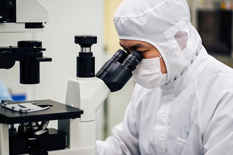
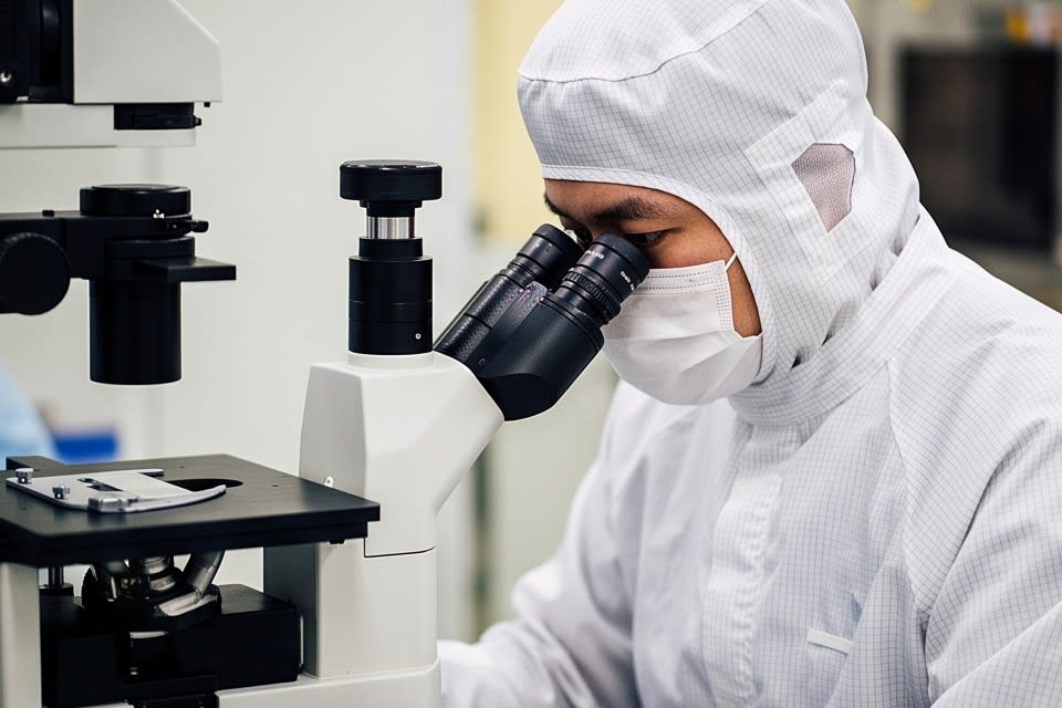
    A semiconductor manufacturing site where an operator inspects micron-level errors under a microscope

    Semiconductor quality management is, in simple terms, a matter of how precisely allowable tolerances are controlled at each stage of the process. Invisible micron-level variations determine the reliability of the finished product, and this issue becomes even more apparent in advanced package structures where chips are stacked in multiple layers. The moment terms such as ‘thickness uniformity’ or ‘flatness’ come up on the manufacturing floor, they are not simply about dimensions but about issues that affect overall yield and reliability.

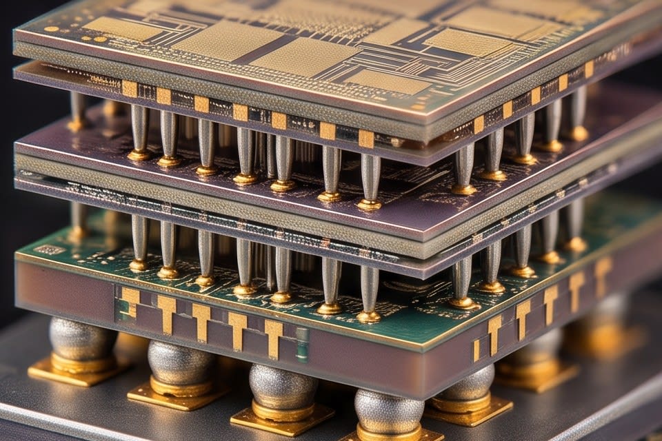
    Cross-sectional structure of an advanced semiconductor package with vertically stacked dies

    Why Thickness Variation Undermines Package Reliability

    Stacking chips also means, in a sense, stacking tolerances. In structures such as AI semiconductors or high-performance memory, where dozens of dies are vertically stacked, thickness variation in each layer accumulates and compromises the flatness of the entire package.

    The international semiconductor standard JEDEC defines the maximum allowable warpage for large flip chip packages as 200μm, and cases have been reported where warpage deformation reaches 87μm under reflow temperature conditions. Once this value exceeds the threshold, signal integrity becomes unstable and interlayer bonding defects can occur.

    In high-bandwidth memory, it is already widely recognized across the industry that thickness variation alone in the interposer manufacturing process can cause impedance deviation. If thickness is not uniform, electrical performance cannot be uniform either, and the principle that an uneven package cannot be reliable has become the starting point of advanced package design.

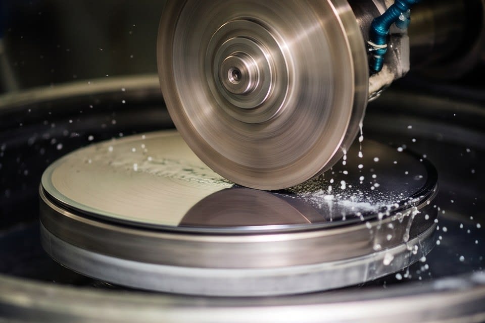
    A process that machines the surface of a semiconductor wafer with a high-speed rotating grinding wheel

    How a Reference Surface Is Created in the Grinding Process

    PKG Grinder is equipment that directly addresses this issue. Regardless of package type, including FCBGA, WLCSP, QFN, DFN, and Solar Cell, it performs micron-level precision grinding to achieve the target thickness required by the customer.

    This machining method, implemented through the combination of a high-precision stage and a diamond wheel, maintains uniform results even in high-speed processes without reducing yield, contrary to the common belief that speed and precision are usually inversely related. Because it supports both Full Auto and Manual configurations, it can respond flexibly to everything from low-volume, high-mix lines to mass production systems.

    Grinding is not simply a task of reducing thickness. It is the process of creating a reference surface on which all subsequent processes depend. Since the uniformity and flatness of that reference surface determine the reliability of the final package, precision control in the grinding stage is the practical key to securing quality.

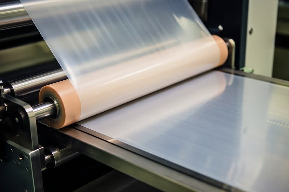
    A semiconductor package film lamination process fed through rollers

    The Impact of the Lamination Process on Adhesion Reliability

    Thickness uniformity issues do not occur only in the grinding process. If film thickness is formed unevenly during the ABF lamination process, the electrical performance of subsequent circuits varies from layer to layer and reliability decreases.

    Lamination may appear to be a simple process of attaching film, but even a slight imbalance in the combination of temperature and pressure can cause delamination defects or uneven adhesion strength. According to research findings, cases have been reported where delamination defects decreased by up to 67% when optimized lamination parameters were applied.

    Huvics’ laminator system features an integrated process structure that connects everything from Expander to UV Curing in a single flow, and secures both adhesion strength and process stability through Lamp and LED type UV curing systems. With Semi Auto and Manual options, it can support various product specifications and production requirements, and it is designed to reduce takt time by simplifying process steps.

    Field applications continue to confirm that overall package quality stability is achieved only when the two processes, setting the reference surface through grinding and building layers through lamination, are each precisely controlled.

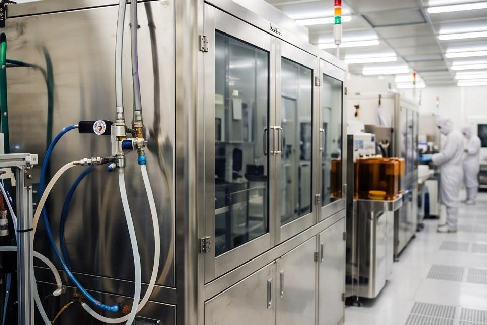
    View of semiconductor manufacturing equipment in a cleanroom where precise process control is performed

    Semiconductor package quality cannot be guaranteed by the completeness of a single process alone. Reliable results emerge only when the uniform reference surface created in the grinding stage works together with precise temperature and pressure control in the lamination stage. Managing micron-level variation is ultimately a matter of designing the entire process as one connected flow, and the essence of quality management lies in how tightly the allowable tolerance of each stage can be narrowed within that flow.


    Huvics is an advanced technology company that develops and manufactures automation equipment and
    production systems across the semiconductor, LED, Mobile, and Cosmetic industries.
    With top talent and continuous technological innovation, we support customers in improving productivity and
    securing quality competitiveness.

    Huvics Contact

    Phone: 031-374-8285
    Email: cdpark@huvics.com

    Huvics Inquiry

  • Precision Grinding and Multistage Cleaning Core Principles That Determine Stacked Packaging Reliability

    Precision Grinding and Multistage Cleaning Core Principles That Determine Stacked Packaging Reliability

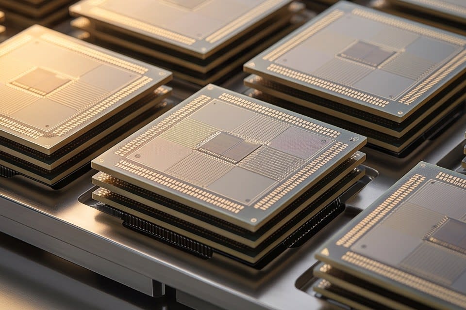
    View of multilayer stacked semiconductor packages arranged in rows

    Just a few years ago, thickness control in semiconductor packages was measured by whether they were thin enough. But as AI semiconductors and high-performance memory have become mainstream, the more important question has shifted to how uniform they are. As structures that stack chips in multiple layers have become common, even a single thickness deviation has emerged as a variable that can undermine the reliability of the entire package. As stacked structures become more complex, precision machining and cleaning technologies will become even more decisive standards for process quality.

    View of solder microbumps placed inside a semiconductor package

    Why Thickness Uniformity Is a Key Quality Variable in Stacked Packaging

    In 3D IC packaging structures where chips are stacked vertically, thickness uniformity is not simply a dimensional issue. The solder microbumps that connect the chips between each layer repeatedly contract and expand during thermal cycling, and if there is variation in chip thickness, the stress distribution concentrated on the bumps changes. According to research published on ScienceDirect, thermal cycling tests of 3D IC packaging showed that creep in solder microbumps, plastic deformation caused by high-temperature load, can increase by up to 50%, directly affecting thermomechanical reliability.

    The greater the thickness deviation, the more stress becomes concentrated on specific bumps, and package warpage also worsens. As the number of stacked layers increases, the allowable tolerance range for each layer inevitably becomes narrower. When thickness nonuniformity in a single chip accumulates, the flatness of the entire package collapses, leading to bonding defects or electrical shorts in subsequent processes. In the end, thickness variation may not be visible, but it appears directly in the reliability metrics of the final product. As stacked packaging advances, securing thickness uniformity is becoming the starting point of process quality.

    View of a wafer or chip thickness being precisely machined using a diamond wheel

    Limitations of Conventional Machining Methods and the Role of Precision Grinding Technology

    Conventional grinding and chemical mechanical polishing have long been used as standards in semiconductor thinning processes, but their limitations are clear at the level of precision required by advanced packaging. According to an analysis by Eureka PatSnap, conventional grinding and chemical mechanical polishing processes often exceed thickness deviations of ±2μm, falling short of the latest package specifications that require submicron precision. As package types become more diverse, such as FCBGA, WLCSP, and QFN·DFN, and target thickness values vary, it is difficult for a single method to handle all specifications with the same level of precision.

    The moment deviation exceeds ±2μm, the package fails to meet the flatness criteria required in the next process, directly leading to yield loss. Micron-level grinding that combines a high-precision stage with a diamond wheel is one approach to closing this gap, and the same analysis shows that it can reduce material waste by 15 to 30% compared with conventional methods. Equipment such as a PKG Grinder, which supports both fully automatic and manual configurations, is designed to secure stable thickness precision in high-speed processes while maintaining production line flexibility. More important than which method is chosen is first defining the target package specification and allowable tolerance, then selecting the machining method that fits them.

    View of fine water droplets formed on the surface of a semiconductor chip

    How the Cleaning Process Determines Final Quality

    If precision machining reduces thickness variation, the cleaning process determines the surface condition before the result moves on to the next stage. For components that require ultra-precision optical and electrical characteristics, such as camera modules or autonomous driving sensors, even a single fine particle left after grinding can result in a defect judgment. In the field, cleaning is often regarded as the last step, but in practice it is the process that determines final quality.

    According to research published in MDPI, cleaning solutions containing micro-nano bubbles improve the photoresist removal rate by 30%. A multistage cleaning method that applies Micro Bubble, Water Jet, and Air Knife step by step is structured to separate and discharge contaminant particles at each stage that are difficult to remove with a single method. For parts with complex shapes, such as VCM motors or semiconductor trays, the combination and sequence design of cleaning methods directly affect removal efficiency. When residual moisture is also removed through the Oven Dry process after cleaning, the possibility of secondary contamination in subsequent assembly or inspection processes is reduced.

    Lower defect rates and stable yield ultimately come from how precisely the surface is controlled at this cleaning stage. The fact that invisible particles determine the quality of the entire process becomes clear the moment cleaning results are connected to shipping quality.

    View of cleaned semiconductor components aligned and loaded on trays

    Reducing defects in semiconductor processes is not a matter of just one step. Package reliability is secured only when two processes work together: precision grinding that controls thickness variation at the micron level, and multistage cleaning that removes surface contaminant particles step by step. In a structure where the precision of each individual process determines the yield and reliability of the final product, which technologies are selected and how they are combined become practical benchmarks of manufacturing competitiveness.


    Huvics is an advanced technology company that develops and manufactures automation equipment and
    production systems across the semiconductor, LED, Mobile, and Cosmetic industries.
    With top talent and continuous technological innovation, we help customers improve productivity and
    secure quality competitiveness.

    Huvics Contact

    Tel: 031-374-8285
    Email: cdpark@huvics.com

    Huvics Inquiry

  • What are the 3 design criteria that improve laminator process stability?

    What are the 3 design criteria that improve laminator process stability?

    A close-up view of tape attachment showing the importance of the lamination process

    In the semiconductor process, many people still overlook the fact that a single sheet of tape can determine yield. Even a slight deviation in the precision of the lamination process can lead to defects across an entire wafer, and the resulting loss goes far beyond simple rework costs. The quality of the process depends on how accurately the direction of equipment design reflects the needs of the production site.

    A precise process in which metal rollers closely attach tape to a wafer

    Process principles and configuration of a laminator system

    In the semiconductor packaging process, a laminator handles a sequence of operations that attaches tape to a wafer, controls the adhesion state through UV curing, and then separates the tape after dicing or backgrinding. The reason this process may look simple is that the visible movement is concise, but in reality, micron-level alignment and the maintenance of uniform adhesion are required at the same time.

    UV curing adhesives lose adhesion and harden when exposed to ultraviolet light, and this principle makes it possible to separate chips after dicing without damage. A one-stop configuration that evenly expands the tape with an Expander, precisely attaches it to the wafer with a Tape Mounter, and controls the adhesion state through UV Curing is integrated within a single laminator system.

    Overall process stability is secured only when each stage does not operate independently but is connected as a continuous flow. If adhesion uniformity breaks down, chip breakage occurs in the subsequent dicing process, and if the UV curing time is inaccurate, separation defects follow. The core premise of a laminator system is that the process must be designed not as a structure where errors accumulate, but as a method that blocks errors at each stage. The process of attaching, curing, and separating tape is implemented as a continuous sequence of precise control.

    A UV LED curing module that prevents thermal damage while performing a process on a wafer

    The shift in UV curing methods began with on-site inconvenience

    The change in selection criteria for UV curing methods at production sites began not with advances in equipment technology, but with practical inconvenience in the field. Conventional mercury lamp methods require warm-up time before operation and a cooldown process after operation, which often interrupts process flow. Because they generate a large amount of infrared heat, they pose a risk of thermal damage to heat-sensitive thin-film substrates or electronic components, and this was a variable that on-site engineers had to account for whenever setting process conditions.

    The UV LED method starts irradiation immediately when powered on and stops the moment it is turned off, so no warm-up or cooldown is required. As a cold light source, it does not apply heat to the substrate, allowing stable application even to sensitive materials, and according to data from Noble Light, UV LED consumes 30~70% less energy than mercury lamps. In dicing and backgrinding processes, tape adhesion must be reduced quickly to shorten cycle time, and UV LED cold light technology efficiently supports this process.

    The Huvics laminator system is configured so that both Lamp and LED methods can be selected, allowing flexible responses according to customer material characteristics and process conditions. Semi Auto and Manual options are also provided, making application possible even on lines with different production scales or automation levels. In a position where mercury lamps were once used as a matter of course, selection criteria have changed as on-site conditions have changed.

    An overall view of a laminator system integrated into a single framework from tape attachment to curing

    Customer feedback from the field changed laminator design

    When Huvics designs a laminator system, the first reference point is the problems that actually occur at customer sites. In cases where defects repeatedly occurred in the semiconductor tape bonding process, uneven tape attachment pressure and variations in UV curing time were acting in combination. Replacing a single piece of process equipment alone did not solve the problem, and the approach shifted toward restructuring the entire process from Expander to UV Curing as one continuous flow.

    When processes are integrated, contamination and alignment errors that occur during transfer between equipment are reduced, and Tact Time is also shortened. In the wafer lamination process, UV curing can be completed within a few seconds depending on the adhesive type, and when this time is accurately reflected in process design, unnecessary waiting disappears from the overall cycle. To secure both adhesion strength and process stability, curing conditions must remain consistent in every cycle, and the control of irradiation time and illuminance for this purpose becomes a key variable in equipment design.

    When customer requirements lead not simply to a specification request but to a redesign of the entire process, the data and know-how gained through that process become the foundation for the next equipment development. Cases in which feedback from the field has substantially changed the structure and options of laminator systems have been steadily accumulated.

    The interior of a semiconductor cleanroom where automation equipment is arranged according to process flow

    Equipment specifications can be checked in a catalog, but the problems those specifications were designed to solve can only be understood in the field. The fact that the laminator system is integrated as one flow from Expander to UV Curing, and the fact that customers can choose between UV Lamp and LED, are the result of specific inconveniences and requirements from customer sites changing the direction of design. The evolution of a process begins not with the technology itself, but with how accurately the context in which that technology is used is understood.


    Huvics is an advanced technology company that develops and manufactures automation equipment and
    production systems across the semiconductor, LED, Mobile, and Cosmetic industries.
    With top-tier talent and continuous technological innovation, we support customers in improving productivity and
    strengthening quality competitiveness.

    Huvics Contact

    Phone: 031-374-8285
    Email: cdpark@huvics.com

    Huvics Inquiry

  • Key Criteria for Building Automated Equipment to Reduce Semiconductor Process Defects

    Key Criteria for Building Automated Equipment to Reduce Semiconductor Process Defects

    Semiconductor wafer circuit pattern with a precise micron-scale structure

    In the past, the hands and eyes of skilled operators were the key variables that determined quality on semiconductor manufacturing sites. However, as chip integration has increased and package structures have become more complex, the microscopic errors that occur in processes involving human intervention have emerged as issues that can affect overall yield. As process precision requirements have moved below the micron level, manual-centered production methods have gradually begun to reveal their limits. Within this trend, semiconductor automation equipment is becoming not an option, but the starting point of process design.

    Cleaning liquid being precisely applied to a wafer surface through a spray nozzle

    The Beginning of Process Defects, Automation That Blocks Contaminant Particles

    In semiconductor manufacturing processes, many defects begin with contaminant particles that are invisible to the eye. A single fine particle left on the surface of a wafer or package can cause an electrical short or lead to bonding defects. Research on cleaning processes confirms that the mechanical force generated when a PVA brush contacts the surface can effectively remove particles without cross-contamination, even with low-concentration chemical solutions. In this way, the principle of particle removal is not simply the use of detergent, but a combination of physical force and chemical action.

    Comparative data showing that error rates appear at 1 to 2% or higher in manual work environments, while they drop to around 0.01% on automated lines, clearly demonstrates how significant this difference is. For components with diverse shapes and materials, such as camera modules, sensors, VCM motors, and trays, maintaining consistent cleaning conditions becomes more difficult, and the more often human hands are involved, the more contamination inflow paths increase. When automation equipment is introduced into the process, these variables can be kept within a controlled range. Across advanced manufacturing sites, there is a growing recognition that blocking the starting point of defects is the first condition for yield management.

    Automation line equipment arranged at regular intervals in a semiconductor manufacturing site

    How Should the Level of Automation Be Judged for Each Process

    Introducing automation equipment does not mean the same method can be applied to every process. Cleaning, lamination, and grinding each require different levels of automation and equipment configurations. A full-auto line can achieve a production speed about twice as fast as a semi-auto line, but it requires large initial capital investment and precise system tuning as a prerequisite. In contrast, the semi-auto method has a lower initial cost burden, but requires continuous manpower input and a separate management system to maintain consistency between processes.

    In the cleaning process, a multi-stage method combining Micro Bubble·Water Jet·Air Knife offers higher surface contaminant removal efficiency than a single cleaning method, and when the Oven Dry function is added, the drying process can also be completed in one continuous flow. In the lamination process, equipment configured as a one-stop flow from Expander to UV Curing is advantageous for reducing process steps and shortening takt time. The Cleaner System and Laminator System from Huvics support both Full Auto and Manual options, and are designed to be configured flexibly according to the scale of the production line and product characteristics.

    Choosing full auto based only on production speed, or remaining with semi auto based only on cost, can disrupt the balance of the entire process. The key to equipment implementation is to first establish the criteria for deciding what level of automation should be applied to each process.

    Automation equipment attaching film to a wafer surface or transferring it with precision

    The Moment Yield Changes, Combining Process Design and Equipment

    The effect of automation equipment becomes clearest when it is verified through numbers. According to semiconductor cleaning process research published on ResearchGate, there was a reported case in which process improvement reduced the defect rate from 20% to 5%. This figure shows that changing even one cleaning process can create a meaningful change in yield.

    Huvics has a track record of analyzing chronic defect issues that occurred in semiconductor tape bonding processes and resolving them by redesigning the overall process flow. In camera module processes as well, there have been cases where defect rates were reduced by precisely adjusting cleaning conditions, and this was not simply the result of replacing equipment, but of examining the process structure itself.

    However, defects do not automatically disappear simply by introducing automation equipment. If you do not review together where contamination occurs in the process, whether the cleaning conditions match product characteristics, and whether there are residual issues after drying, the effect of equipment investment may be reduced. This confirms that automation equipment becomes a practical tool for reducing process defects when equipment selection, process design, and adjustments based on on-site data are carried out together.

    Interior view of a cleanroom with multiple enclosed automation systems arranged in rows

    As semiconductor manufacturing environments become more complex, reducing process defects is no longer simply a matter of selecting good equipment. Yield begins to change only when you evaluate together where contamination starts in the process, how far the level of automation should be raised, and whether the equipment fits actual production conditions. Whether the process is cleaning, lamination, or grinding, when the starting point is the fact that each process requires a different level of precision and automation method, equipment implementation becomes an investment rather than a cost.


    Huvics is an advanced technology company that develops and manufactures automation equipment and
    production systems across the Semiconductor, LED, Mobile, and Cosmetic industries.
    With top talent and continuous technological innovation, we support customers in improving productivity and
    securing quality competitiveness.

    Huvics Contact

    Tel: 031-374-8285
    Email: cdpark@huvics.com
    Huvics Inquiry

  • What Standards Protect Yield in Semiconductor Cleaning and Lamination Processes?

    What Standards Protect Yield in Semiconductor Cleaning and Lamination Processes?

    Surface of a semiconductor wafer engraved with fine circuit patterns on the micrometer scale

    Cleaning is not the final step of the process. In many production sites, cleaning is often seen as a step that simply wipes things down once at the end, but actual yield data points in the opposite direction. In semiconductor manufacturing, a single contaminant particle only a few micrometers in size left on the surface can disrupt the entire downstream process, and this fact makes the cleaning process not merely a matter of maintaining cleanliness, but the starting point of a quality strategy.

    Close-up of a semiconductor wafer surface with fine patterns precisely engraved in a grid structure

    Why the Cleaning Process Determines Yield

    The cleaning process accounts for a much larger share of semiconductor manufacturing than many expect. According to MDPI Nanomaterials, the cleaning process takes up about 30% of total production time, and related costs exceed 20% of the overall budget. This does not simply mean it is a time-consuming process. It means cleaning is deeply connected to the overall process flow and quality.

    Surface contaminant particles cannot be identified with the naked eye, but they appear as defects in later adhesion, curing, and packaging stages. For this reason, how particles are removed during the cleaning stage effectively determines the final yield.

    This is also why microbubbles, or ultrafine bubbles, are attracting attention. When microbubbles collapse, the shock waves and localized high-temperature and high-pressure effects physically separate contaminant particles adhered to the surface. When water jets, or high-pressure water streams, and air knives, or high-speed air flows, are combined in stages, particle removal efficiency increases significantly compared to a single method. By integrating the oven drying process as well, secondary contamination paths caused by residual moisture after cleaning can also be blocked.

    In this way, the industry is increasingly recognizing that cleaning is not an act of wiping, but a matter of process design that blocks contamination paths step by step.

    UV LED irradiation equipment that stably cures film after the lamination process

    The Meaning of Curing Methods in the Lamination Process

    In the lamination, or film attachment, process as well, the key quality variable is shifting from how the film is attached to how accurately and how stably it is cured. In the UV curing step that follows tape mounting, or the attachment of tape for fixing semiconductor chips, the choice of light source is not simply a matter of equipment specifications.

    Conventional mercury lamp systems require about 15 minutes of warm-up and cool-down cycles before lighting, and they continuously consume power regardless of whether irradiation is being performed. In contrast, UV LED systems can be turned on immediately and use energy only during operation. Energy consumption is reduced by more than 80% compared to mercury lamps, and service life reaches up to 20,000~30,000 hours compared to about 1,000 hours for mercury lamps. A longer replacement cycle reduces the frequency of line stoppages and also lowers maintenance costs.

    The Huvics laminator system integrates everything from the expander, or film expansion device, to the tape mounter and UV curing into a single flow, reducing transfer errors and unnecessary waiting time between process stages. Simplifying the process also means blocking, one by one, the paths where defects can occur. Ultimately, how the curing method and integrated process design are selected in the lamination process becomes the basis for determining the operating rate and yield of the entire line.

    Semiconductor trays neatly stacked, where contaminant control is critical

    How to Solve On-Site Challenges: Read the Process First

    On-site challenges are not found in standard catalogs. Take the semiconductor tray cleaning process as an example. Tray materials and shapes, types of contaminants, and drying conditions after cleaning vary by customer. Even when the same cleaning equipment is introduced, if the process parameters are not set correctly, surface damage or residual contamination may occur instead.

    The same applies to camera module defect rates. Fine particles generated during the lens assembly process often cannot be removed under general cleaning conditions, and increasing cleaning intensity creates a dilemma because it can cause physical damage to the module itself.

    Huvics first analyzes the overall manufacturing process of the customer, identifies contamination paths and product characteristics, and then designs the equipment. Reading the process comes before building the equipment. Whether a fully automated, or full-auto, configuration or a manual method is suitable for the line is also determined during this analysis process, and close technical support continues even after equipment delivery.

    Whether it is cleaning, lamination, or grinding, what these cases show is that protecting the basic cleanliness of a process ultimately comes down to how deeply the process is understood.

    Production site scene where workers operate precision equipment and inspect products inside a cleanroom

    Protecting the fundamentals of a process is the hardest task. Cleaning, lamination, precision grinding — these processes may not carry flashy names, but if these steps become unstable, no advanced technology that follows can perform properly. In semiconductor manufacturing sites, basic cleanliness does not simply mean making things clean. It means the ability to accurately identify the different contamination paths in each process and block them with the right method. That ability protects yield, stabilizes the line, and ultimately determines product reliability.


    Huvics is an advanced technology company that develops and manufactures automation equipment and
    production systems across the semiconductor, LED, mobile, and cosmetics industries.
    With top talent and continuous technological innovation, we support improvements in customer productivity and
    the securing of quality competitiveness.

    Huvics Contact

    Phone: 031-374-8285
    Email: cdpark@huvics.com
    Huvics Inquiry