Tag: Semiconductor

  • Why Grinding and Cleaning Process Design Learned from Camera Module and Sensor Production Lines Changes Yield

    Why Grinding and Cleaning Process Design Learned from Camera Module and Sensor Production Lines Changes Yield

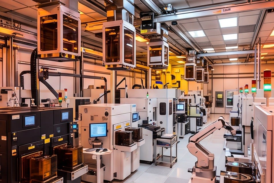
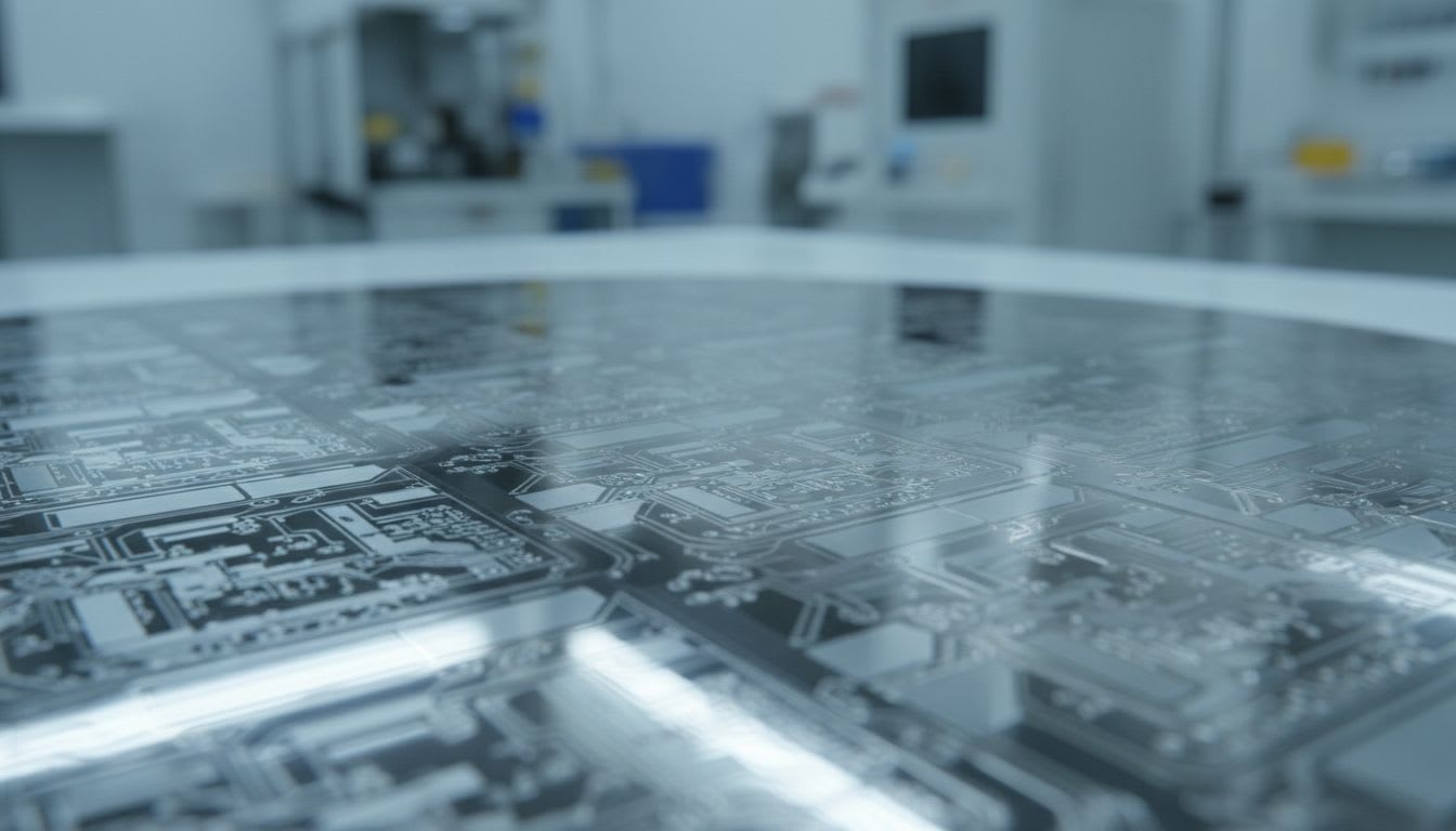
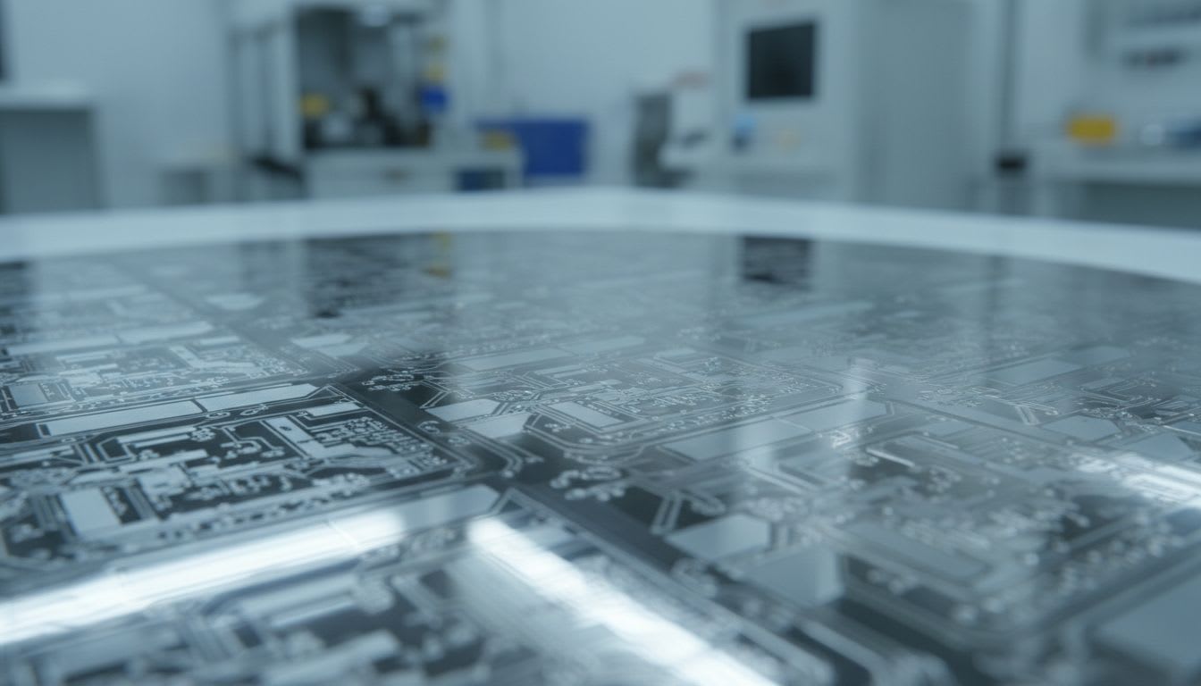
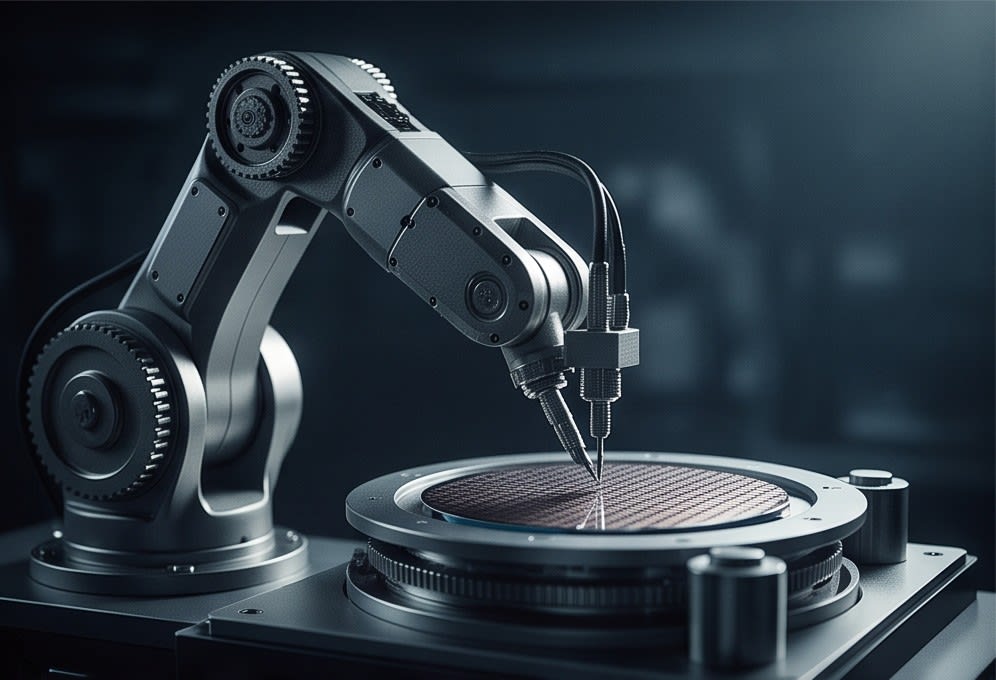
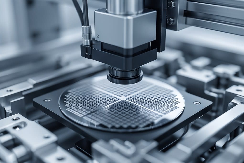
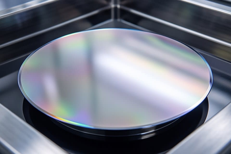
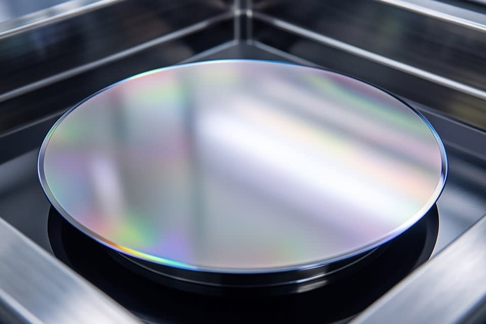
    The glossy and reflective surface of a semiconductor wafer placed on high-precision equipment.

    If you discover too late that a thickness deviation of only a few micrometers has occurred during the grinding process, yield loss and rework costs in downstream processes may already have accumulated. Thickness nonuniformity undermines the reliability of the entire chip stacking structure, and once the package is completed, it can lead to defects that are difficult to reverse. If this issue is left unaddressed, it can spread to delivery delays and customer claims, making precise thickness control essential from the very beginning of the process.
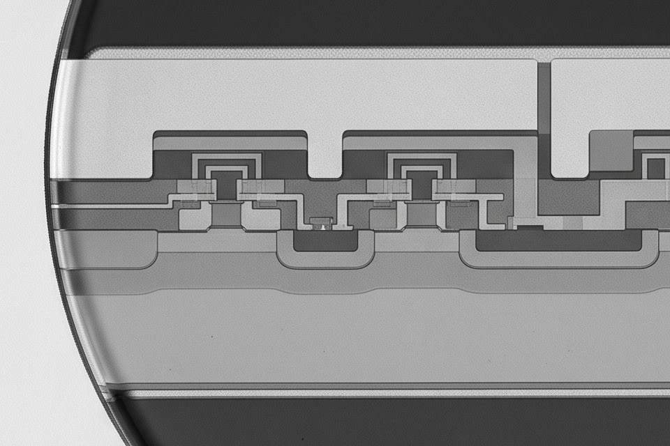
    A fine stacked structure of vertically layered semiconductor chips and a cross section of the internal circuits.

    Why Thickness Uniformity Matters in Chip Stacking Packaging

    As semiconductor packaging technology evolves into 3D stacked structures, maintaining uniform thickness in each chip has emerged as a key factor that determines overall package performance. In structures where multiple chips are stacked vertically, such as high-bandwidth memory, narrower gaps between chips improve signal transmission quality. However, even a slight thickness deviation increases the risk of bonding defects and warpage.

    Across the industry, advanced stacked packaging is moving toward wafer thickness targets in the range of 25 to 50 micrometers. This is less than half the thickness of a human hair, requiring a level of precision that cannot even be verified with the naked eye.

    As package formats become more diverse, including FCBGA, WLCSP, and QFN/DFN, the thickness standards and tolerances required for each structure also vary. This is why target thickness and machining strategies must be set differently depending on the package type, even within the same grinding process. Ultimately, securing thickness uniformity in chip stacking packaging is not simply a matter of machining precision. It has become a process design issue that determines product reliability and overall yield.
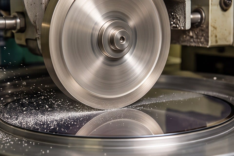
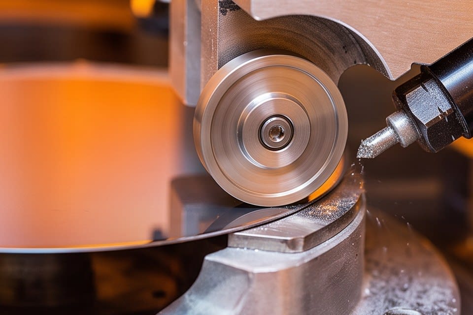
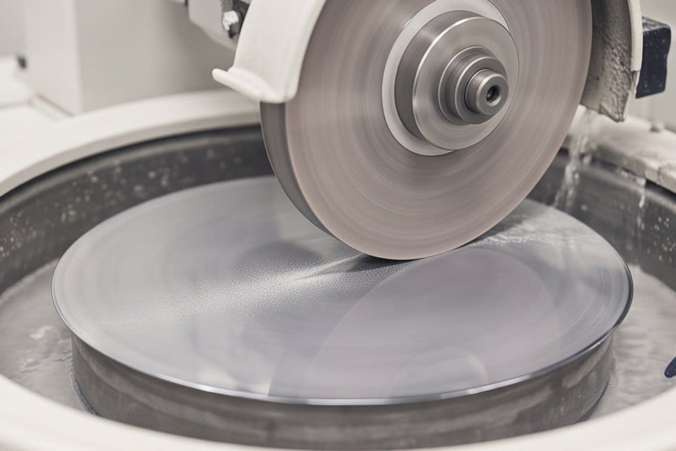
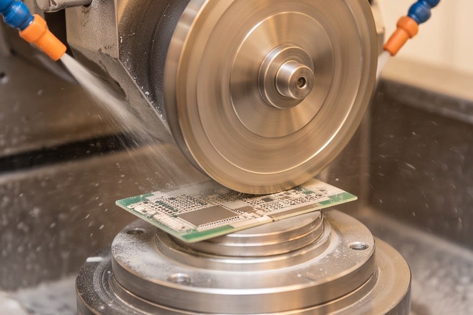
    A machining scene where a diamond wheel grinds the wafer surface and fine particles scatter.

    How the Grinding Process Determines Thickness Uniformity

    The performance of grinding equipment is evaluated mainly by two factors. One is machining precision, and the other is process stability. A grinding method that combines a high-precision stage with a diamond wheel enables thickness control at the micron level and is advantageous for maintaining uniform flatness across the entire wafer surface.

    In WLCSP structures, wafer grinding becomes the core method for reducing the overall package height. In FCBGA structures, the target thickness must be set differently because the package takes advantage of its greater thickness and lower conduction loss. This is why grinding strategies must differ by package type.

    To maintain stable quality even in high-speed process environments, the automation level of the equipment becomes an important variable. The Huvics PKG Grinder supports both Full Auto and Manual configurations, allowing flexible response according to the production line type and required yield. The manual method is suitable for low-volume and high-mix production, while the automated method offers strong advantages in minimizing process variation in mass production environments.

    The key to yield stability lies in which equipment configuration is selected for the grinding process and how precisely the machining conditions are set for each package type.

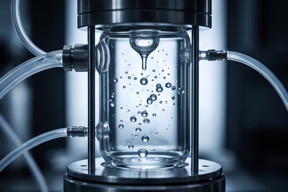
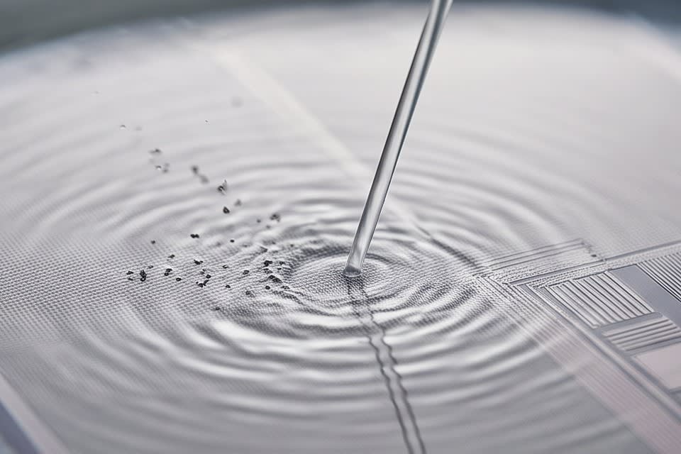
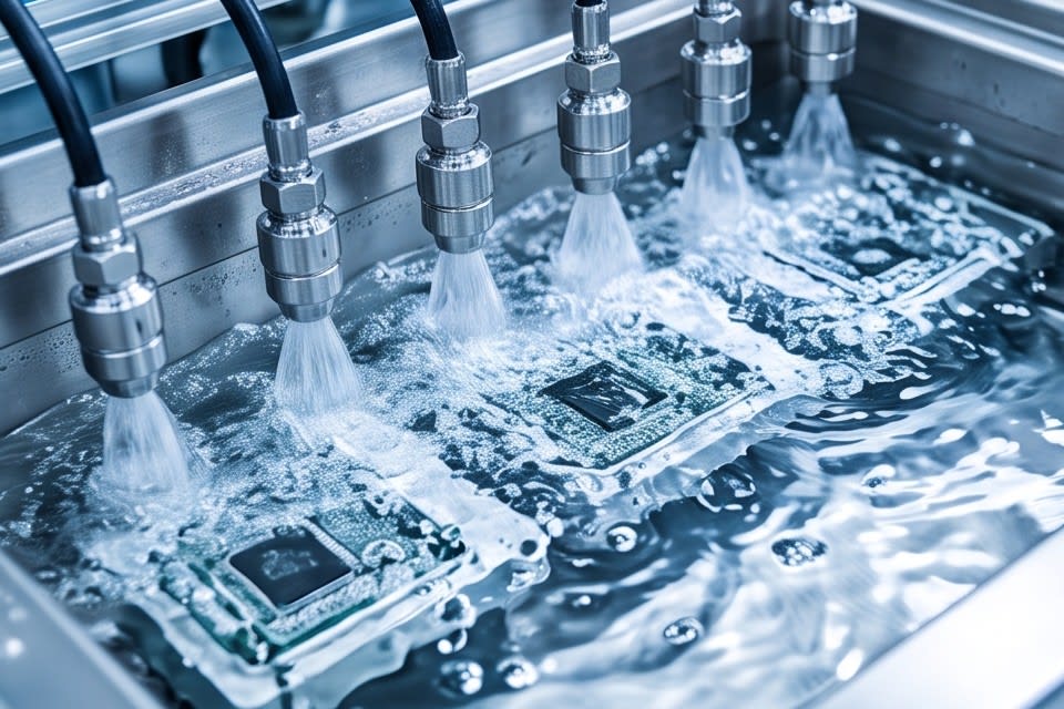
    A cleaning process in which liquid sprayed from a nozzle removes contaminants from the wafer surface.

    Why the Cleaning Process After Grinding Determines Final Quality

    The process is not complete even after grinding is finished. If fine particles and surface contaminants generated during grinding are not removed, they become the source of defects in subsequent processes. In manufacturing sites for ultra-precision components such as camera modules and sensors for autonomous driving, where even a single speck of dust is hard to tolerate, companies repeatedly experience yield collapse the moment the cleaning step is omitted. If contaminant particles remain on the bonding surface, they lead to poor electrical contact, and in optical components, they directly cause image quality degradation.

    A multistage cleaning method that combines microbubbles, water jets, and air knives step by step removes fine contamination on the product surface in different ways at each stage, securing higher particle removal efficiency than a single cleaning method. After cleaning, a drying process must follow to completely remove residual moisture, and equipment integrated with an oven drying function can handle these two steps within one continuous flow.

    Huvics has applied solutions tailored to different contamination conditions and cleaning requirements at each site, including cases involving semiconductor tray cleaning and camera module defect improvement. Since cleaning conditions vary depending on product type and process environment, reviewing both equipment flexibility and site suitability leads to practical quality improvement.
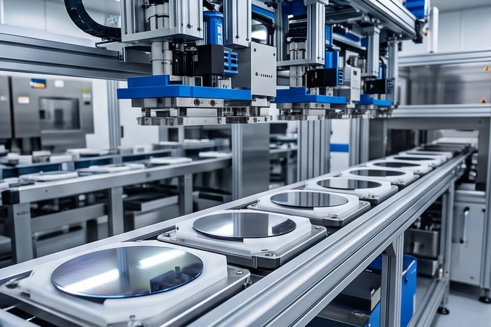
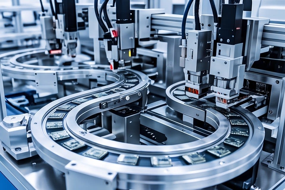
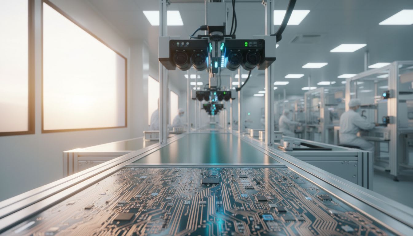
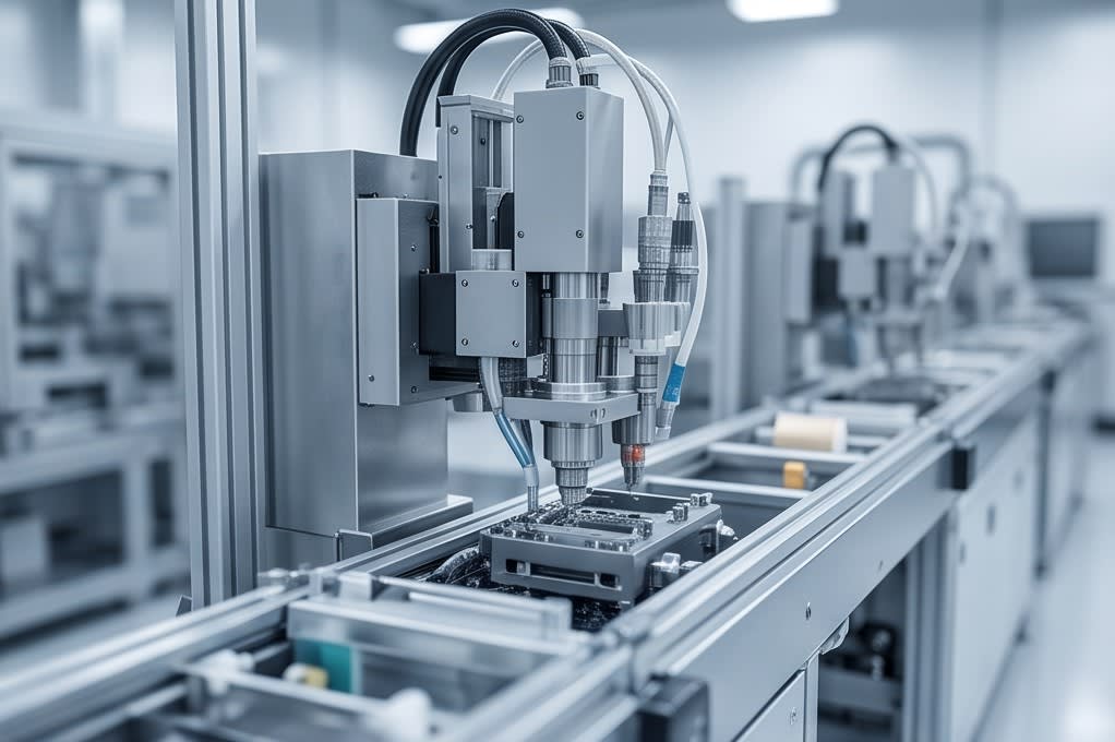
    A wafer moving automatically along a conveyor system while undergoing a precision process.

    As chips become thinner and stacked structures become more complex, actual yield is determined not only by the precision of grinding and cleaning individually, but by how consistently the two processes are connected as one continuous flow. Minimizing thickness deviation in the initial grinding stage and then finishing the process without contamination in the cleaning stage, only when these two conditions are met together can package reliability be secured. Improving each process individually is not enough. It is necessary to consider the entire flow from grinding to cleaning together from the process design stage.


    Huvics is an advanced technology company that develops and manufactures automation equipment and
    production systems across the semiconductor, LED, Mobile, and Cosmetic industries.
    With top talent and continuous technological innovation, we support customer productivity improvement and
    quality competitiveness.

    Huvics Contact Information

    Phone: 031-374-8285
    Email: cdpark@huvics.com

    Contact Huvics

  • From Semiconductor Cleaning to Grinding, Step-by-Step Process Technologies That Protect Yield

    From Semiconductor Cleaning to Grinding, Step-by-Step Process Technologies That Protect Yield

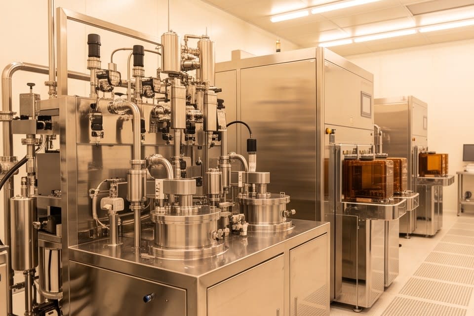
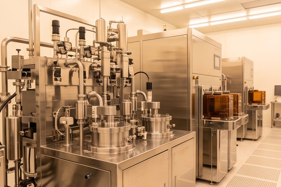
    Semiconductor cleaning equipment implementing a multi-stage cleaning combination

    In semiconductor processes, cleaning was long considered a finishing stage. It was widely viewed as a supporting procedure that removes foreign matter before moving on to the next process. However, as chip integration has increased and package structures have become more complex, we have entered an era where a single cleaning method can determine overall yield. What type of bubbles are used, in what sequence drying takes place, and at what pressure cleaning is performed are now treated as key variables in process design.

    A micro-nano bubble generation scene that removes contamination by distributing fine bubbles in water

    Two Requirements of Cleaning Technology: Removal and Preservation

    The core of cleaning technology lies in removing contaminant particles while fully preserving the product surface. These two requirements conflict with each other. Increasing cleaning power raises the risk of surface damage, while choosing a safer method can leave residual contamination behind.

    The micro jet method instantaneously generates energy reaching thousands of atmospheres and thousands of degrees, and for fine pattern structures below 70 nanometers, this energy itself can become a source of damage. For this reason, in cleaning equipment design, energy control and dispersion methods become key criteria that define the level of technology.

    The micro-nano bubble method distributes bubbles with a diameter of 0.1 micrometers or less in water to separate surface contamination, an approach designed to secure cleaning performance without physical impact. Multi-stage cleaning design combines different principles in this way to respond to the types of contamination generated at each process step.

    For products with complex surface structures and sensitive internal components, such as camera modules, sensors, and VCM motors, the limitations of a single cleaning method are clear. Combining Micro Bubble, Water Jet, and Air Knife step by step, while controlling residual moisture through Oven Dry functionality, is a configuration designed to meet these complex requirements. In processes where cleaning quality is directly linked to the final defect rate, which technology combination to choose is no longer a matter of equipment specifications, but a matter of process strategy.

    A micron-level precision grinding process in which a rotating diamond wheel uniformly processes the substrate surface

    Package Thickness Uniformity and Ultra-Precision Grinding Technology

    Another variable that determines the quality of semiconductor processes as much as cleaning technology is the uniformity of package thickness. In structures where multiple chips are vertically stacked, such as AI semiconductors and high-performance memory, thickness variation in each layer affects both electrical characteristics and mechanical reliability. It is also known that in RF applications, substrate thickness and resistivity affect parasitic capacitance, thereby determining signal integrity.

    The semiconductor industry roadmap requires wafer bonding processes to achieve thickness uniformity within ±5% across the entire wafer surface. If this standard is not met, stacking itself becomes meaningless.

    Huvics PKG Grinder performs micron-level grinding for various package types such as FCBGA, WLCSP, and QFN/DFN by using a high-precision stage and diamond wheel. It is available in Full Auto and Manual Type configurations to secure production line flexibility while being designed to maintain consistent thickness uniformity in high-speed processes. Regardless of which package structure is selected, how tightly thickness variation is managed is the key factor that separates product grade and yield.

    An operator wearing a cleanroom suit manually inspecting a wafer through a microscope

    The Impact of Automation Transition on Yield and Availability

    As the precision of process technology increases, the importance of how equipment is operated to implement it consistently also grows. Processes manually performed by skilled operators rely on individual experience and judgment, which creates structural limitations in repeatability and reproducibility. Even with the same equipment, results vary depending on the operating method, and those differences lead to yield variation in mass-production environments.

    Cases have been reported in which efficiency increased by approximately 17.6% when a systematic yield improvement framework was introduced compared with manual empirical methods. Automation transition is not simply a matter of increasing speed, but of securing process consistency and predictability. According to a McKinsey report, improving equipment reliability can increase tool availability in fabs by more than 15%. Higher availability means fewer unplanned equipment stops and maintenance gaps, which connects directly to the stability of the overall production plan.

    A configuration that combines Full Auto and Manual options is a strategy for flexibly responding to these needs, and many cases have accumulated in manufacturing sites where the level of process automation has been increased step by step.

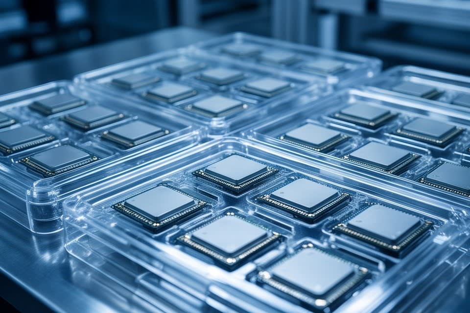
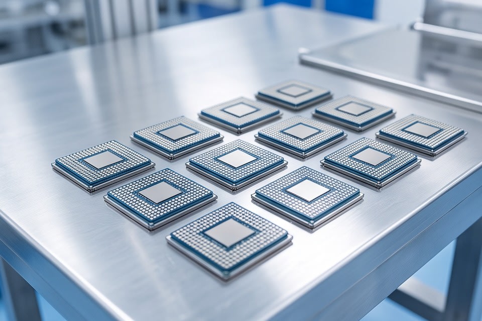
    Semiconductor chips arranged in a tray after securing quality through cleaning and grinding

    In semiconductor processes, cleaning and grinding may appear to be separate technical domains, but they ultimately converge on the same question. How should the surface be handled so that the next process can proceed reliably. Bubble size, pressure control, thickness uniformity, equipment availability, all these variables make up the details of the process, and the sum of those details determines the reliability of the final product. Yield is not reserved at the design stage, but is protected or lost at every step of the process.


    Huvics is an advanced technology company that develops and manufactures automation equipment and
    production systems across the semiconductor, LED, Mobile, and Cosmetic industries.
    With top talent and continuous technological innovation, we support customers in improving productivity and
    securing quality competitiveness.

    Huvics Contact Information

    Phone: 031-374-8285
    Email: cdpark@huvics.com
    Huvics Inquiry

  • Why Process Integration Determines Yield in Semiconductor Cleaning, Grinding, and Lamination

    Why Process Integration Determines Yield in Semiconductor Cleaning, Grinding, and Lamination

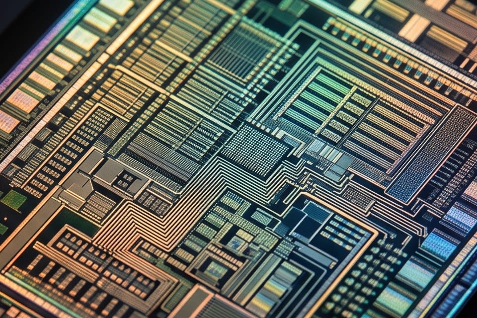
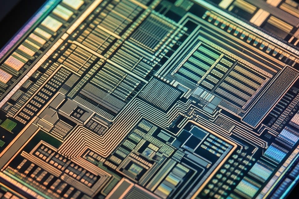
    Finely designed semiconductor circuit patterns

    According to data from Semiconductor Equipment and Materials International (SEMI), a significant share of defects in semiconductor processes is reported to originate from particle contamination. This means that a single particle just a few micrometers in size, invisible to the naked eye, can undermine the yield of an entire chip. As processes become more miniaturized and package structures grow more complex, the precision of each stage, including cleaning, drying, grinding, and lamination, is emerging as a key factor that determines final product quality. By examining which technologies control these variables, we can see the direction in which digital transformation in semiconductor manufacturing is moving.

    Bubbles generated in liquid surrounding a semiconductor substrate

    Structure and Principles of a Multi-Stage Cleaning and Drying System

    Contaminants remaining on semiconductor surfaces are especially difficult to handle because they are not visible. Fine contamination made up of organic matter, metal residues, and particles is difficult to remove through simple physical washing. The approach developed to solve this problem is multi-stage cleaning technology.

    According to a study published in the Korean Journal of Chemical Engineering, a cleaning system using acoustic bubble arrays was shown to remove fine particles of various wettability and sizes with an efficiency of 92.5%. Microbubbles are generated at sizes of 5 nm or less, physically and chemically separating oils and fine particles from the substrate surface, while the following water jet pushes away suspended contaminants. In the air knife stage, remaining moisture and particles on the surface are removed by airflow, and the final oven drying process completely evaporates any moisture left after cleaning.

    Huvics’ 4-stage cleaning and drying system is designed to process this sequence within a single line. For automotive electronics components such as camera modules or autonomous driving sensors, which require both optical cleanliness and electrical reliability, a structure that continuously controls the process through drying is especially important. This is because residual moisture can lead to poor adhesion or corrosion in subsequent processes. The industry is shifting from a method that separated cleaning and drying into individual processes toward an integrated inline system.

    Processing the surface of a semiconductor wafer with a metal wheel and rotating tool

    Grinding and Lamination That Improve Package Process Precision

    As demand for AI semiconductors and high-performance memory increases, package structures are becoming increasingly complex. This is because the mainstream is shifting away from enclosing a single chip in encapsulant and toward structures that vertically stack multiple chips. This change is fundamentally raising the requirements for the grinding process.

    Thickness Uniformity in the Grinding Process

    In stacked packages, even a thickness deviation of only a few micrometers in each layer can directly lead to electrical connection defects or heat dissipation issues. According to published data from the patent office, rough grinding in the package grinding process takes about 2.5 to 5 minutes, while finish grinding takes about 2 to 4 minutes. The key is achieving the target thickness uniformly within this short time. Because required thickness and surface roughness differ by package type, such as FCBGA, WLCSP, and QFN/DFN, equipment must be able to combine diamond wheels with high-precision stages and set conditions differently at the micron level.

    Integrated Structure of the Lamination Process

    The same applies to the lamination process. If equipment is changed at each stage from tape mounting to UV curing, alignment errors accumulate between processes. To reduce this, a one-stop structure that processes everything from the expander to UV curing within a single system is being introduced. How well the processes can be integrated and how precisely the conditions of each stage can be controlled is the key factor that determines next-generation package yield.

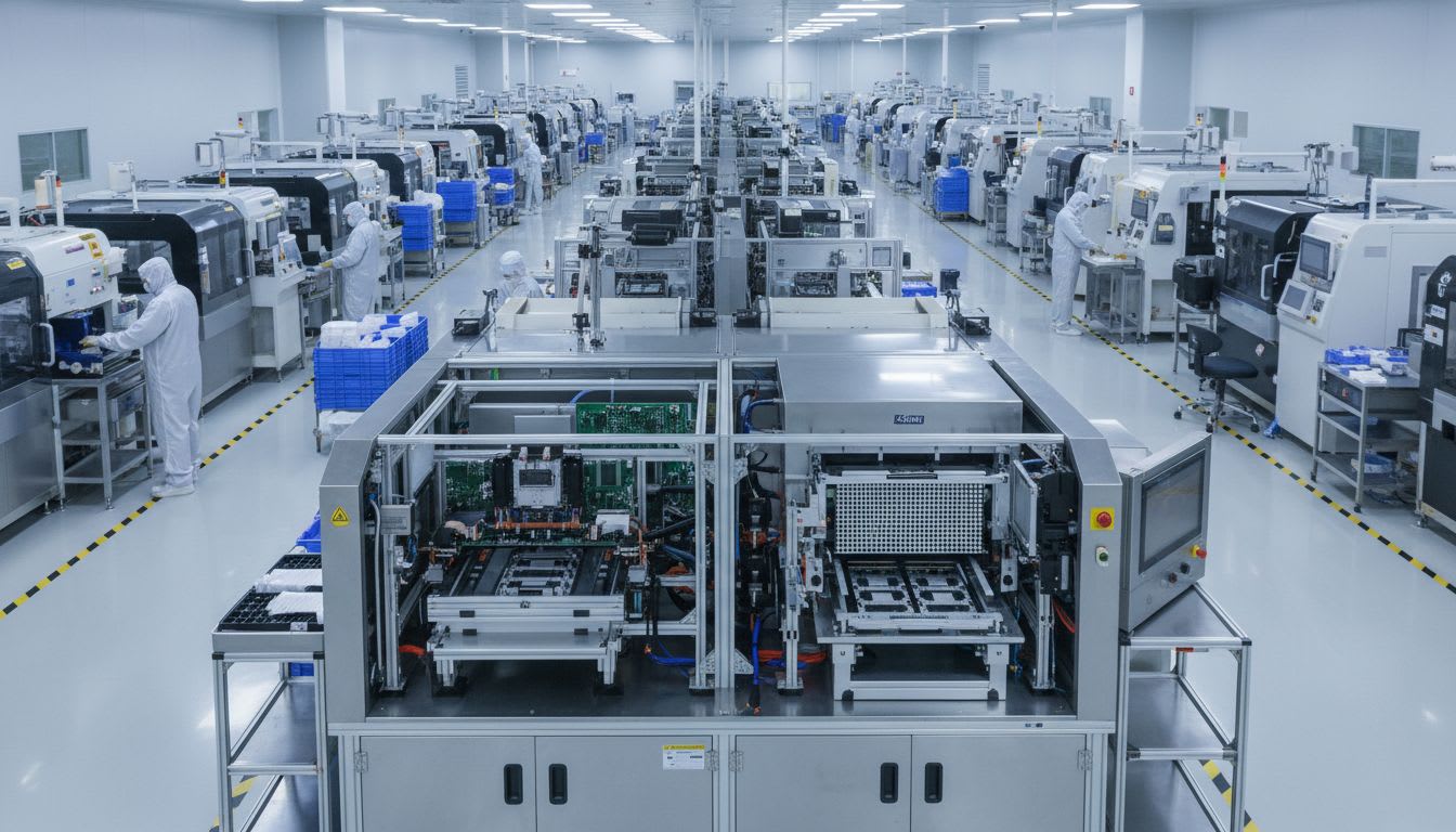
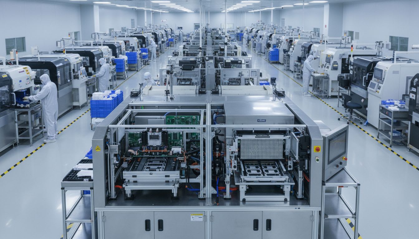
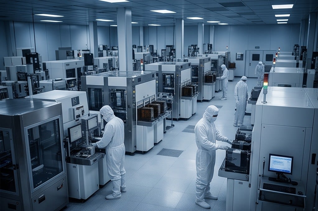
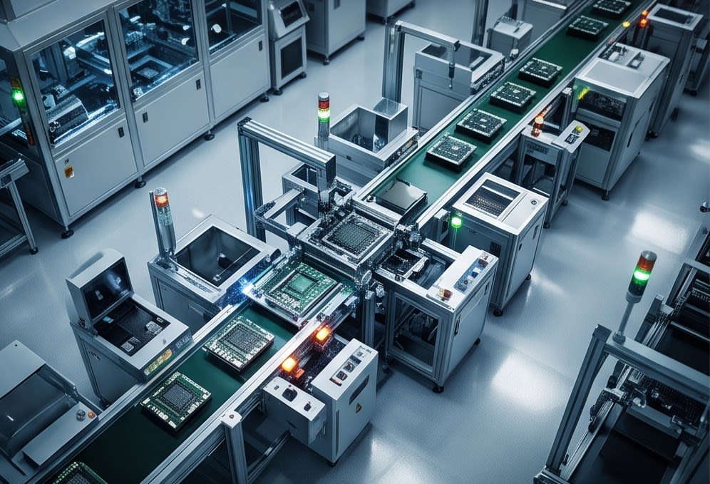
    Overview of a manufacturing site with automated equipment arranged in a row

    Cleaning, grinding, and lamination may appear to be independent processes, but these three stages are connected as one quality chain. If the surface is not completely cleaned, grinding precision becomes unstable, and if thickness after grinding is not uniform, lamination adhesion becomes uneven. Digital transformation in semiconductor manufacturing is not an abstract concept. It begins with precisely controlling each of these connected links through data and automation.


    Huvics is an advanced technology company that develops and manufactures automation equipment and
    production systems across the semiconductor, LED, Mobile, and Cosmetic industries.
    With top talent and continuous technological innovation, we support customers in improving productivity and
    securing quality competitiveness.

    Huvics Contact

    Tel: 031-374-8285
    Email: cdpark@huvics.com

    Huvics Inquiry

  • Why Process Design Determines Yield in Semiconductor Cleaning and Lamination: Field Cases

    Why Process Design Determines Yield in Semiconductor Cleaning and Lamination: Field Cases

    A manufacturing site where various ultra precision electronic components such as camera modules are aligned

    In the past, the cleaning process for semiconductor components was regarded as a supporting task that simply washed away foreign matter. However, as component integration has increased and package structures have become more complex, the cleaning process has emerged as a key variable that determines yield and reliability. Now that components such as MLCC, FPCB, and camera modules, which require micron-level tolerances, have become mainstream, the scope and precision that cleaning technology must handle have fundamentally changed.

    Equipment showing an advanced precision cleaning process as micro bubbles are generated

    The new standards for cleaning technology shaped by miniaturization and high integration

    The miniaturization and high integration of semiconductor components have changed the very nature of contamination that the cleaning process must address. In an environment where a single particle of several tens of micrometers or less can lead to pattern shorts or bonding defects, simple spraying of cleaning solution is not enough to control surface contamination sufficiently.

    According to a study published in the Korean Journal of Chemical Engineering, a cleaning method using a micro bubble array achieved a cleaning efficiency of up to 92.5% and produced a jet velocity up to 5 times higher than that of a single cylinder structure. As the precision of the physical cleaning mechanism increases, particle removal efficiency rises as well.

    In manufacturing sites for ultra precision components such as camera modules, sensors, and VCM motors, the surface condition after cleaning directly affects the final assembly yield. As process environments become more demanding, the criteria for selecting cleaning technology must go beyond simple specification comparisons. Across the industry, the combination of cleaning methods is increasingly determined by the type of contamination being handled as well as the shape and material of the component.

    Automated equipment with ultrasonic dispersion and vision inspection systems operating a robotic arm

    The combination of ultrasonic dispersion and vision inspection

    One of the keys to improving the precision of the cleaning process lies in how uniformly particles in the liquid phase can be controlled. If particles agglomerate or become unevenly distributed in the cleaning solution, the cleaning energy applied to the surface becomes inconsistent, leaving contamination in specific areas.

    This is also why frequency selection is important in ultrasonic cleaning. For substrates with integrated precision circuit patterns such as FPCB, frequencies in the 35~40kHz range are suitable because they provide gentle cleaning energy while effectively separating fine contaminant particles.

    Huvics’ independently developed ultrasonic dispersion technology uniformly disperses material particles in the liquid phase at the micron level, stabilizing the physical properties of materials. When combined with vision inspection algorithms, it detects defects in remaining fine patterns after cleaning in real time and prevents defective products from moving on to the next process.

    Just as the uniformity of particle dispersion in the MLCC process leads directly to the stability of electrical characteristics, cleaning technology and inspection technology must operate within a single loop to substantially control quality variation. Whether the two technologies exist independently or are organically connected within the process flow is the key criterion in selecting a cleaning solution.

    Cleaning solution being precisely sprayed onto components inside a multi stage cleaning system

    The multi stage structure of the Cleaner System and criteria for application decisions

    The choice of cleaning method depends on the product shape, contamination type, and production scale. In structures where lenses and sensors are positioned close together, such as camera modules, the penetration path and discharge direction of the cleaning solution must be precisely designed. For components with large surface areas and complex shapes, such as semiconductor trays, a multi stage cleaning method is advantageous.

    The Huvics Cleaner System is composed of a multi stage cleaning structure that combines Micro Bubble, Water Jet, and Air Knife, and it completes the process flow through drying with an Oven Dry function at the end of the line. According to industry cases, processes that introduced UHP water jet cleaning reported a 40% reduction in cleaning preparation time. With both Full Auto and Manual options, the line can be configured according to production scale and automation level.

    Rather than looking only at cleaning efficiency, it is worth considering an approach that also designs the surface condition after drying and the connection with subsequent processes.

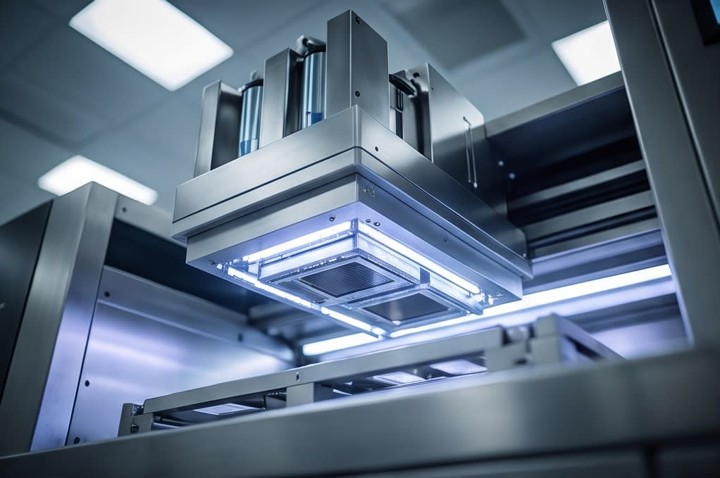
    A UV curing process in which a flat material is exposed under an ultraviolet light source

    The impact of integrated lamination processes on packaging quality

    The lamination process determines the quality of semiconductor packaging from a direction different from cleaning. When tape or protective film is precisely attached to a wafer or substrate, bubbles, wrinkles, or uneven adhesion can affect the entire subsequent process.

    In particular, UV curing is a step that must secure both adhesive strength and process stability, and curing speed and energy uniformity determine the production rhythm of the entire line. Analyses suggest that semi automatic laminators can improve productivity by up to 50% compared with manual feeding, but as the level of automation increases, process linkage design between equipment becomes more important.

    The Laminator System is designed to integrate key processes from Expander to Tape Mounting and UV Curing within a single system, reducing errors that occur during transfer between processes. Lamp and LED type UV Curing can be selectively applied, allowing curing conditions to be optimized according to component characteristics and adhesive materials.

    Integrating processes does not simply mean reducing the number of equipment units. It means reducing variables between each step and improving the reproducibility of quality, and this is where the significance of integrated lamination design becomes clear.

    A flawless circular surface symbolizing perfect surface control in semiconductor packaging and cleaning processes

    Cleaning and lamination may seem like separate processes, but ultimately they pursue the same goal. They control the surface condition and prepare the next process to begin under optimal conditions. As semiconductor components become smaller and more complex, the precision of this preparation carries greater weight in determining overall yield. What today’s manufacturing sites require is not merely choosing a specific technology, but designing the entire process as one continuous flow.


    Huvics is an advanced technology company that develops and manufactures automation equipment and
    production systems across the semiconductor, LED, Mobile, and Cosmetic industries.
    With top talent and continuous technological innovation, Huvics supports customers in improving productivity and
    securing quality competitiveness.

    Huvics Contact

    Phone: 031-374-8285
    Email: cdpark@huvics.com

    Huvics Inquiry

  • Are You Properly Managing the 2 Key Processes That Determine Semiconductor Packaging Yield

    Are You Properly Managing the 2 Key Processes That Determine Semiconductor Packaging Yield

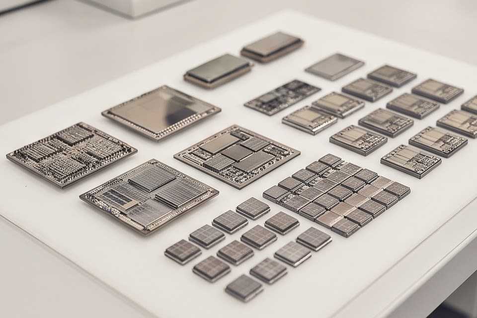
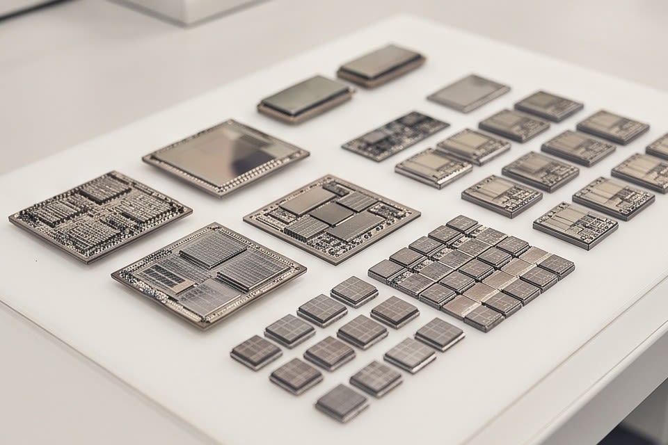
    Semiconductor package samples arranged in various sizes and shapes

    In the semiconductor industry, ‘packaging’ was long regarded as a finishing step placed behind design and process work. However, as demand for AI accelerators and high-performance memory has surged, the situation has changed rapidly. Product competitiveness now depends not only on the performance of a single chip, but on how precisely multiple chips are stacked and connected. Packaging technology now stands at the center of a technology race as intense as semiconductor design itself.

    A diamond wheel uniformly grinding the surface of a semiconductor wafer

    Why Ultra-Precision Grinding Determines Yield

    High-bandwidth memory used in AI accelerators must process more than 1TB of data per second through a vertically stacked structure. To meet this requirement, each stacked chip must have uniform thickness, and surface flatness must also be controlled at the micron level. According to Mordor Intelligence, 3D stacked memory accounts for 34.28% of revenue share in the advanced semiconductor packaging market as of 2025, establishing itself as the leading technology.

    As package formats diversify, such as FCBGA, WLCSP, and QFN, thickness precision standards also vary by type. For example, WLCSP requires a fine pitch between 0.3mm and 0.5mm. Ultimately, grinding precision in the packaging process is a key variable that determines yield. Even a slight increase in thickness variation can undermine the electrical reliability of the entire stacked structure, directly leading to performance degradation in the final product.

    Huvics PKG Grinder responds to these standards with micron-level grinding using a diamond wheel. It is available in both Full Auto and Manual configurations, allowing flexible application according to the production line structure of each customer, while maintaining stable quality even in high-speed processes to achieve high yield. Machining precision is product reliability is the principle that most clearly explains the role this equipment plays in semiconductor packaging processes.

    A cleaning process that sprays liquid onto a semiconductor surface to remove contaminant particles

    Why the Cleaning Process Is the Starting Point of Quality

    If grinding determines the form of packaging, cleaning is the process that ensures this form can perform its intended function. A single fine particle remaining on the semiconductor surface can contaminate the entire subsequent process or lead to defects in the final product. Especially in components that require optical precision, such as camera modules or autonomous driving sensors, invisible contamination can quietly erode product reliability. This is why the cleaning process must be treated not as simple washing, but as the starting point of quality stability.

    Huvics Cleaner System removes contaminant particles from product surfaces by sequentially combining Micro Bubble, Water Jet, and Air Knife, and consistently handles the drying process through its Oven Dry function. Cleaning conditions can be configured differently according to product types such as camera modules, sensors, VCM motors, and trays, enabling a single system to address diverse process requirements.

    In practice, many cases have shown that defects occurring in semiconductor tape bonding processes and yield loss in camera modules can be resolved by improving the cleaning process. Reducing particles reduces defects, and reducing defects increases yield. Engineers who have worked with cleaning processes know well how difficult it is to implement this simple connection in the field. The significance of precision cleaning is confirmed by the fact that it is not the end of the process, but the foundation of quality.

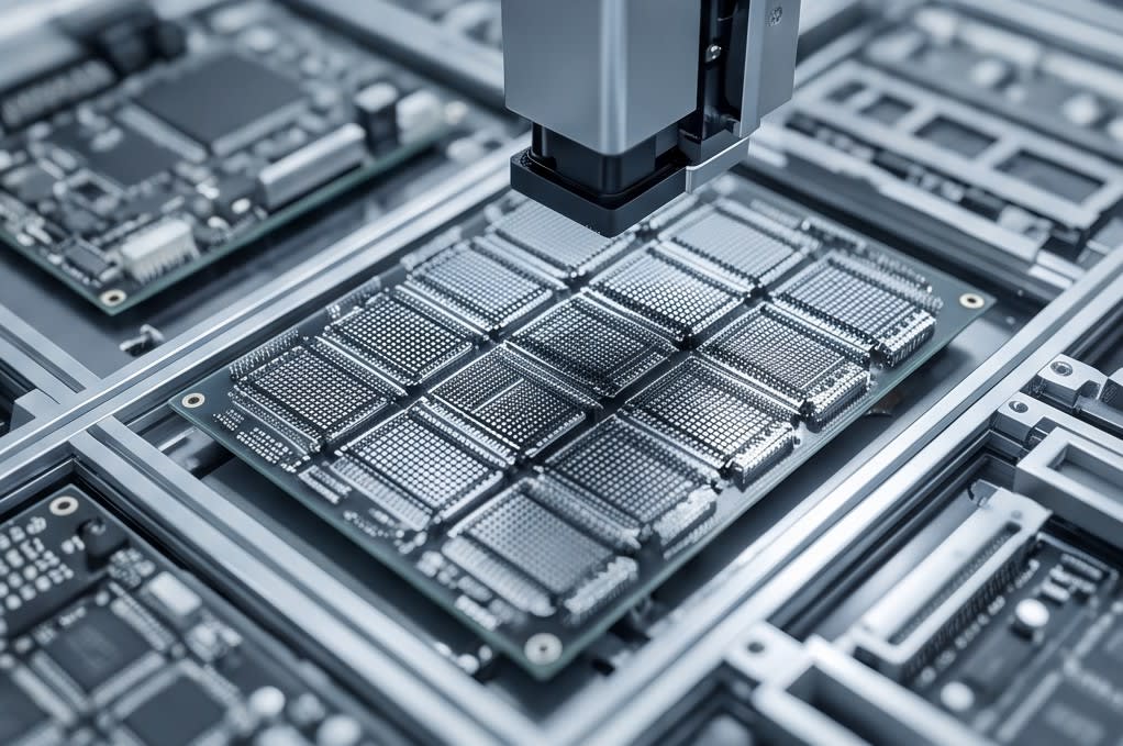
    Precisely processed semiconductor packages arranged in a row

    The competition in semiconductor packaging technology is now shifting toward process precision as much as chip design. Grinding and cleaning are the two pillars that support yield and reliability in this competition. If either one becomes unstable, even the most sophisticated package design will struggle to deliver its intended performance in the field. In an era when technological precision becomes product competitiveness, how firmly each and every process is built will ultimately determine a company’s position in the future semiconductor market.


    Huvics is an advanced technology company that develops and manufactures automation equipment and
    production systems across the semiconductor, LED, Mobile, and Cosmetic industries.
    With top talent and continuous technological innovation, we support customers in improving productivity and
    securing quality competitiveness.

    Huvics Contact

    Tel: 031-374-8285
    Email: cdpark@huvics.com

    Contact Huvics

  • How can ultra precision machining, cleaning, and process integration increase both yield and quality reliability?

    How can ultra precision machining, cleaning, and process integration increase both yield and quality reliability?

    Until now, many manufacturing sites have focused on increasing machining precision while placing cleaning and process integration at a lower priority. Even if equipment performance is improved, if the connection between processes is broken or microscopic contamination remains in the cleaning stage, the precision achieved with great effort cannot translate into yield. Now is the time for an approach that designs machining, cleaning, and process integration as one continuous flow.

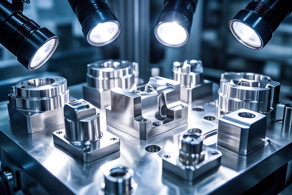
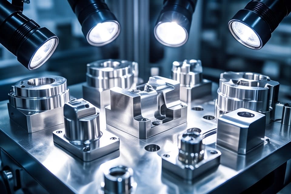
    Precisely machined metal components revealed under lighting.

    Why ultra precision machining has become a basic requirement in modern manufacturing

    As semiconductor packaging technology advances, the allowable range of machining error continues to narrow. In the past, tolerances of several tens of microns were sufficient, but in structures that vertically stack dozens of chips, such as AI semiconductors and high performance memory, the uniformity of package thickness determines the reliability of the entire product.

    Ultra precision machining operates at tolerance levels of ±0.001mm, or 1 micron, or less, and the latest research is expanding into areas that require dimensional tolerances below 10 nanometers and atomic level surface smoothness. As package types become more diverse, including FCBGA, WLCSP, and QFN·DFN, the grinding precision required for each structure also varies.

    When errors invisible to the eye accumulate within a stacked structure, they affect both the electrical characteristics and mechanical durability of the final product. This is not simply a matter of equipment performance, but an issue across the entire process design. Grinding methods that combine diamond wheels with high precision stages have evolved to maintain stable quality even during high speed processes in order to meet these requirements. The trend is already clear: securing machining precision is no longer an option in modern manufacturing, but a basic requirement.

    The surface of a semiconductor component where cleaning fluid is precisely sprayed through a spray nozzle.

    How the cleaning process determines yield and quality reliability

    No matter how high machining precision becomes, yield collapses if microscopic contamination remains in the cleaning stage. Particle Removal Efficiency, or PRE, a key metric used in semiconductor cleaning processes, is a standard that numerically indicates how much contaminant particles have been removed from the surface of wafers or components. According to TSI analysis, particles left behind due to insufficient cleaning can cause critical defects in later processes, and continuous PRE monitoring is essential for maintaining yield and minimizing defects.

    Research findings show that particle removal efficiency typically reaches more than 99%, but decreases to around 94% for ultrafine particles at the 0.064 micron level. As particle size becomes smaller, removal difficulty increases, and the design of the cleaning method must become more precise.

    A multi stage cleaning method that combines micro bubbles, water jet, and air knife is a technical approach for responding to this ultrafine contamination, delivering effectiveness across a wider range of particle sizes than a single method. The drying process after cleaning also plays an important role in preventing contamination from reattaching, and if this stage is incomplete, the cleaning effect is reduced. For components where surface cleanliness is directly linked to performance, such as camera modules, autonomous driving sensors, and VCM motors, the design level of the cleaning process becomes the key factor that determines final quality.

    An automated line where process stages such as grinding, lamination, and cleaning are organically connected.

    Process design that connects grinding, lamination, and cleaning into one flow

    Anyone responsible for a manufacturing site knows well that process defects rarely originate from a single cause. Defects in the semiconductor tape bonding process may be problems with the bonding itself, but they are also often caused by surface conditions before attachment or mismatched UV curing conditions. Tray cleaning challenges also cannot be solved simply by replacing cleaning equipment unless contamination types and material characteristics are considered together. In this way, process defects are often not problems of one specific stage, but occur across the entire connected flow.

    Based on this field context, Huvics adopts a method of designing grinding, lamination, cleaning, and drying processes as one flow. A one stop lamination process that continues from the Expander to UV curing reduces gaps between process stages to shorten tact time, the unit time required to produce one product, and enables an integrated response to issues involving complex causes, such as improving the defect rate of camera modules. The ability to flexibly select Full Auto and Manual configurations also makes it possible to adjust solutions to the practical conditions of the production line. These cases show where the starting point lies for reducing defects already anticipated in process design.

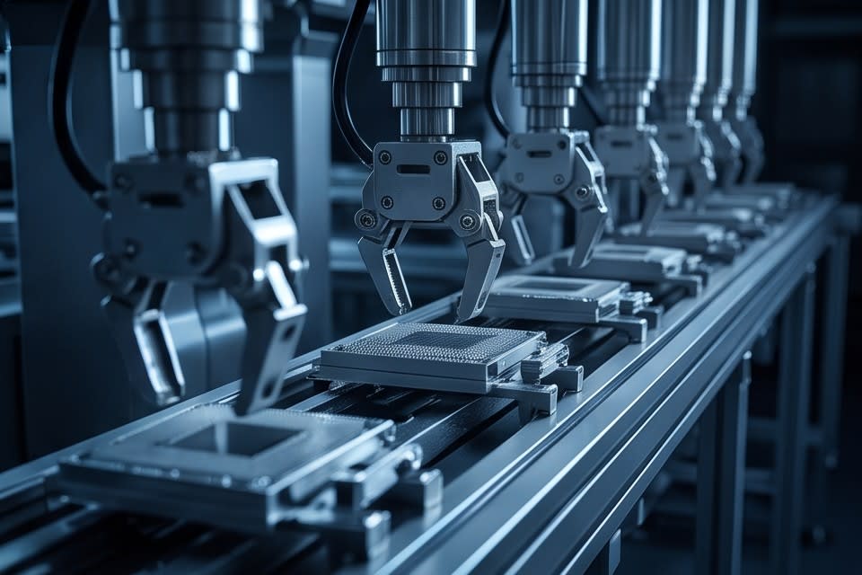
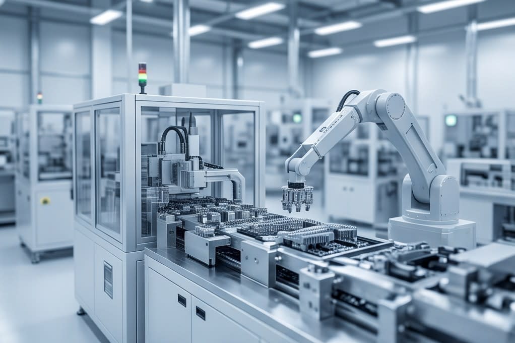
    Multiple robot grippers moving and processing precision components in a row.

    Machining precision, cleaning efficiency, and process integration may seem like separate tasks, but in actual manufacturing sites they are one connected issue. Securing micron level grinding tolerances, designing a cleaning process that removes even ultrafine particles, and connecting each stage without interruption is the way to increase both yield and quality reliability. For manufacturing to maintain a technological edge in global competition, it needs a perspective that views these three elements as one continuous flow.


    Huvics is an advanced technology company that develops and manufactures automation equipment and
    production systems across the semiconductor, LED, Mobile, and Cosmetic industries.
    With top talent and continuous technological innovation, we support customers in improving productivity and
    securing quality competitiveness.

    Huvics Contact Information

    Phone: 031-374-8285
    Email: cdpark@huvics.com
    Contact Huvics

  • Huvics Equipment Maintenance and Preventive Maintenance Guide for Improving Semiconductor Process Efficiency

    Huvics Equipment Maintenance and Preventive Maintenance Guide for Improving Semiconductor Process Efficiency

    Huvics

    Bottlenecks that occur within complex semiconductor processes are one of the biggest factors that reduce productivity. Even after adopting innovative equipment such as the Huvics one-stop laminator system, many sites face challenges because they are unable to fully utilize the potential of the equipment.

    Success in semiconductor manufacturing depends on how efficiently advanced technology is operated and maintained. Since even a small inspection routine can determine equipment lifespan and affect the stability of the entire process, let us look at management solutions for maximizing process efficiency.

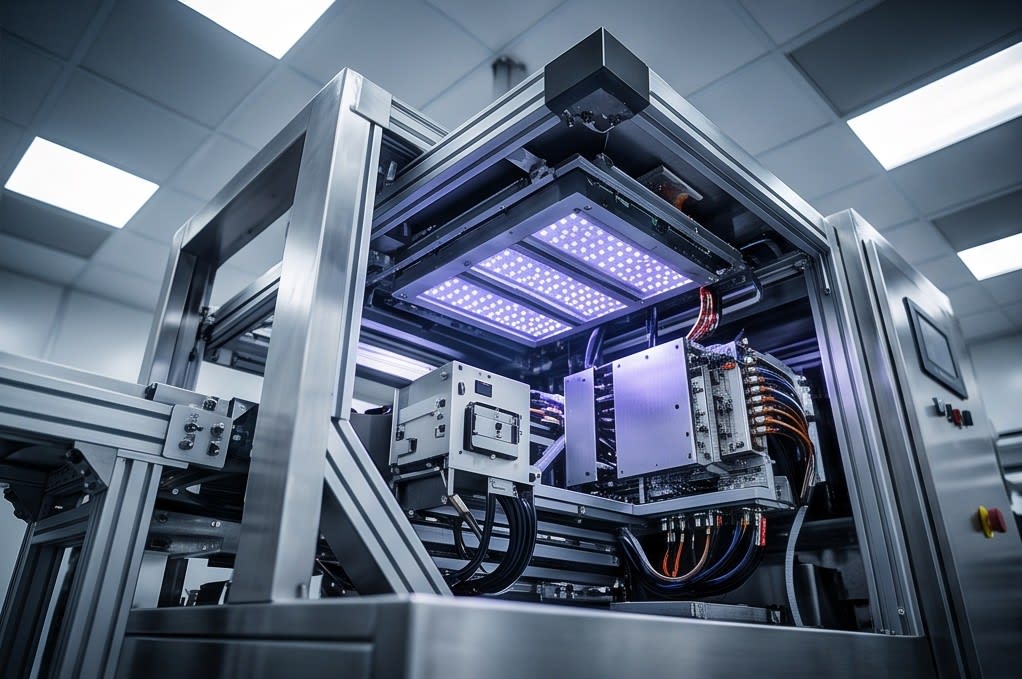
    Core technology of a precision UV curing module

    Huvics Solutions for Semiconductor Process Efficiency

    Resolving Bottlenecks and Integrating Processes

    The most common challenge engineers face in semiconductor manufacturing is bottlenecks that arise between complex process stages. Time delays and transfers that occur while individual equipment performs its functions often become major causes of reduced overall production efficiency.

    To fundamentally solve these issues, Huvics proposes an innovative one-stop laminator system that integrates tape mounting and UV curing into a single process. By unifying previously fragmented processes, this system dramatically reduces product transfer time and maximizes flexibility across the entire production line.

    Technical Advantages and the Importance of Maintenance

    In particular, by precisely controlling adhesive strength through LED-based precision UV curing technology, even microscopic defects that may occur during demanding assembly processes can be prevented at the source. Beyond simply supplying equipment, Huvics aims to become a process optimization partner that helps customers secure the highest yield and stability in any complex process environment.

    However, to fully benefit from these technical advantages, it is essential to clearly understand the core principles of the equipment and perform systematic maintenance by regularly managing the condition of each connection point.

    Internal mechanism of the Huvics system

    Key Management Rules for Extending Equipment Lifespan

    Systematic Management of UV Curing Modules

    To maximize equipment potential and extend its lifespan, the management of LED-based precision UV curing modules plays a decisive role. The key rules for equipment management are as follows.

    • Monitor UV lamp output status in real time to maintain consistent curing quality
    • Establish a regular cleaning routine to prevent the inflow of fine contaminants during production
    • Set parameter values optimized for process objectives to prevent equipment overload

    These small habits become the foundation for strengthening equipment durability and ultimately maximize semiconductor manufacturing quality while improving the stability of the entire process. The maintenance guide provided by Huvics is designed to help customers experience sustainable and high productivity directly in the field.

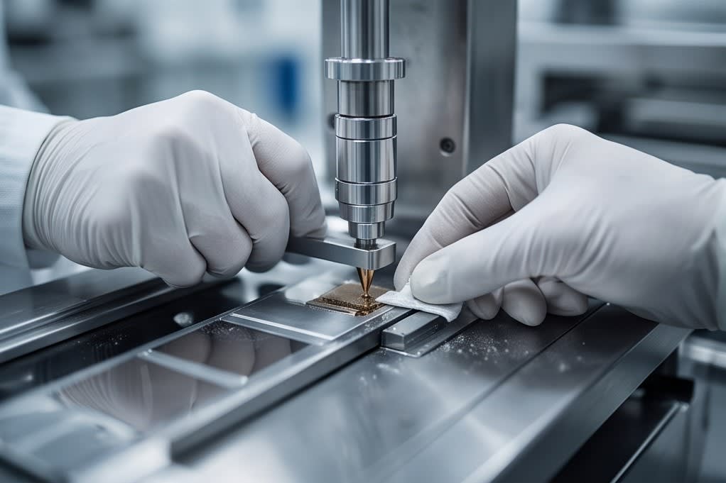
    Precision maintenance work by an engineer

    Strategic Preventive Maintenance for Stable Equipment Operation

    Implementation and Expected Benefits of Preventive Maintenance

    Systematic maintenance goes beyond simply repairing parts. It is a strategic core of Huvics that enables transparent prediction of the flow of the entire process. The recommended practices for reliably utilizing the advanced functions of the Huvics system in the field are as follows.

    1. Strictly follow consumable replacement cycles linked to operating time
    2. Establish regular precision calibration procedures as an internal standard manual
    3. Prevent unexpected downtime through preventive maintenance habits

    Once these preventive maintenance habits are established, unexpected downtime can be prevented in advance. From a long-term perspective, this is the most reliable way to effectively reduce production costs while maintaining consistently high process quality.

    Huvics provides dedicated technical support so customers can eliminate uncertainty from equipment operation and benefit from an optimized manufacturing environment. When thorough preventive maintenance serves as the foundation, equipment delivers its highest performance, which directly leads to business results through sustainable productivity improvement for customers.

    Conclusion for Sustainable Productivity

    The effort to resolve bottlenecks in semiconductor manufacturing ultimately comes down to our attitude toward equipment and careful management routines. Even an innovative tool such as a precision one-stop laminator system can achieve yields and stability beyond expectations only when supported by systematic inspection and maintenance by operators.

    Huvics will stand with customers as a reliable partner so they can remove process uncertainty and maintain the highest productivity. Start a thoughtful preventive maintenance habit today by paying attention to even the smallest movement of your equipment. Those small routines will come together to bring the strongest innovation to your production line.


    Huvics is an advanced technology company that develops and manufactures automation equipment and
    production systems across the semiconductor, LED, Mobile, and Cosmetic industries.
    With top talent and continuous technological innovation, we support improvements in customer productivity and
    quality competitiveness.

    Huvics Contact

    Phone: 031-374-8285
    Email: cdpark@huvics.com

    Huvics Inquiry

  • Core Competitiveness in Advanced Semiconductor Packaging – Huvics PKG Grinder Ultra-Precision Grinding Solution

    Core Competitiveness in Advanced Semiconductor Packaging – Huvics PKG Grinder Ultra-Precision Grinding Solution

    Huvics

    The advanced semiconductor packaging market has become a stage for more intense technological competition than ever before. Today, the value of semiconductors is determined not only by how far they can push performance limits, but also by how thinly and precisely they can be packaged. In particular, thickness uniformity and high flatness, which are required in fine processes, have become essential indicators for securing a technological edge.

    The Importance of Ultra-Precision Grinding Processes

    In the production of next-generation artificial intelligence and high-performance memory semiconductors, the perfection of the grinding process that ensures physical reliability has become a decisive factor that determines the fate of the final product. In response to these demands of the times, Huvics is presenting a new industry standard through its ultra-precision grinding solution, PKG Grinder. Going beyond simply manufacturing machines, Huvics is becoming a reliable partner for companies seeking to overcome technological limits by helping them address the subtle differences found in semiconductor manufacturing sites.

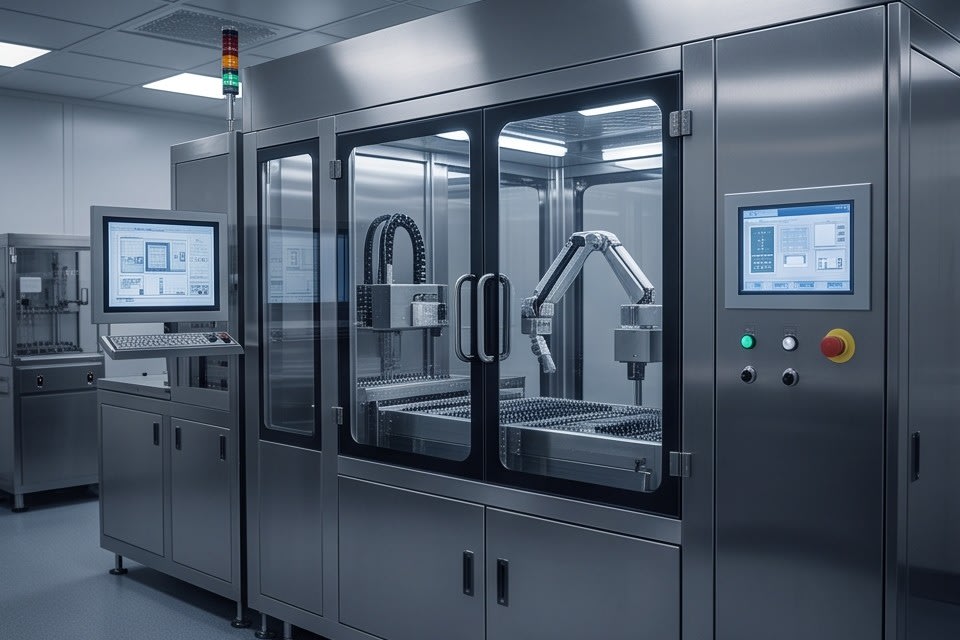
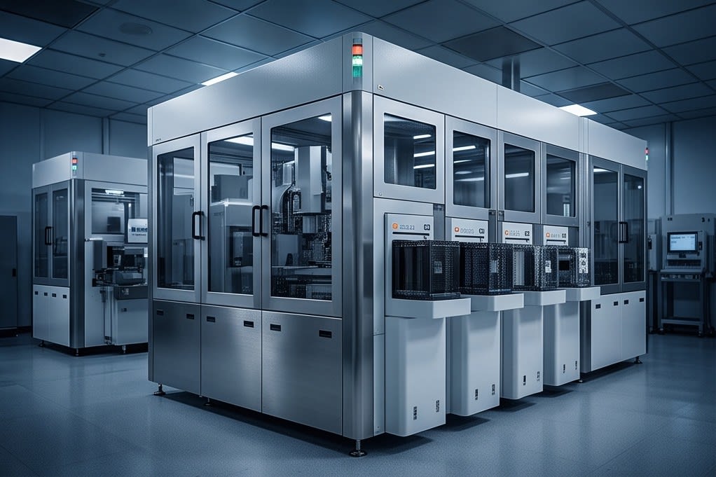
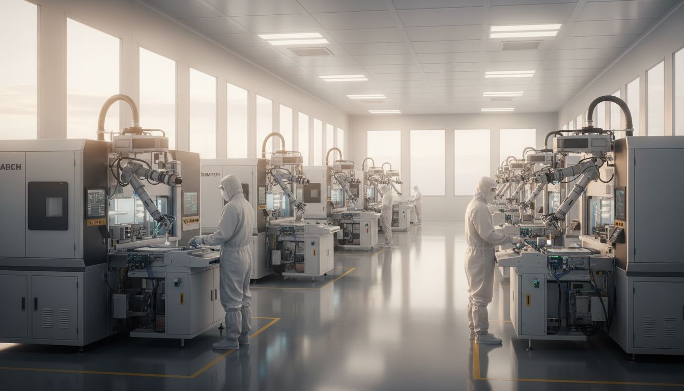
    Precision process in a semiconductor cleanroom

    Technical Strengths of the PKG Grinder

    The greatest strength of the Huvics PKG Grinder lies in the perfect combination of a high-precision stage and advanced diamond wheel technology. This technology, which does not allow even the slightest error during the grinding process, delivers precise grinding at the micron level. When performing advanced package processes such as flip chip ball grid array or wafer-level chip-scale package, maintaining unwavering flatness is essential to maximizing the physical reliability of the product.

    Semiconductors produced with this equipment can maintain consistent performance even under changing external environments or high-speed operating conditions. This improves the durability and efficiency of the products customers bring to market, ultimately leading to a noticeable enhancement in the quality of technology experienced by end users.

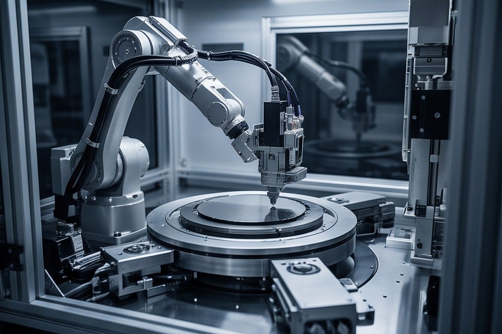
    Operation of an ultra-precision robotic arm

    Customized Production Lineup and Strategy

    Requirements on the production floor vary from company to company. Huvics provides a broad lineup that reflects diverse production scales and characteristics.

    • Support for high-speed automation systems for mass production
    • Detailed control with manual types for special purposes
    • Strategic equipment selection directly connected to production yield
    • Stable quality maintenance in a rapidly changing market environment

    Front view of PKG Grinder equipment

    Technological Competitiveness and Sustainable Growth

    We are now in an era where the precision of equipment directly becomes a company’s competitiveness. The customized solutions from Huvics are not merely auxiliary tools that improve efficiency, but practical weapons that help companies stay one step ahead in global technology competition. By deeply understanding the challenges experienced engineers face in the field and incorporating those insights into equipment design and operation methods, companies can maximize process efficiency.

    The ability to obtain high-quality results that remain stable even in high-speed production environments gives companies the technical confidence they need to advance into broader markets. As a result, this technological support provided by Huvics will drive sustainable corporate growth and become a key force in securing stable market share and product reliability in the advanced semiconductor packaging market.

    In the fierce technological competition to break through the limits of semiconductor packaging, what we must ultimately focus on is how precisely the finest details of the process can be controlled. The Huvics solution, which maximizes the physical reliability of products through ultra-precision grinding technology, goes beyond being a tool for improving efficiency and will become a key driving force for securing unwavering competitiveness in a rapidly changing market environment. Now that small differences in processes are coming together to define the standards of future technology, we invite you to add the most accurate and robust technological answer to your production site with Huvics.


    Huvics is an advanced technology company that develops and manufactures automation equipment and
    production systems across the semiconductor, LED, mobile, and cosmetics industries.
    With top talent and continuous technological innovation, we support customers in improving productivity and
    securing quality competitiveness.

    Contact Huvics

    Phone: 031-374-8285
    Email: cdpark@huvics.com

    Huvics Inquiry

  • Semiconductor Process Automation Solutions – Reduce Labor Costs and Secure Quality Competitiveness with Huvics

    Semiconductor Process Automation Solutions – Reduce Labor Costs and Secure Quality Competitiveness with Huvics

    Huvics

    In semiconductor manufacturing, even a one-second deviation can become a critical variable directly tied to business competitiveness. For manufacturers that must secure profitability while meeting increasingly strict global quality standards, process automation is now an essential strategy for survival.

    Beyond simply replacing equipment, the key is to accurately diagnose bottlenecks on the production floor and achieve both labor cost reduction and quality stabilization. Huvics becomes a reliable partner that elevates your manufacturing environment to the next level by solving technical challenges from semiconductor tape bonding to tray cleaning processes, based on sophisticated data analysis and customized solutions.

    Semiconductor automation process flow

    Automation Strategies That Enhance Semiconductor Manufacturing Competitiveness

    Customized Process Design and Maximum Efficiency

    In the semiconductor manufacturing industry, precision that allows no error even for a single second is essential. In this highly competitive environment, adopting automated equipment has moved beyond simply replacing aging machines or increasing the number of units. It has become a necessary management strategy for securing fundamental manufacturing competitiveness and responding flexibly to market changes.

    Huvics deeply understands the trends of these industrial sites and does not stop at supplying standardized equipment. By precisely diagnosing and analyzing the entire customer process, we propose customized total solutions such as the following.

    • Dramatically reduce unnecessary labor costs
    • Design processes that maximize production efficiency
    • Improve cost structures that hinder profitability
    • Resolve bottlenecks to increase production speed

    Solving Technical Challenges and Success Cases

    Numerous success cases, including overcoming chronic defect issues in semiconductor tape bonding processes and technical limitations in highly difficult tray cleaning processes, prove the differentiated technical capabilities unique to Huvics. Go beyond simple equipment implementation and design your own smart manufacturing environment with Huvics, a true partner that helps customers secure a distinctive advantage on the global stage.

    Precision semiconductor process robot

    Data-Based Quality Stabilization Solutions

    Minimizing Human Error and Ensuring Quality Uniformity

    A significant portion of recurring quality issues in manufacturing ironically begins at the fingertips of people. No matter how skilled an operator may be, performing precise work at the same intensity for long periods leads to fatigue, and during that process, the possibility of subtle errors increases.

    Huvics resolves these deep concerns from the field through technology. By introducing automated processes and minimizing human factors, quality stability is maximized. In particular, converting processes that previously depended only on the experience and intuition of skilled technicians into data-based systems can deliver the following results.

    • Eliminate subtle deviations between operators
    • Produce and maintain identical results every time
    • Secure and maintain product quality uniformity
    • Create an opportunity to dramatically reduce defect rates

    Technology for Achieving Global Quality Standards

    Huvics automation systems go beyond economic tools that simply reduce labor costs. They are powerful technological assets that enable companies to confidently meet the strict quality standards demanded by global markets. As process reliability increases, corporate value rises. Now, strengthen your processes through the smart transition of automation, elevate the standard of quality, and complete your global manufacturing competitiveness.

    Smart automation control system

    After-Sales Management for Sustainable Growth

    Close Technical Support After Equipment Introduction

    It is no exaggeration to say that the true beginning of successful automation is not the moment equipment is installed on site, but the period after the system begins operating. Many companies devote major effort to the equipment introduction process, yet often face unexpected difficulties during operation and maintenance afterward.

    Huvics completes the value of partnership by continuing ongoing management and close technical support even after equipment supply. We do not simply install hardware and end the process. Instead, we carefully ensure that the system settles perfectly into the field and delivers peak performance. The close support solution unique to Huvics includes the following.

    • Stable operation through after-sales maintenance
    • Process improvement through production data analysis
    • Prevention of unexpected production shutdown risks
    • Support based on accumulated technical know-how

    A Reliable Foundation for Smart Factory Implementation

    The extensive technical know-how accumulated in real field environments and a solid support system become a reliable foundation that allows companies to maintain competitive advantage without wavering, even in a rapidly changing industrial environment. When automated equipment introduction is combined with systematic after-sales management, your company can finally implement a true smart factory and establish a firm foundation for sustainable growth.

    Automation equipment and production line

    In semiconductor manufacturing, the challenge of securing every second of efficiency must now be solved through smart process design based on data, beyond simple equipment replacement. The trend of automation that removes unnecessary costs and improves process reliability is an essential choice for your company to secure a distinctive advantage in the global market.

    Huvics will continue to be a reliable partner, helping your processes deliver optimal performance without interruption through precise technology and close after-sales management. Now, strengthen your unique competitiveness through the innovative transition of automation.


    Huvics is an advanced technology company that develops and manufactures automation equipment and
    production systems across the semiconductor, LED, Mobile, and Cosmetic industries.
    With top talent and continuous technological innovation, we support customer productivity improvement and
    the securing of quality competitiveness.

    Huvics Contact Information

    Phone: 031-374-8285
    Email: cdpark@huvics.com

    Contact Huvics

  • Innovation in Semiconductor Manufacturing Processes – Quality Competitiveness Achieved with Huvics Ultrasonic Dispersion and Vision Inspection Solutions

    Innovation in Semiconductor Manufacturing Processes – Quality Competitiveness Achieved with Huvics Ultrasonic Dispersion and Vision Inspection Solutions

    Huvics

    In today’s manufacturing sites for semiconductors and ultra-compact electronic components, even the smallest micro-level deviation has become a decisive factor that determines the quality of the final product. Especially in processes that require high precision, such as multilayer ceramic capacitors and flexible printed circuit boards, uniform material dispersion and defect detection in fine patterns are key challenges that determine the reliability of the entire production process.

    To overcome these technical limitations, Huvics is setting a new standard for manufacturing processes by intelligently integrating its proprietary ultrasonic dispersion technology with advanced vision inspection algorithms. In an era where precision directly defines corporate competitiveness, we take a closer look at Huvics’ unique solutions that are driving innovation in manufacturing quality while working closely with global leading companies.

    Huvics Innovative Quality Control Technology

    Huvics Solutions Driving Innovation in Manufacturing Processes

    Today, as semiconductors and ultra-compact electronic components have become essential to our daily lives, even the slightest deviation in the manufacturing process can become a decisive variable that affects the quality of the final product. In particular, micro-level deviations that are difficult to identify with the naked eye can act as critical factors that undermine the reliability of the entire production line.

    To meet the rigorous standards of this manufacturing environment, Huvics presents innovative solutions that combine ultrasonic dispersion technology with advanced vision inspection algorithms, redefining industry standards.

    Micro-Level Precision Dispersion Technology

    In particular, Huvics’ unique technology for precisely dispersing liquid-based internal materials at the micro level during the manufacturing of multilayer ceramic capacitors (MLCC) and flexible printed circuit boards (FPCB) perfectly ensures uniformity across the entire process. The technical value provided by Huvics is as follows.

    • Fundamentally blocks quality variability that occurs during the production of highly integrated electronic components
    • Significantly reduces process uncertainty experienced by manufacturers
    • Strengthens the structural reliability of components and secures a technological advantage in the global market

    Micro-Level Precision Dispersion Technology

    Defect Control Through Real-Time Vision Inspection

    Furthermore, Huvics’ advanced vision inspection algorithm serves as a powerful engine that maximizes the initial assembly reliability of core components for smart devices. During the rapid assembly of numerous components on manufacturing sites, defects in fine patterns often lead to large-scale failures if they are not detected at an early stage.

    Huvics technology precisely detects these fine pattern defects in real time and thoroughly controls data across the overall process. As a result, it has achieved visible improvements by significantly lowering defect rates on site, which directly leads to cost reduction and productivity improvement for customers.

    Real-Time Fine Pattern Defect Detection

    Global Partnerships and Future Value Creation

    This advanced technology infrastructure is the core driver that enables Huvics to build unrivaled competitiveness in the market while working closely with global leading companies. Huvics’ progress in completing the intelligence of manufacturing processes, rather than remaining a simple equipment supplier, is becoming the foundation of a strong partnership that helps customers grow steadily even in a constantly changing global market environment.

    Technology should go beyond simply performing functions and become a strategic asset that determines the future value of a company. At precisely this point, Huvics provides optimized process solutions that help customers stand tall as global leaders and design the future together.

    Huvics’ continuous research and field-centered approach to enhancing technical completeness will continue to solve complex problems at manufacturing sites one by one and create positive ripple effects across the industry.

    Intelligent Smart Factory Solution

    Ultimately, the subtle differences that determine semiconductor performance begin with perfect process control, and this becomes the key variable that defines global competitiveness. Through an innovative solution that brings together ultrasonic dispersion technology and precision vision inspection, Huvics goes beyond solving process issues and becomes a technological partner that helps manufacturers design a future of higher quality.

    Join Huvics as it continuously pushes beyond technological limits and builds industrial trust, and discover the perfect answer for sustainable growth at your manufacturing site.


    Huvics is an advanced technology company that develops and manufactures automation equipment and
    production systems across the semiconductor, LED, mobile, and cosmetic industries.
    With top-tier talent and continuous technological innovation, we support customers in improving productivity and
    securing quality competitiveness.

    Huvics Contact Information

    Phone: 031-374-8285
    Email: cdpark@huvics.com
    Contact Huvics