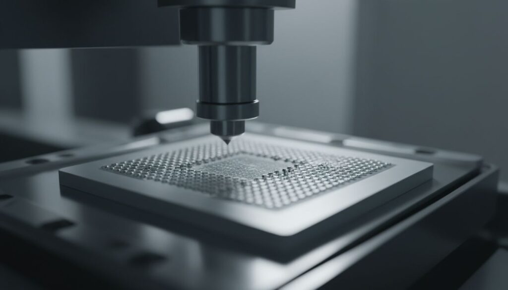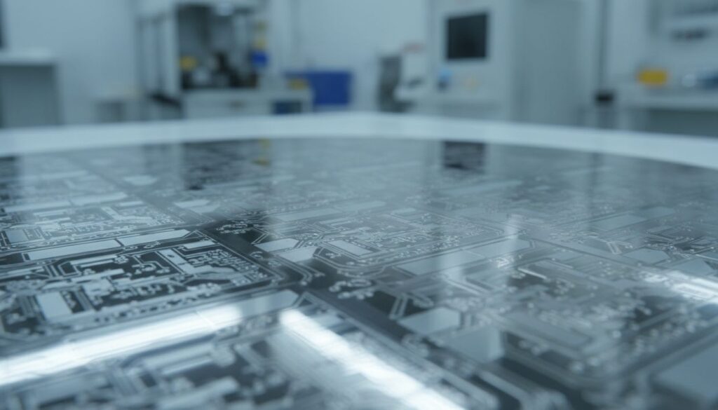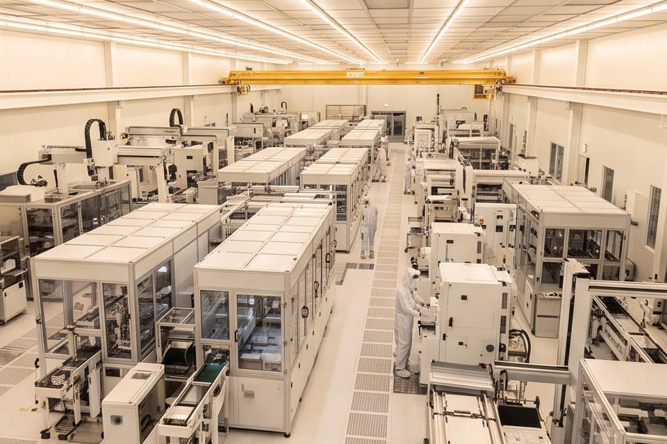
If you discover too late that a thickness deviation of only a few micrometers has occurred during the grinding process, yield loss and rework costs in downstream processes may already have accumulated. Thickness nonuniformity undermines the reliability of the entire chip stacking structure, and once the package is completed, it can lead to defects that are difficult to reverse. If this issue is left unaddressed, it can spread to delivery delays and customer claims, making precise thickness control essential from the very beginning of the process.
Why Thickness Uniformity Matters in Chip Stacking Packaging
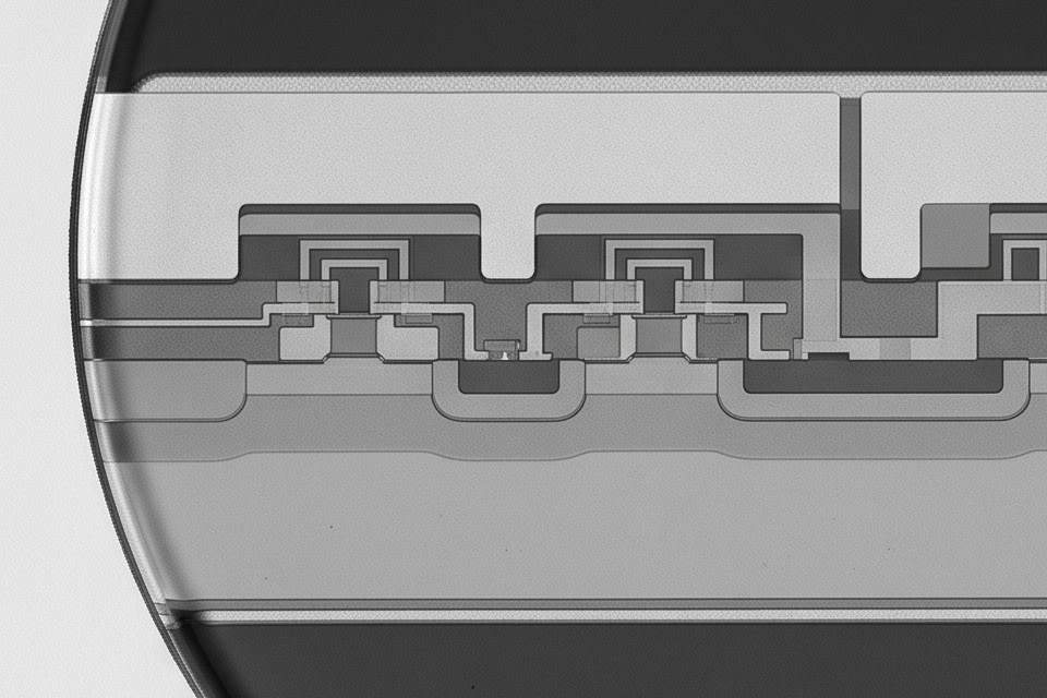
As semiconductor packaging technology evolves into 3D stacked structures, maintaining uniform thickness in each chip has emerged as a key factor that determines overall package performance. In structures where multiple chips are stacked vertically, such as high-bandwidth memory, narrower gaps between chips improve signal transmission quality. However, even a slight thickness deviation increases the risk of bonding defects and warpage.
Across the industry, advanced stacked packaging is moving toward wafer thickness targets in the range of 25 to 50 micrometers. This is less than half the thickness of a human hair, requiring a level of precision that cannot even be verified with the naked eye.
As package formats become more diverse, including FCBGA, WLCSP, and QFN/DFN, the thickness standards and tolerances required for each structure also vary. This is why target thickness and machining strategies must be set differently depending on the package type, even within the same grinding process. Ultimately, securing thickness uniformity in chip stacking packaging is not simply a matter of machining precision. It has become a process design issue that determines product reliability and overall yield.
How the Grinding Process Determines Thickness Uniformity
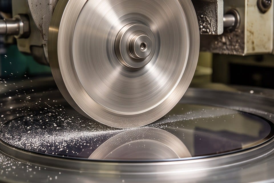
The performance of grinding equipment is evaluated mainly by two factors. One is machining precision, and the other is process stability. A grinding method that combines a high-precision stage with a diamond wheel enables thickness control at the micron level and is advantageous for maintaining uniform flatness across the entire wafer surface.
In WLCSP structures, wafer grinding becomes the core method for reducing the overall package height. In FCBGA structures, the target thickness must be set differently because the package takes advantage of its greater thickness and lower conduction loss. This is why grinding strategies must differ by package type.
To maintain stable quality even in high-speed process environments, the automation level of the equipment becomes an important variable. The Huvics PKG Grinder supports both Full Auto and Manual configurations, allowing flexible response according to the production line type and required yield. The manual method is suitable for low-volume and high-mix production, while the automated method offers strong advantages in minimizing process variation in mass production environments.
The key to yield stability lies in which equipment configuration is selected for the grinding process and how precisely the machining conditions are set for each package type.

Why the Cleaning Process After Grinding Determines Final Quality
The process is not complete even after grinding is finished. If fine particles and surface contaminants generated during grinding are not removed, they become the source of defects in subsequent processes. In manufacturing sites for ultra-precision components such as camera modules and sensors for autonomous driving, where even a single speck of dust is hard to tolerate, companies repeatedly experience yield collapse the moment the cleaning step is omitted. If contaminant particles remain on the bonding surface, they lead to poor electrical contact, and in optical components, they directly cause image quality degradation.
A multistage cleaning method that combines microbubbles, water jets, and air knives step by step removes fine contamination on the product surface in different ways at each stage, securing higher particle removal efficiency than a single cleaning method. After cleaning, a drying process must follow to completely remove residual moisture, and equipment integrated with an oven drying function can handle these two steps within one continuous flow.
Huvics has applied solutions tailored to different contamination conditions and cleaning requirements at each site, including cases involving semiconductor tray cleaning and camera module defect improvement. Since cleaning conditions vary depending on product type and process environment, reviewing both equipment flexibility and site suitability leads to practical quality improvement.

As chips become thinner and stacked structures become more complex, actual yield is determined not only by the precision of grinding and cleaning individually, but by how consistently the two processes are connected as one continuous flow. Minimizing thickness deviation in the initial grinding stage and then finishing the process without contamination in the cleaning stage, only when these two conditions are met together can package reliability be secured. Improving each process individually is not enough. It is necessary to consider the entire flow from grinding to cleaning together from the process design stage.
Huvics is an advanced technology company that develops and manufactures automation equipment and
production systems across the semiconductor, LED, Mobile, and Cosmetic industries.
With top talent and continuous technological innovation, we support customer productivity improvement and
quality competitiveness.
Huvics Contact Information
Phone: 031-374-8285
Email: cdpark@huvics.com