Tag: Packaging

  • AI Semiconductor Packaging Yield: How to Improve It Step by Step from Grinding to Cleaning

    AI Semiconductor Packaging Yield: How to Improve It Step by Step from Grinding to Cleaning

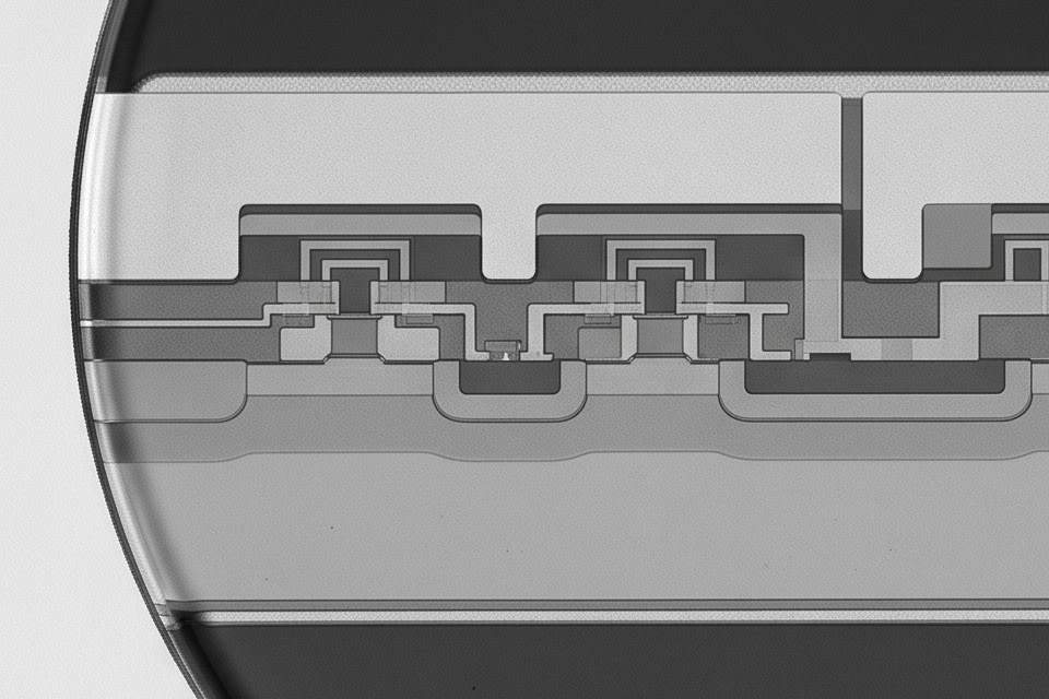
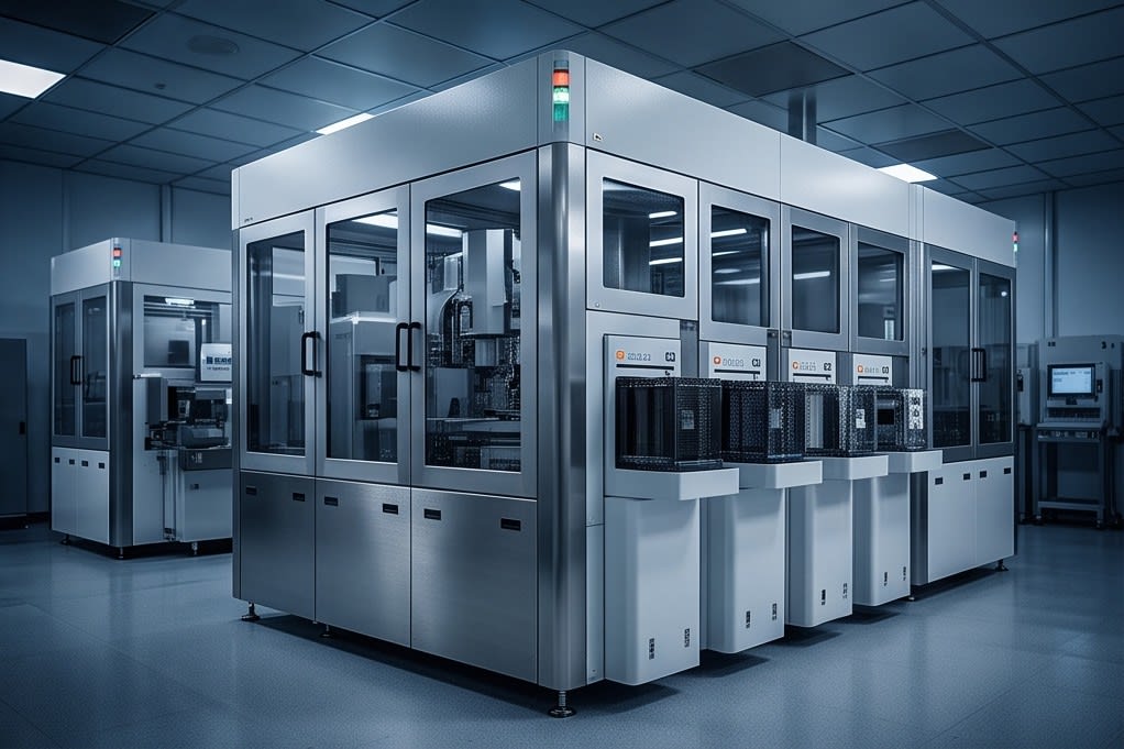
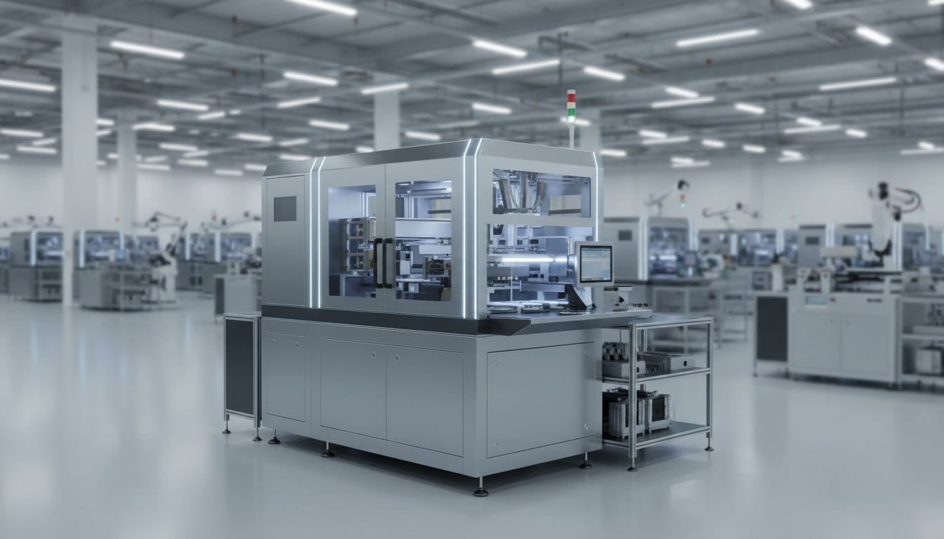
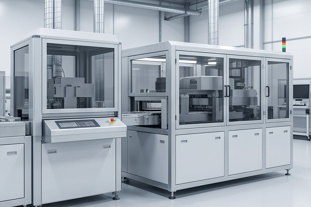
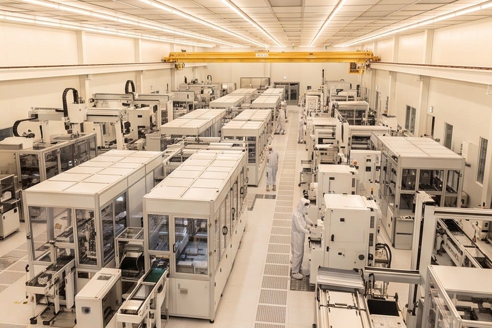
    A semiconductor packaging process site where multiple pieces of equipment are organically connected

    When I first looked closely at a semiconductor packaging site, there was one question customers commonly asked. “The grinding went well, so why do defects keep appearing during bonding?” That question once again confirmed that the root of the problem is not a single piece of equipment, but the entire flow of the process. At that site, I learned firsthand that even a slight deviation in flatness can affect every layer built on top of it.
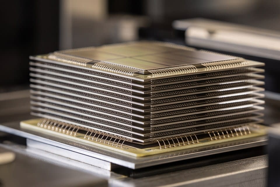
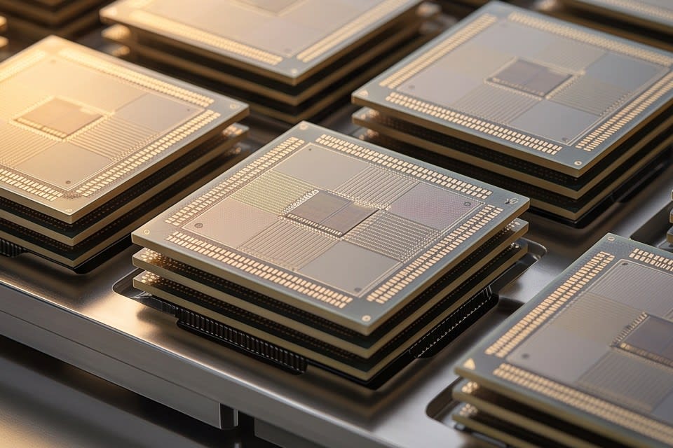
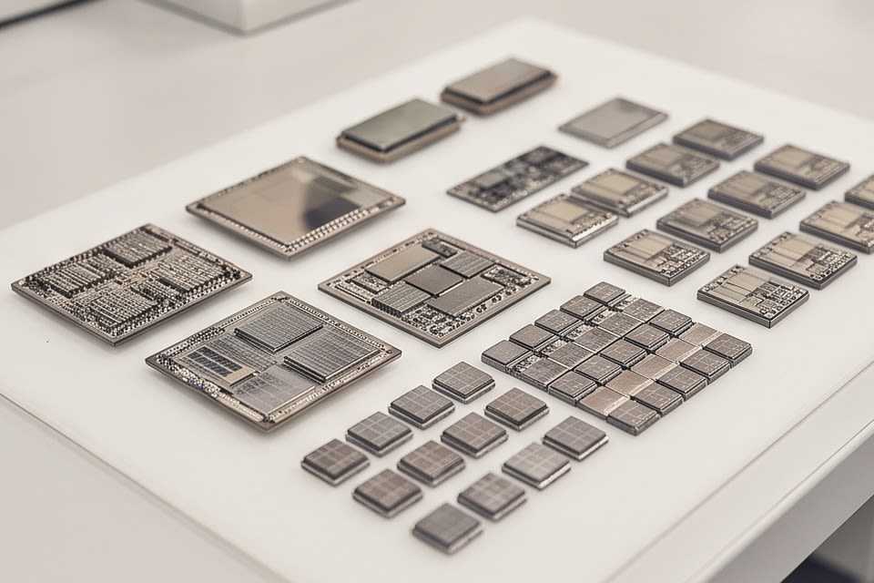
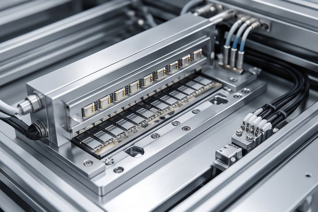
    A semiconductor stacked structure with dozens of dies precisely stacked vertically

    Why flatness is critical in AI semiconductor packaging

    HBM(High Bandwidth Memory), now a core component of artificial intelligence semiconductors, is built by vertically stacking dozens of thin dies. In a 12 layer stack, each die is about 50 micrometers thick, but when the stack increases to 16 layers, the die must be thinned to about 30 micrometers. As the die becomes thinner, the rigidity of the wafer itself decreases, and the risk of warpage and cracking during the process increases as well.

    Variation in surface flatness is not simply a dimensional issue. According to a technical report from Applied Materials, even minute surface variations directly affect bonding quality and yield. As the number of stacked layers increases, the requirements for thickness uniformity in each layer become stricter, and tolerances become narrower. As package types such as FCBGA, WLCSP, and QFN become more diverse, these requirements become even more complex. Ultimately, flatness control in the packaging process is not optional. It is a variable that determines yield itself.
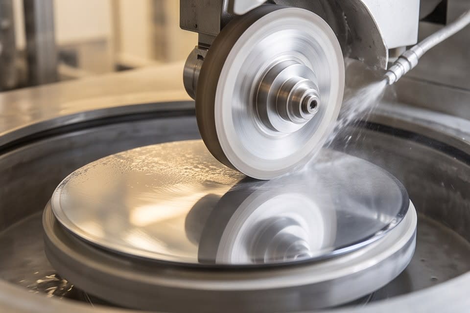
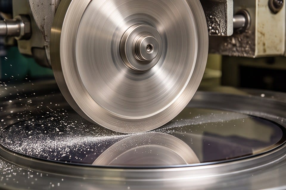
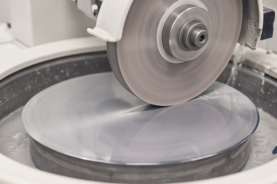
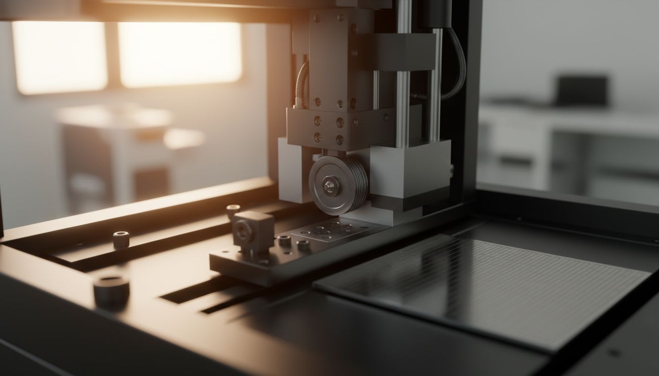
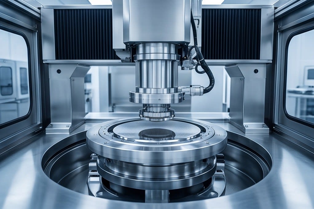
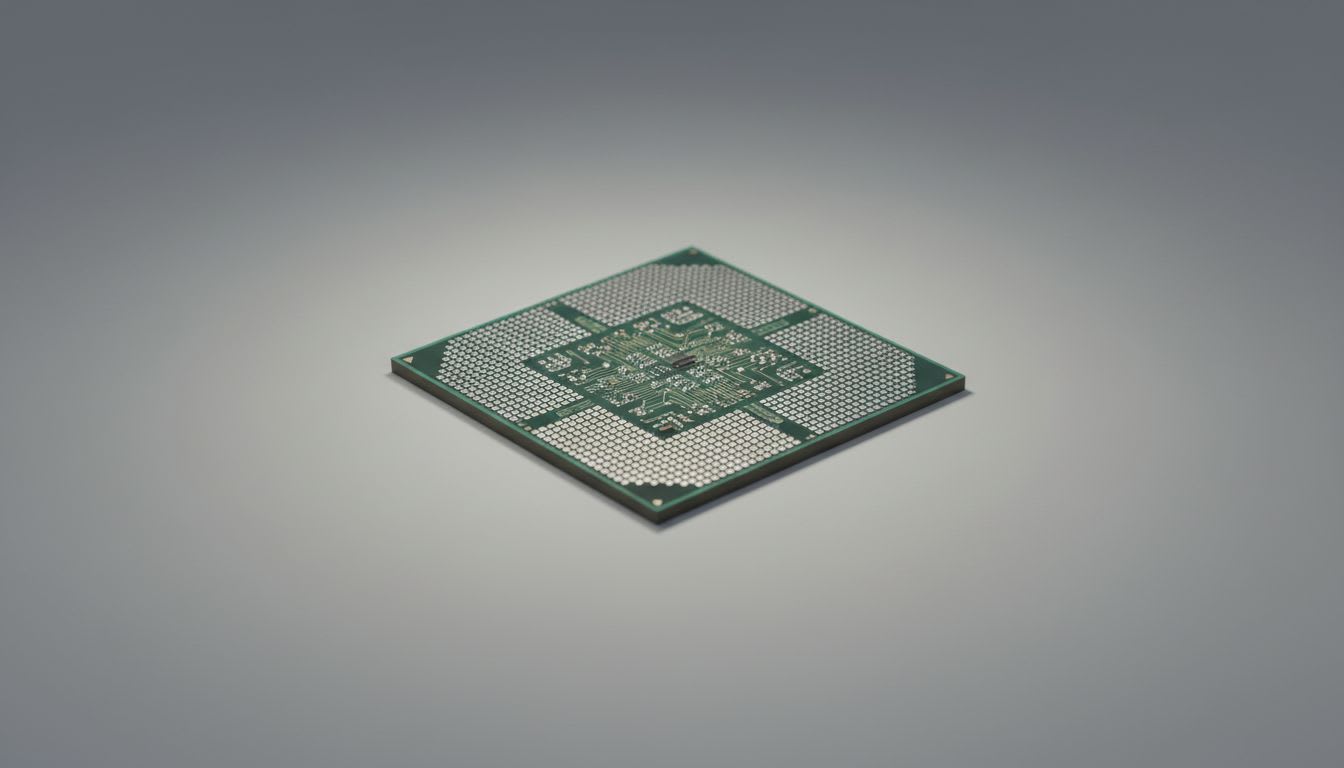
    A process scene in which a wafer surface is finely ground using a diamond wheel

    How the grinding process determines flatness

    The grinding process is a key step that determines the thickness and surface flatness of semiconductor dies. Unlike general cutting processes, precision grinding uses a diamond wheel to remove material in micron units while achieving the desired thickness and flatness at the same time. The tolerance achievable through precision grinding is around ±0.001~0.005mm, and surface roughness reaches Ra 0.2~0.8μm. This is 5~10 times more precise than general CNC milling.

    These figures matter not simply because they show how precise the process is, but because that precision directly determines the bonding quality of the subsequent bonding process. Grinding equipment that combines a high precision stage with a diamond wheel must be able to maintain thickness uniformity even in high speed processing. It is also important to have a configuration that allows flexible selection between fully automatic and manual types depending on the nature of the production line. Huvics PKG Grinder is designed to uniformly process various package types such as FCBGA, WLCSP, and QFN down to the thickness required by the customer. Choosing a grinding machine also means deciding the precision level for the entire process.
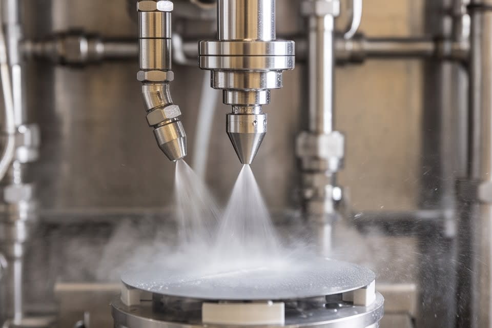
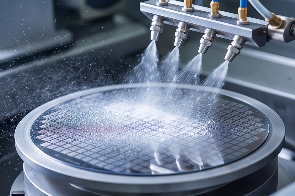
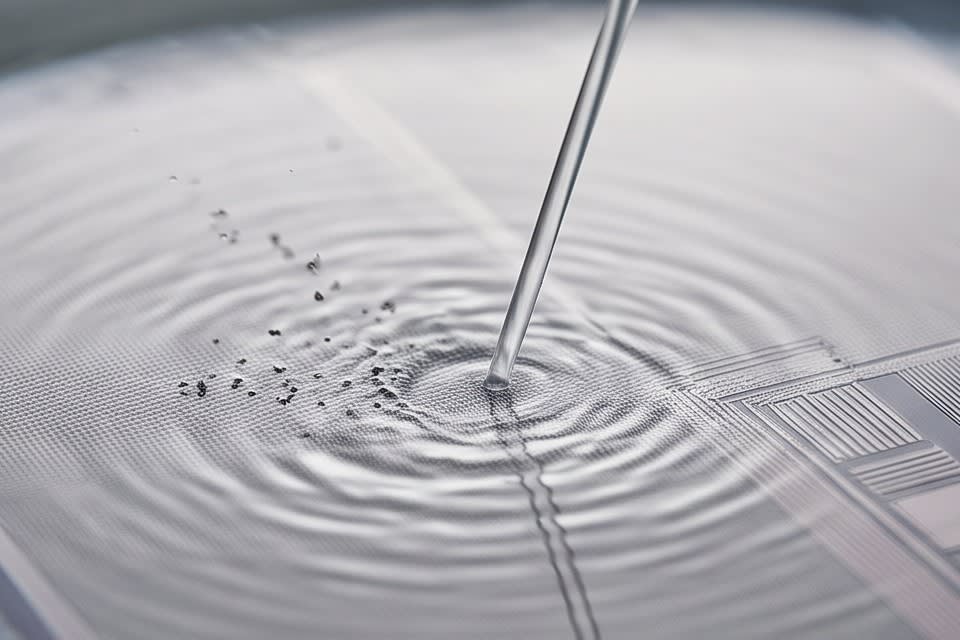
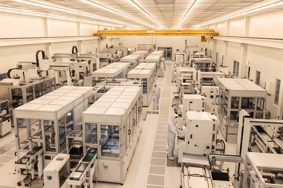
    A process of washing the die surface immediately after grinding by spraying cleaning liquid through a precision nozzle

    Why cleaning after grinding must be treated as one integrated step

    The die surface after grinding is in its most vulnerable state during the process. If fine particles and residues generated during grinding remain on the surface, they can lead to bonding defects in subsequent bonding or packaging steps.

    According to technical data from MSP/TSI, particle removal efficiency in the cleaning process is determined by multiple factors such as cleaning time, temperature, chemical concentration, and agitation method. How precisely these variables are controlled determines final quality. Simply rinsing with water makes it difficult to effectively remove residual particles at the submicron level.

    Huvics cleaning system uses a multi stage method that combines micro bubbles, water jets, and an air knife to remove surface contamination particles step by step, and its oven drying function handles residual moisture after cleaning. When analyzing the process of a customer who came with a camera module defect rate issue, repeated residual particles were occurring because the agitation conditions in the cleaning step had not been optimized. In semiconductor tray cleaning as well, the key was to design different cleaning conditions according to complex contamination types. This is exactly why how a surface precisely processed by grinding is finished in the cleaning step can completely change the value of the process.
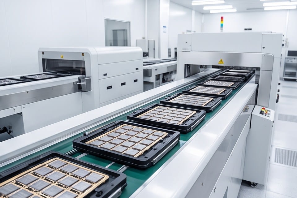
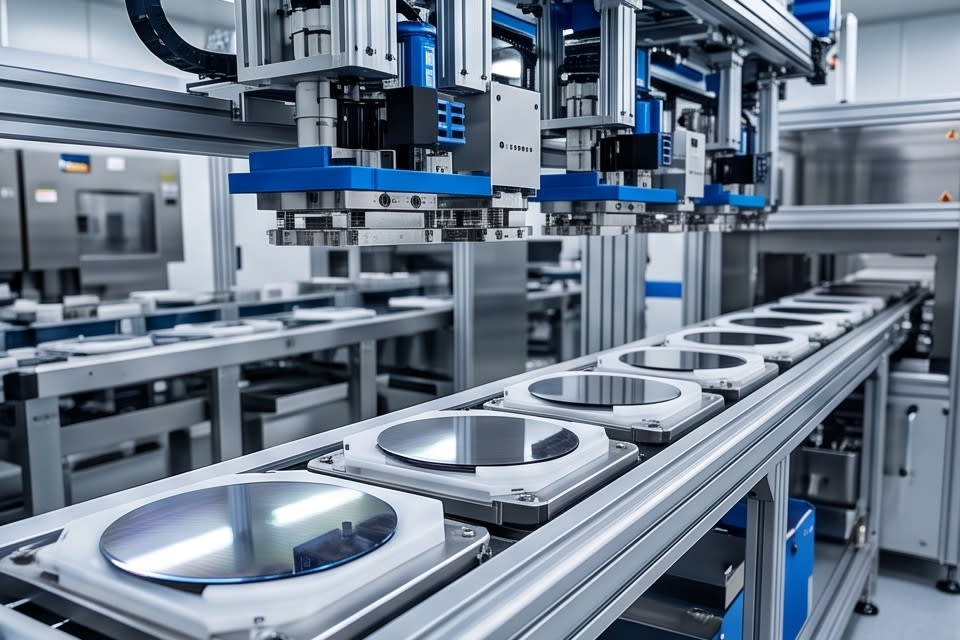
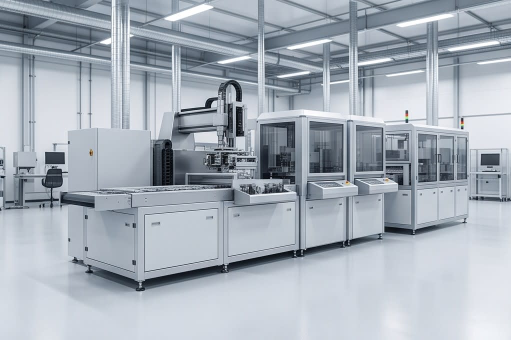
    Automated semiconductor process equipment organically connected along a conveyor belt

    The precision of the stacked structure required by AI semiconductors cannot be completed by the performance of grinding equipment alone. Only when cleaning can fully preserve the flatness created by grinding do those numbers truly have meaning. The two processes must be designed as one continuous flow. That is the real standard that determines packaging quality.


    Huvics is an advanced technology company that develops and manufactures automation equipment and
    production systems across the semiconductor, LED, Mobile, and Cosmetic industries.
    With top talent and continuous technological innovation, we support customers in improving productivity and
    securing quality competitiveness.

    Huvics Contact

    Phone: 031-374-8285
    Email: cdpark@huvics.com

    Huvics Inquiry

  • Why Semiconductor Packaging Reliability Must Be Managed Step by Step from Grinding to Cleaning

    Why Semiconductor Packaging Reliability Must Be Managed Step by Step from Grinding to Cleaning

    Cross sectional structure of high performance semiconductor chips stacked vertically in multiple layers

    It is time to move beyond the idea that shaving a few more micrometers off the thickness of a semiconductor package will not change its performance. As demand for AI semiconductors and high performance memory grows explosively, stacked packaging that vertically stacks dozens of chips has become common, and a single thickness variation has become a factor that can shake the reliability of the entire process. This may sound exaggerated, but when you examine the defect data accumulated in actual manufacturing sites, it is far from an empty claim. Let us take a closer look at how equipment operation becomes the starting point of quality.

    Measurement equipment precisely inspecting semiconductor wafer thickness variation and uniformity

    Why Thickness Uniformity Determines Packaging Reliability

    In high performance semiconductor packaging, thickness uniformity is not optional. In a structure where chips are stacked in multiple layers, even a slight deviation in the thickness of each layer can create voids at the joints or concentrate stress at specific points during subsequent bonding or stacking processes. This phenomenon is not easily noticeable at first, but over time it seriously reduces electrical reliability.

    The concept of total thickness variation, or TTV, reveals this issue numerically. This is why international standards define the allowable TTV range for advanced applications at ±2 to 5 micrometers. As package types become more diverse, such as FCBGA, WLCSP, and QFN, the required machining precision becomes even higher. On manufacturing sites, allowable deviations vary by package type, and process conditions are adjusted in detail. Ultimately, the stability of the packaging process depends on how uniformly thickness can be maintained.

    Grinding equipment processing wafer thickness in micrometer level control

    How Grinding Equipment Operation Determines TTV Stability

    The way grinding equipment achieves TTV stability lies in the combination of mechanical precision and process design. Spindle speed, the material and grit size of the grinding wheel, and the leveling precision of the stage must work together to enable uniform machining at the micrometer level. In the industry, grinding equipment spindles are known to operate in the range of 5,000 to 60,000 RPM depending on the application and material, and selecting the appropriate speed within this range directly affects yield.

    Huvics PKG Grinder combines a high precision stage with a diamond wheel to deliver stable grinding within this range. With Full Auto A Type, B Type, and Manual Type options, line configurations can be selected flexibly, allowing the process to be designed differently according to production scale or product characteristics. The level of automation selected affects the production efficiency of the entire line, and reducing operator intervention also reduces sources of variation. Controlling TTV within specification at the grinding stage is how the foundation is prepared for all subsequent processes.

    Cleaning process spraying liquid onto the wafer surface to remove fine residues

    Why the Cleaning Process Is the Final Gateway to Packaging Quality

    Even after grinding is completed, the risk factors in the packaging process do not disappear. If fine particles and machining residues generated during grinding remain on the surface, they can lead to bonding defects or contamination in later processes. Particle Removal Efficiency, or PRE, is an indicator of how effectively a cleaning system removes surface contaminants. As device structures become finer, even very small particles can affect performance, making it increasingly important to achieve high PRE.

    In the post grinding cleaning process, it has been confirmed that controlling the pressure of the buffing disk and the flow rate of chemical solutions is effective in improving PRE. Huvics Cleaner System adopts a multi step cleaning method that sequentially applies micro bubbles, water jet, and air knife, and adjusts cleaning conditions according to products with various forms and materials, including camera modules, sensors, VCM motors, and trays. It also includes an Oven Dry function, enabling the process from cleaning to drying to be handled in one continuous flow. Managing the connected process from grinding to cleaning and drying in an integrated way, rather than separating each step, is becoming a key trend for improving packaging quality stability.

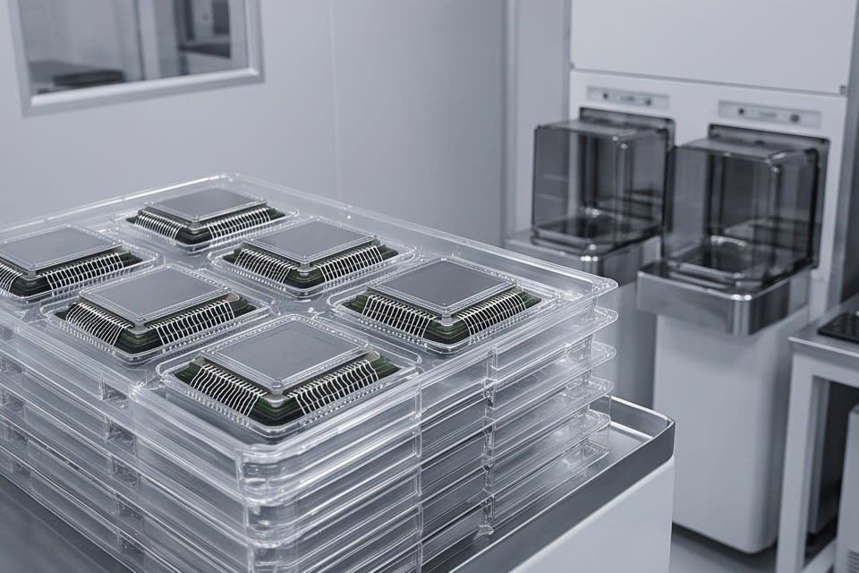
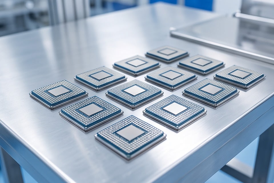
    Semiconductor packages processed with uniform thickness and clean surfaces and aligned on a tray

    Only when grinding precision and cleaning efficiency work together can the reliability of the packaging process truly be secured. Controlling thickness variation at the micrometer level and completely removing contamination particles generated during that process are quality standards for high performance packaging. The fact that the way equipment is operated directly determines the reliability level of the product prompts us to reconsider the standards by which processes should be designed and managed.


    Huvics is an advanced technology company that develops and manufactures automation equipment and
    production systems across the Semiconductor, LED, Mobile, and Cosmetic industries.
    With outstanding talent and continuous technological innovation, we support customers in improving productivity and
    securing quality competitiveness.

    Huvics Contact Information

    Phone: 031-374-8285
    Email: cdpark@huvics.com

    Contact Huvics

  • Precision Grinding and Multistage Cleaning Core Principles That Determine Stacked Packaging Reliability

    Precision Grinding and Multistage Cleaning Core Principles That Determine Stacked Packaging Reliability

    View of multilayer stacked semiconductor packages arranged in rows

    Just a few years ago, thickness control in semiconductor packages was measured by whether they were thin enough. But as AI semiconductors and high-performance memory have become mainstream, the more important question has shifted to how uniform they are. As structures that stack chips in multiple layers have become common, even a single thickness deviation has emerged as a variable that can undermine the reliability of the entire package. As stacked structures become more complex, precision machining and cleaning technologies will become even more decisive standards for process quality.

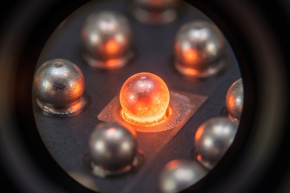
    View of solder microbumps placed inside a semiconductor package

    Why Thickness Uniformity Is a Key Quality Variable in Stacked Packaging

    In 3D IC packaging structures where chips are stacked vertically, thickness uniformity is not simply a dimensional issue. The solder microbumps that connect the chips between each layer repeatedly contract and expand during thermal cycling, and if there is variation in chip thickness, the stress distribution concentrated on the bumps changes. According to research published on ScienceDirect, thermal cycling tests of 3D IC packaging showed that creep in solder microbumps, plastic deformation caused by high-temperature load, can increase by up to 50%, directly affecting thermomechanical reliability.

    The greater the thickness deviation, the more stress becomes concentrated on specific bumps, and package warpage also worsens. As the number of stacked layers increases, the allowable tolerance range for each layer inevitably becomes narrower. When thickness nonuniformity in a single chip accumulates, the flatness of the entire package collapses, leading to bonding defects or electrical shorts in subsequent processes. In the end, thickness variation may not be visible, but it appears directly in the reliability metrics of the final product. As stacked packaging advances, securing thickness uniformity is becoming the starting point of process quality.

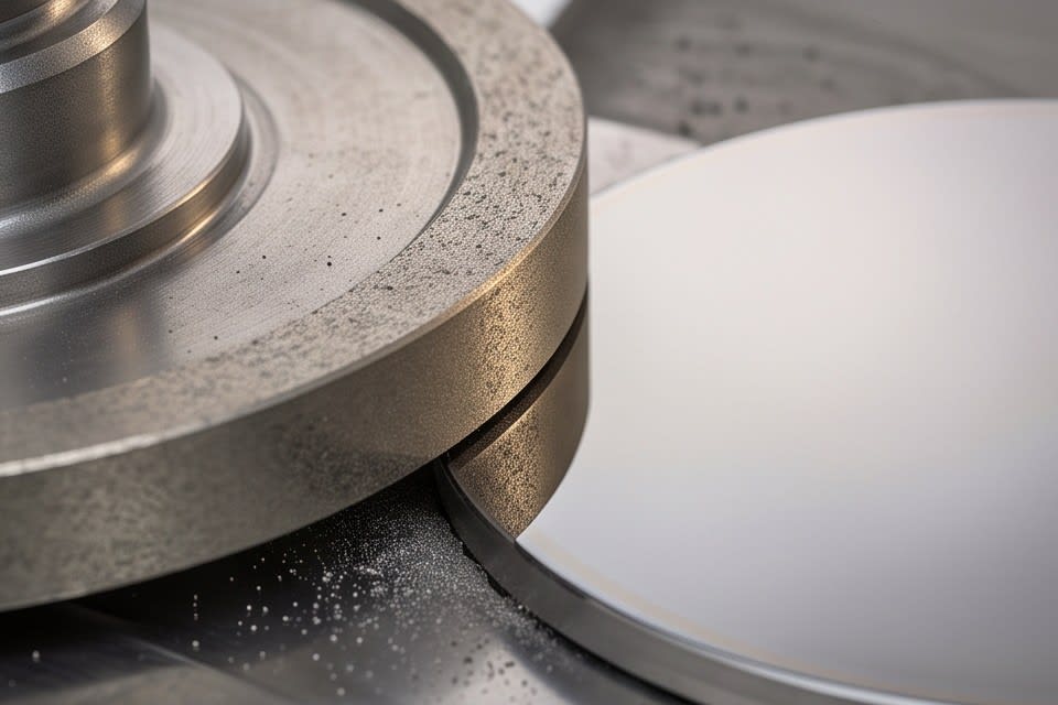
    View of a wafer or chip thickness being precisely machined using a diamond wheel

    Limitations of Conventional Machining Methods and the Role of Precision Grinding Technology

    Conventional grinding and chemical mechanical polishing have long been used as standards in semiconductor thinning processes, but their limitations are clear at the level of precision required by advanced packaging. According to an analysis by Eureka PatSnap, conventional grinding and chemical mechanical polishing processes often exceed thickness deviations of ±2μm, falling short of the latest package specifications that require submicron precision. As package types become more diverse, such as FCBGA, WLCSP, and QFN·DFN, and target thickness values vary, it is difficult for a single method to handle all specifications with the same level of precision.

    The moment deviation exceeds ±2μm, the package fails to meet the flatness criteria required in the next process, directly leading to yield loss. Micron-level grinding that combines a high-precision stage with a diamond wheel is one approach to closing this gap, and the same analysis shows that it can reduce material waste by 15 to 30% compared with conventional methods. Equipment such as a PKG Grinder, which supports both fully automatic and manual configurations, is designed to secure stable thickness precision in high-speed processes while maintaining production line flexibility. More important than which method is chosen is first defining the target package specification and allowable tolerance, then selecting the machining method that fits them.

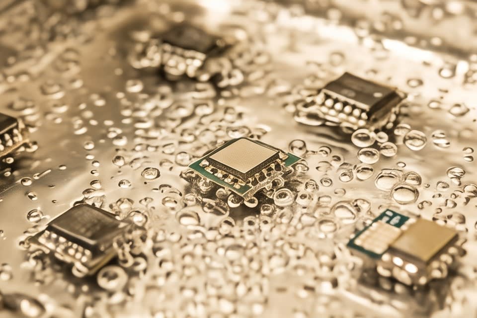
    View of fine water droplets formed on the surface of a semiconductor chip

    How the Cleaning Process Determines Final Quality

    If precision machining reduces thickness variation, the cleaning process determines the surface condition before the result moves on to the next stage. For components that require ultra-precision optical and electrical characteristics, such as camera modules or autonomous driving sensors, even a single fine particle left after grinding can result in a defect judgment. In the field, cleaning is often regarded as the last step, but in practice it is the process that determines final quality.

    According to research published in MDPI, cleaning solutions containing micro-nano bubbles improve the photoresist removal rate by 30%. A multistage cleaning method that applies Micro Bubble, Water Jet, and Air Knife step by step is structured to separate and discharge contaminant particles at each stage that are difficult to remove with a single method. For parts with complex shapes, such as VCM motors or semiconductor trays, the combination and sequence design of cleaning methods directly affect removal efficiency. When residual moisture is also removed through the Oven Dry process after cleaning, the possibility of secondary contamination in subsequent assembly or inspection processes is reduced.

    Lower defect rates and stable yield ultimately come from how precisely the surface is controlled at this cleaning stage. The fact that invisible particles determine the quality of the entire process becomes clear the moment cleaning results are connected to shipping quality.

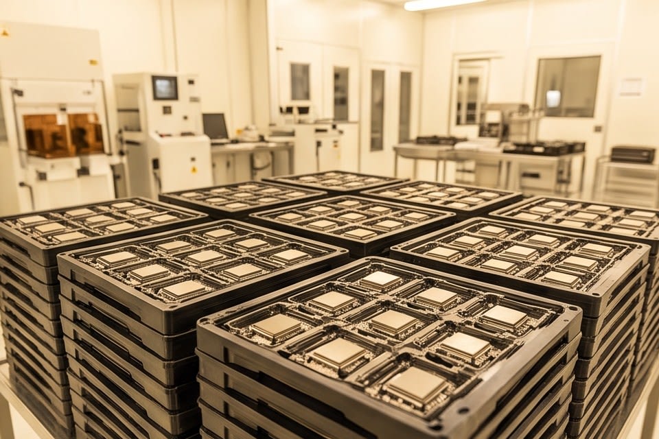
    View of cleaned semiconductor components aligned and loaded on trays

    Reducing defects in semiconductor processes is not a matter of just one step. Package reliability is secured only when two processes work together: precision grinding that controls thickness variation at the micron level, and multistage cleaning that removes surface contaminant particles step by step. In a structure where the precision of each individual process determines the yield and reliability of the final product, which technologies are selected and how they are combined become practical benchmarks of manufacturing competitiveness.


    Huvics is an advanced technology company that develops and manufactures automation equipment and
    production systems across the semiconductor, LED, Mobile, and Cosmetic industries.
    With top talent and continuous technological innovation, we help customers improve productivity and
    secure quality competitiveness.

    Huvics Contact

    Tel: 031-374-8285
    Email: cdpark@huvics.com

    Huvics Inquiry

  • Why Grinding and Cleaning Process Design Learned from Camera Module and Sensor Production Lines Changes Yield

    Why Grinding and Cleaning Process Design Learned from Camera Module and Sensor Production Lines Changes Yield

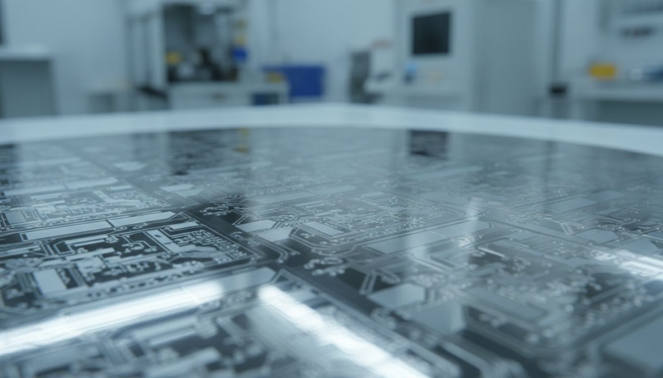
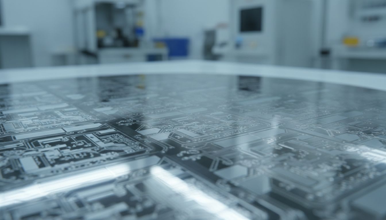
    The glossy and reflective surface of a semiconductor wafer placed on high-precision equipment.

    If you discover too late that a thickness deviation of only a few micrometers has occurred during the grinding process, yield loss and rework costs in downstream processes may already have accumulated. Thickness nonuniformity undermines the reliability of the entire chip stacking structure, and once the package is completed, it can lead to defects that are difficult to reverse. If this issue is left unaddressed, it can spread to delivery delays and customer claims, making precise thickness control essential from the very beginning of the process.

    A fine stacked structure of vertically layered semiconductor chips and a cross section of the internal circuits.

    Why Thickness Uniformity Matters in Chip Stacking Packaging

    As semiconductor packaging technology evolves into 3D stacked structures, maintaining uniform thickness in each chip has emerged as a key factor that determines overall package performance. In structures where multiple chips are stacked vertically, such as high-bandwidth memory, narrower gaps between chips improve signal transmission quality. However, even a slight thickness deviation increases the risk of bonding defects and warpage.

    Across the industry, advanced stacked packaging is moving toward wafer thickness targets in the range of 25 to 50 micrometers. This is less than half the thickness of a human hair, requiring a level of precision that cannot even be verified with the naked eye.

    As package formats become more diverse, including FCBGA, WLCSP, and QFN/DFN, the thickness standards and tolerances required for each structure also vary. This is why target thickness and machining strategies must be set differently depending on the package type, even within the same grinding process. Ultimately, securing thickness uniformity in chip stacking packaging is not simply a matter of machining precision. It has become a process design issue that determines product reliability and overall yield.

    A machining scene where a diamond wheel grinds the wafer surface and fine particles scatter.

    How the Grinding Process Determines Thickness Uniformity

    The performance of grinding equipment is evaluated mainly by two factors. One is machining precision, and the other is process stability. A grinding method that combines a high-precision stage with a diamond wheel enables thickness control at the micron level and is advantageous for maintaining uniform flatness across the entire wafer surface.

    In WLCSP structures, wafer grinding becomes the core method for reducing the overall package height. In FCBGA structures, the target thickness must be set differently because the package takes advantage of its greater thickness and lower conduction loss. This is why grinding strategies must differ by package type.

    To maintain stable quality even in high-speed process environments, the automation level of the equipment becomes an important variable. The Huvics PKG Grinder supports both Full Auto and Manual configurations, allowing flexible response according to the production line type and required yield. The manual method is suitable for low-volume and high-mix production, while the automated method offers strong advantages in minimizing process variation in mass production environments.

    The key to yield stability lies in which equipment configuration is selected for the grinding process and how precisely the machining conditions are set for each package type.

    A cleaning process in which liquid sprayed from a nozzle removes contaminants from the wafer surface.

    Why the Cleaning Process After Grinding Determines Final Quality

    The process is not complete even after grinding is finished. If fine particles and surface contaminants generated during grinding are not removed, they become the source of defects in subsequent processes. In manufacturing sites for ultra-precision components such as camera modules and sensors for autonomous driving, where even a single speck of dust is hard to tolerate, companies repeatedly experience yield collapse the moment the cleaning step is omitted. If contaminant particles remain on the bonding surface, they lead to poor electrical contact, and in optical components, they directly cause image quality degradation.

    A multistage cleaning method that combines microbubbles, water jets, and air knives step by step removes fine contamination on the product surface in different ways at each stage, securing higher particle removal efficiency than a single cleaning method. After cleaning, a drying process must follow to completely remove residual moisture, and equipment integrated with an oven drying function can handle these two steps within one continuous flow.

    Huvics has applied solutions tailored to different contamination conditions and cleaning requirements at each site, including cases involving semiconductor tray cleaning and camera module defect improvement. Since cleaning conditions vary depending on product type and process environment, reviewing both equipment flexibility and site suitability leads to practical quality improvement.

    A wafer moving automatically along a conveyor system while undergoing a precision process.

    As chips become thinner and stacked structures become more complex, actual yield is determined not only by the precision of grinding and cleaning individually, but by how consistently the two processes are connected as one continuous flow. Minimizing thickness deviation in the initial grinding stage and then finishing the process without contamination in the cleaning stage, only when these two conditions are met together can package reliability be secured. Improving each process individually is not enough. It is necessary to consider the entire flow from grinding to cleaning together from the process design stage.


    Huvics is an advanced technology company that develops and manufactures automation equipment and
    production systems across the semiconductor, LED, Mobile, and Cosmetic industries.
    With top talent and continuous technological innovation, we support customer productivity improvement and
    quality competitiveness.

    Huvics Contact Information

    Phone: 031-374-8285
    Email: cdpark@huvics.com

    Contact Huvics

  • Are You Properly Managing the 2 Key Processes That Determine Semiconductor Packaging Yield

    Are You Properly Managing the 2 Key Processes That Determine Semiconductor Packaging Yield

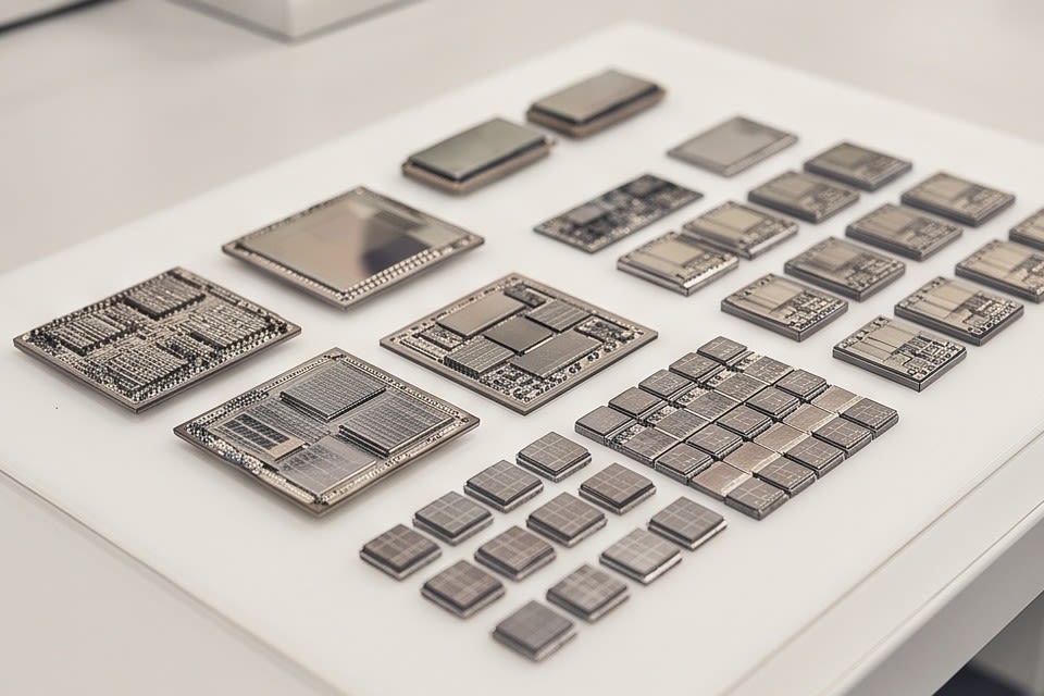
    Semiconductor package samples arranged in various sizes and shapes

    In the semiconductor industry, ‘packaging’ was long regarded as a finishing step placed behind design and process work. However, as demand for AI accelerators and high-performance memory has surged, the situation has changed rapidly. Product competitiveness now depends not only on the performance of a single chip, but on how precisely multiple chips are stacked and connected. Packaging technology now stands at the center of a technology race as intense as semiconductor design itself.

    A diamond wheel uniformly grinding the surface of a semiconductor wafer

    Why Ultra-Precision Grinding Determines Yield

    High-bandwidth memory used in AI accelerators must process more than 1TB of data per second through a vertically stacked structure. To meet this requirement, each stacked chip must have uniform thickness, and surface flatness must also be controlled at the micron level. According to Mordor Intelligence, 3D stacked memory accounts for 34.28% of revenue share in the advanced semiconductor packaging market as of 2025, establishing itself as the leading technology.

    As package formats diversify, such as FCBGA, WLCSP, and QFN, thickness precision standards also vary by type. For example, WLCSP requires a fine pitch between 0.3mm and 0.5mm. Ultimately, grinding precision in the packaging process is a key variable that determines yield. Even a slight increase in thickness variation can undermine the electrical reliability of the entire stacked structure, directly leading to performance degradation in the final product.

    Huvics PKG Grinder responds to these standards with micron-level grinding using a diamond wheel. It is available in both Full Auto and Manual configurations, allowing flexible application according to the production line structure of each customer, while maintaining stable quality even in high-speed processes to achieve high yield. Machining precision is product reliability is the principle that most clearly explains the role this equipment plays in semiconductor packaging processes.

    A cleaning process that sprays liquid onto a semiconductor surface to remove contaminant particles

    Why the Cleaning Process Is the Starting Point of Quality

    If grinding determines the form of packaging, cleaning is the process that ensures this form can perform its intended function. A single fine particle remaining on the semiconductor surface can contaminate the entire subsequent process or lead to defects in the final product. Especially in components that require optical precision, such as camera modules or autonomous driving sensors, invisible contamination can quietly erode product reliability. This is why the cleaning process must be treated not as simple washing, but as the starting point of quality stability.

    Huvics Cleaner System removes contaminant particles from product surfaces by sequentially combining Micro Bubble, Water Jet, and Air Knife, and consistently handles the drying process through its Oven Dry function. Cleaning conditions can be configured differently according to product types such as camera modules, sensors, VCM motors, and trays, enabling a single system to address diverse process requirements.

    In practice, many cases have shown that defects occurring in semiconductor tape bonding processes and yield loss in camera modules can be resolved by improving the cleaning process. Reducing particles reduces defects, and reducing defects increases yield. Engineers who have worked with cleaning processes know well how difficult it is to implement this simple connection in the field. The significance of precision cleaning is confirmed by the fact that it is not the end of the process, but the foundation of quality.

    Precisely processed semiconductor packages arranged in a row

    The competition in semiconductor packaging technology is now shifting toward process precision as much as chip design. Grinding and cleaning are the two pillars that support yield and reliability in this competition. If either one becomes unstable, even the most sophisticated package design will struggle to deliver its intended performance in the field. In an era when technological precision becomes product competitiveness, how firmly each and every process is built will ultimately determine a company’s position in the future semiconductor market.


    Huvics is an advanced technology company that develops and manufactures automation equipment and
    production systems across the semiconductor, LED, Mobile, and Cosmetic industries.
    With top talent and continuous technological innovation, we support customers in improving productivity and
    securing quality competitiveness.

    Huvics Contact

    Tel: 031-374-8285
    Email: cdpark@huvics.com

    Contact Huvics

  • Core Competitiveness in Advanced Semiconductor Packaging – Huvics PKG Grinder Ultra-Precision Grinding Solution

    Core Competitiveness in Advanced Semiconductor Packaging – Huvics PKG Grinder Ultra-Precision Grinding Solution

    Huvics

    The advanced semiconductor packaging market has become a stage for more intense technological competition than ever before. Today, the value of semiconductors is determined not only by how far they can push performance limits, but also by how thinly and precisely they can be packaged. In particular, thickness uniformity and high flatness, which are required in fine processes, have become essential indicators for securing a technological edge.

    The Importance of Ultra-Precision Grinding Processes

    In the production of next-generation artificial intelligence and high-performance memory semiconductors, the perfection of the grinding process that ensures physical reliability has become a decisive factor that determines the fate of the final product. In response to these demands of the times, Huvics is presenting a new industry standard through its ultra-precision grinding solution, PKG Grinder. Going beyond simply manufacturing machines, Huvics is becoming a reliable partner for companies seeking to overcome technological limits by helping them address the subtle differences found in semiconductor manufacturing sites.

    Precision process in a semiconductor cleanroom

    Technical Strengths of the PKG Grinder

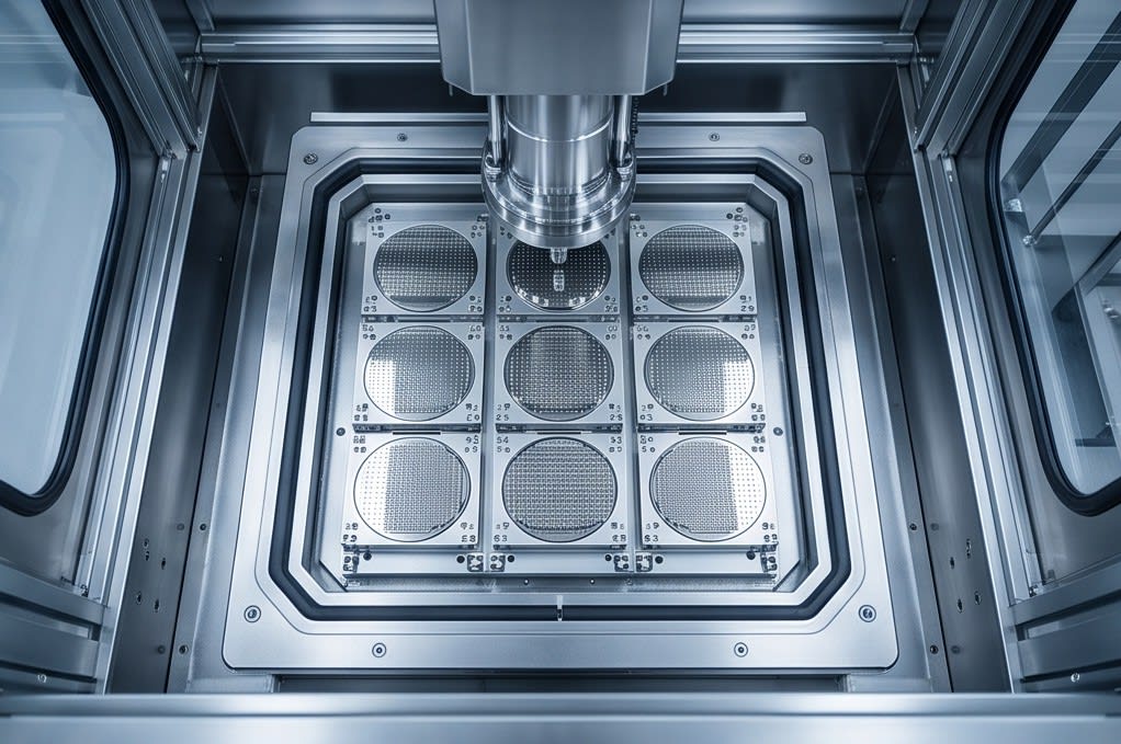
    The greatest strength of the Huvics PKG Grinder lies in the perfect combination of a high-precision stage and advanced diamond wheel technology. This technology, which does not allow even the slightest error during the grinding process, delivers precise grinding at the micron level. When performing advanced package processes such as flip chip ball grid array or wafer-level chip-scale package, maintaining unwavering flatness is essential to maximizing the physical reliability of the product.

    Semiconductors produced with this equipment can maintain consistent performance even under changing external environments or high-speed operating conditions. This improves the durability and efficiency of the products customers bring to market, ultimately leading to a noticeable enhancement in the quality of technology experienced by end users.

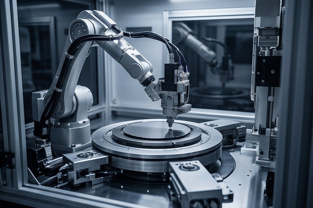
    Operation of an ultra-precision robotic arm

    Customized Production Lineup and Strategy

    Requirements on the production floor vary from company to company. Huvics provides a broad lineup that reflects diverse production scales and characteristics.

    • Support for high-speed automation systems for mass production
    • Detailed control with manual types for special purposes
    • Strategic equipment selection directly connected to production yield
    • Stable quality maintenance in a rapidly changing market environment

    Front view of PKG Grinder equipment

    Technological Competitiveness and Sustainable Growth

    We are now in an era where the precision of equipment directly becomes a company’s competitiveness. The customized solutions from Huvics are not merely auxiliary tools that improve efficiency, but practical weapons that help companies stay one step ahead in global technology competition. By deeply understanding the challenges experienced engineers face in the field and incorporating those insights into equipment design and operation methods, companies can maximize process efficiency.

    The ability to obtain high-quality results that remain stable even in high-speed production environments gives companies the technical confidence they need to advance into broader markets. As a result, this technological support provided by Huvics will drive sustainable corporate growth and become a key force in securing stable market share and product reliability in the advanced semiconductor packaging market.

    In the fierce technological competition to break through the limits of semiconductor packaging, what we must ultimately focus on is how precisely the finest details of the process can be controlled. The Huvics solution, which maximizes the physical reliability of products through ultra-precision grinding technology, goes beyond being a tool for improving efficiency and will become a key driving force for securing unwavering competitiveness in a rapidly changing market environment. Now that small differences in processes are coming together to define the standards of future technology, we invite you to add the most accurate and robust technological answer to your production site with Huvics.


    Huvics is an advanced technology company that develops and manufactures automation equipment and
    production systems across the semiconductor, LED, mobile, and cosmetics industries.
    With top talent and continuous technological innovation, we support customers in improving productivity and
    securing quality competitiveness.

    Contact Huvics

    Phone: 031-374-8285
    Email: cdpark@huvics.com

    Huvics Inquiry

  • Huvics’ Ultra-Precision PKG Grinder Technology Philosophy That Elevates Semiconductor Packaging Quality

    Huvics’ Ultra-Precision PKG Grinder Technology Philosophy That Elevates Semiconductor Packaging Quality

    Huvics

    In semiconductor packaging processes, micron-level deviations are more than simple numerical differences. They often become critical variables that determine the quality and reliability of the final product. As the markets for artificial intelligence and high-performance memory semiconductors grow rapidly, manufacturing sites demand even greater thickness uniformity and flatness. However, maintaining these qualities without compromise amid increasingly complex processes is never easy.

    How can we secure outstanding yield by overcoming technical limits in a demanding production environment filled with countless variables? Let us explore the answer through the technology philosophy of Huvics, which is redefining the standard of ultra-precision with the unwavering belief that small differences create premium quality.

    High-precision stage and grinding head of the PKG Grinder

    Ultra-Precision Solutions for Next-Generation Semiconductor Processes

    In the advanced semiconductor packaging market, achieving ultra-precision has now moved beyond simply proving numerical performance. It has become the most important measure that determines the reliability of the final product, and an era has arrived in which invisible microscopic deviations can decide the success or failure of an entire process. In response to these industry demands, Huvics realizes exceptional detail through PKG Grinders optimized for next-generation semiconductor processes.

    Quality Completed with High-Precision Technology

    In complex packaging processes that require highly advanced technologies, such as FCBGA and WLCSP, even micron-level deviations can have a critical impact on quality. Huvics equipment perfectly combines high-precision stage technology with diamond wheel technology to ensure strict thickness uniformity and flatness even under extreme conditions. The unwavering technology philosophy of Huvics, where even the smallest detail defines product completeness, becomes the driving force that maintains stable high yield regardless of the production environment.

    The Distinctive Technical Advantages Unique to Huvics

    The core of the perfect detail realized by Huvics begins with the sophisticated harmony between high-precision stages and advanced diamond wheel technology. These two key technologies are organically integrated to thoroughly suppress unnecessary vibration and consistently maintain stable processing performance even in demanding high-speed rotational process environments. The differentiated strengths pursued by Huvics are as follows.

    • Not remaining satisfied with simply improving mechanical precision
    • Securing process stability directly connected to production site efficiency
    • Maximizing yield through persistent focus on technical sophistication

    Precisely aligned semiconductor packages

    Site-Customized Process Optimization Solutions

    The true perfection pursued by Huvics is completed not merely through standardized equipment specifications, but through a deep understanding of each customer’s production scale and complex site conditions. We propose optimized customized solutions tailored to the nature and scale of each process, from fully automatic systems to manual types, and refine every design detail so that consistent high performance can be delivered in any production environment.

    The Role of a Trusted Technology Partner

    This flexible approach is the key driving force that has positioned Huvics not only as an equipment supplier, but also as a trusted technology partner that considers the sustainable growth of its customers. Careful configuration that does not overlook even the smallest variable on the production floor ensures unwavering process stability even in mass production systems, providing reliable support so that every process customers face can achieve perfection.

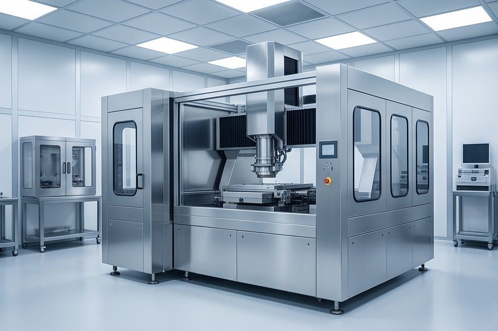
    PKG Grinder installed in a cleanroom

    Technical Persistence Leading Future Industries

    The pace of semiconductor technology evolution is accelerating every day, and accordingly, the precision standards required by manufacturing sites are constantly being renewed. Even amid this flow of change, Huvics prepares for the future of the industry through unwavering technical persistence. Our equipment is not simply a collection of hardware, but a technology-intensive result completed through countless trials, errors, and research efforts.

    Continuous Innovation and Quality Improvement

    From high-performance memory semiconductors to AI-based complex packaging, our ability to deliver the best results in any process comes from the experience we have accumulated and our passion for detail. Customers choose Huvics because of the clear difference in quality revealed in the final results, and we continually examine every stage of the process in detail to never fall short of those expectations. The steps Huvics takes toward a higher level of precision beyond technological limits will continue to establish new standards in the semiconductor packaging industry and drive advancement across the entire industry.

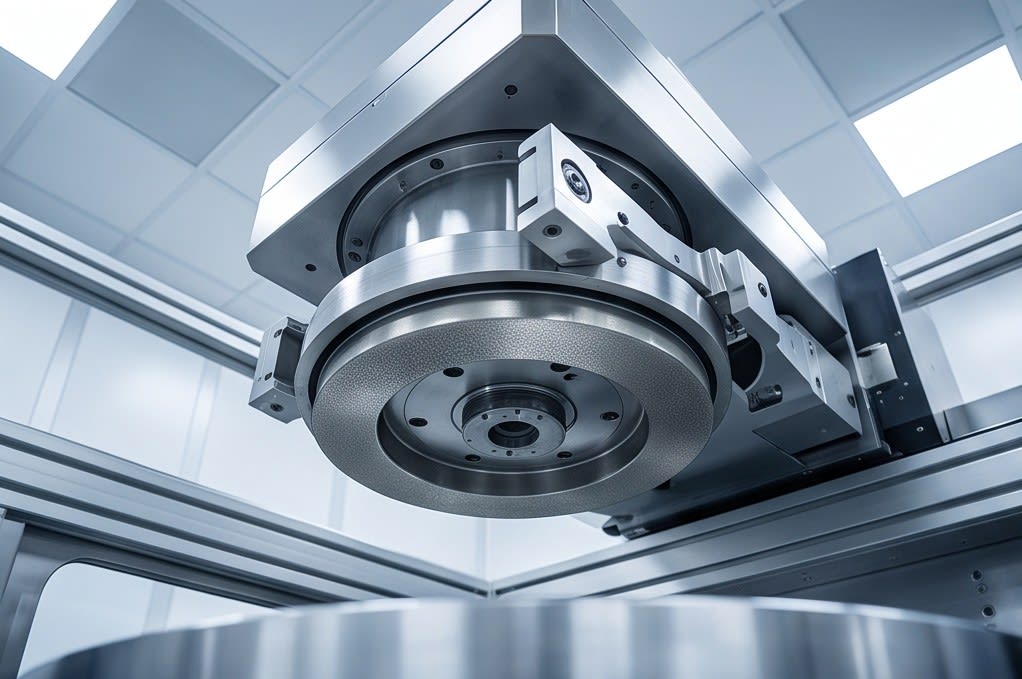
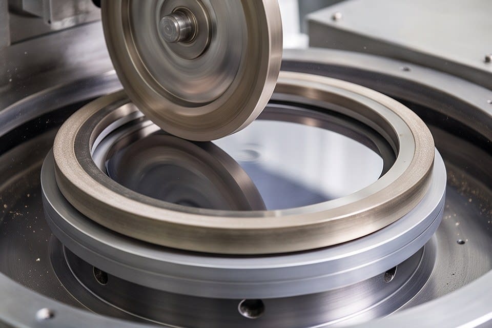
    Diamond wheel section

    Closing

    When facing the challenge of ultra-precision in the semiconductor packaging market, the factor that ultimately determines success or failure is the power of uncompromising detail. The persistent philosophy of Huvics in controlling even micron-level microscopic deviations becomes a reliable technical foundation that goes beyond supplying equipment and helps each customer’s production process lead to results in their most perfect form.

    Just as small differences come together to create truly outstanding products, elevate your semiconductor packaging process to a higher level with the meticulous approach of Huvics, which does not overlook even the smallest variable on site. Huvics will always stand with you on the journey of innovation toward a new standard created by sophistication beyond technological limits.

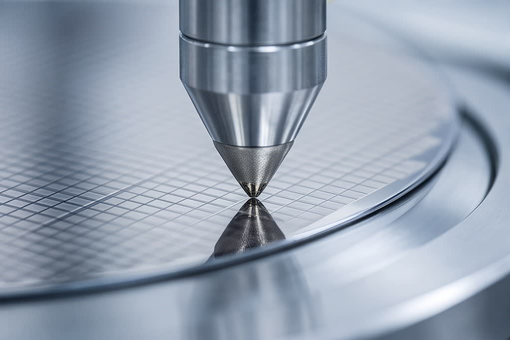
    Precision tip on semiconductor wafer surface


    Huvics is an advanced technology company that develops and manufactures automation equipment and
    production systems across the semiconductor, LED, mobile, and cosmetic industries.
    With top-tier talent and continuous technological innovation, we support customers in improving productivity and
    securing quality competitiveness.

    Huvics Contact

    Phone: 031-374-8285
    Email: cdpark@huvics.com
    Huvics Inquiry

  • Huvics One-Stop Laminator System – A Design Philosophy That Enhances Productivity and Precision in Semiconductor Packaging

    Huvics One-Stop Laminator System – A Design Philosophy That Enhances Productivity and Precision in Semiconductor Packaging

    Huvics

    As semiconductor packaging processes become finer and more complex with each passing day, concerns on the manufacturing floor continue to grow. This is because manufacturers face a dilemma where increasing precision can slow down speed, while pursuing productivity can easily compromise quality stability. Is achieving both of these conflicting goals truly an impossible challenge?

    Now, there is no longer a need to compromise between process bottlenecks and unstable quality. Discover the precise design philosophy behind the innovative one-stop laminator system proposed by Huvics and how it is changing the landscape of complex semiconductor manufacturing environments.

    Overview of the Huvics One Stop System

    Innovation in Semiconductor Packaging, One-Stop Laminator System

    Integrated Process Design and Production Efficiency

    Today, semiconductor packaging processes are becoming increasingly advanced, and manufacturing sites are facing the significant challenge of achieving two conflicting goals at the same time: precision and speed. With technological advancements, semiconductor devices have become smaller and more complex, but the physical limitations of the manufacturing lines that handle them still remain a factor that hinders productivity.

    To overcome this complex process environment head-on, Huvics has designed an innovative one-stop laminator system that integrates tape mounting and ultraviolet (UV) curing technology into a single solution.

    Key Benefits and Competitive Strengths of the System

    The main benefits provided by this system are as follows.

    • Organic connection within a single process from expander to final curing
    • Elimination of segmented steps to resolve product transfer and setup bottlenecks
    • Maximized process stability through LED-based precision ultraviolet curing
    • Reduced semiconductor production takt time and strengthened manufacturing competitiveness

    Precision Handling Robot Head

    User-Centered Precision Control Philosophy

    Work Convenience and Interface Implementation

    Another core pillar of the design philosophy pursued by Huvics is achieving the perfect balance between user convenience and process precision. No matter how outstanding the performance of equipment may be, its efficiency can only be reduced if operators on site cannot control it intuitively.

    Based on this perspective, Huvics has implemented a user-friendly interface that helps on-site operators manage complex semiconductor packaging processes more easily and efficiently. By converting complex technical elements into data and visualizing them, it creates an environment that maximizes the value of precision technology and minimizes the possibility of operator error.

    User Friendly UI Panel

    Precision Ultraviolet Curing and Quality Assurance

    In particular, the LED-based precision ultraviolet (UV) curing technology introduced into the system by Huvics delivers excellent performance in maintaining uniform adhesive strength. In multi-layer stacked packaging processes, even a very small difference in adhesion can determine the quality of the final product, and the Huvics system prevents even the subtle quality deviations that often occur in these processes in advance.

    This precision control capability dramatically removes uncertainty from the work environment and enhances process stability, helping customers achieve consistent results under any conditions. As a result, by integrating advanced technology with a people-centered operating environment, Huvics goes beyond equipment that simply pursues production efficiency and simultaneously realizes the two values of customer quality assurance and productivity improvement.

    This becomes a key strategy that helps semiconductor manufacturing sites move beyond technological complexity and enter a stable growth trajectory.

    LED Precision Curing Module

    A Stable Growth Strategy for the Future

    In increasingly complex semiconductor packaging processes, achieving both productivity and precision is no longer an option but an essential task. Through the innovative solution of the one-stop laminator system, Huvics has secured process connectivity and implemented a user-centered operating environment so that technological advancement does not lead to confusion on site.

    The design philosophy of Huvics, which directly addresses the challenges of complex manufacturing sites, goes beyond simply increasing speed and will serve as a reliable technological foundation that guarantees unwavering quality in any environment. If you are now considering process efficiency, with Huvics, you can move beyond technological complexity and envision a clearer future of stable growth.


    Huvics is an advanced technology company that develops and manufactures automation equipment and
    production systems across the semiconductor, LED, mobile, and cosmetics industries.
    With top-tier talent and continuous technological innovation, we support customers in improving productivity and
    securing quality competitiveness.

    Huvics Contact Information

    Phone: 031-374-8285
    Email: cdpark@huvics.com
    Huvics Inquiry

  • Zero Defect Rate in Semiconductor Packaging, Customized Total Solution

    Zero Defect Rate in Semiconductor Packaging, Customized Total Solution

    Huvics

    In the past, the semiconductor manufacturing industry has focused on improving yields, marking remarkable progress. However, as technology is miniaturized to the nanometer scale, we have entered an era demanding extreme precision towards zero defect rates, where even a single minute error can result in substantial losses. In this rapidly changing environment, true partnerships that go beyond simple equipment supply, by providing deep analysis of the entire process and offering customized solutions along with continuous technical support, have become the key competitive advantage for semiconductor companies. Therefore, the key partnership proposed by Huvics is increasingly crucial for companies striving to achieve zero defect rates in semiconductor packaging processes.

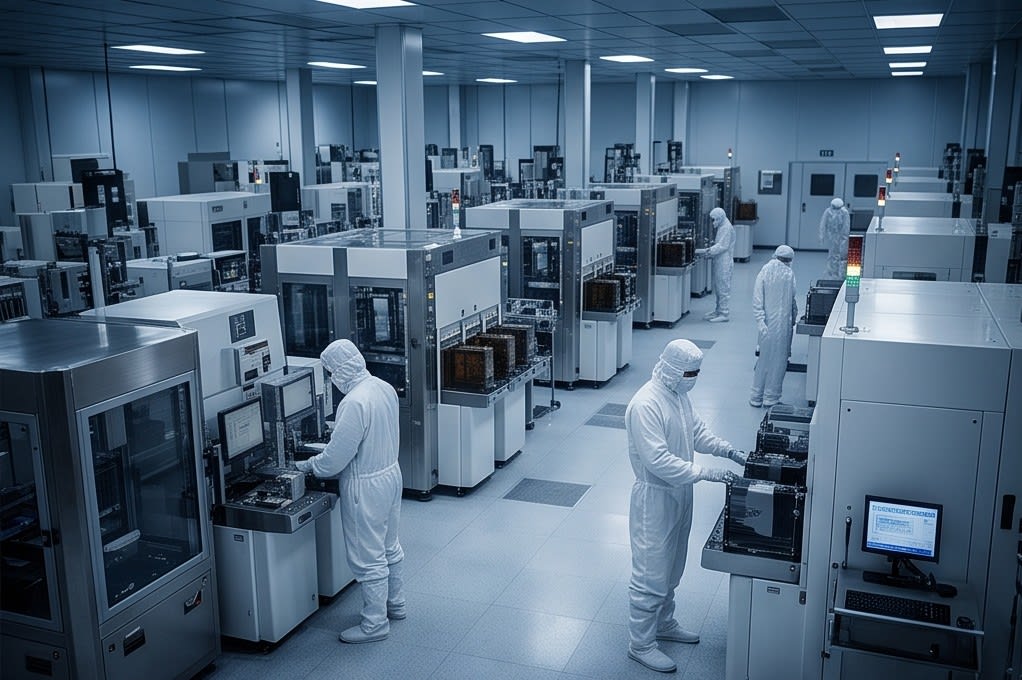
    Smart Factory Cleanroom

    Deep Process Analysis and Problem Identification

    The semiconductor packaging process requires precision at the nanometer level, where even the tiniest error can lead to significant economic losses. For semiconductor manufacturing companies, ‘zero defect rate’ isn’t merely a hope but an absolute goal that determines the survival of the business. Understanding the stringent standards of the industry, Huvics goes beyond simply providing state-of-the-art equipment to offer a differentiated approach by deeply analyzing the entire manufacturing process of client companies. Huvics concentrates the following capabilities to clearly understand the complex and unique challenges faced by clients:

    • Identify potential problems thoroughly from the process design stage
    • Accurately diagnose inefficient process areas
    • Clearly understand the challenges faced by clients

    Like finding the first knot in a complex tangle, solving problems from an in-depth understanding from the initial stages lays a solid foundation for proposing customized total solutions that dramatically lower defect rates and maximize production efficiency. Thanks to this close technical support and in-depth analysis, Huvics has firmly established itself as an indispensable key partner in the successful business journey of leading global companies.

    Refined Microchip

    Customized Total Solution for Increased Production Efficiency

    Based on the aforementioned deep process analysis, Huvics proposes a ‘customized total solution’ that goes beyond simple equipment supply to maximize production efficiency and innovatively reduce defect rates. This is not a superficial approach of merely replacing one or two pieces of equipment. Instead, it means viewing the entire manufacturing process of client companies as an organic system and providing a comprehensive solution by deeply analyzing and optimizing the interaction and flow of each stage.

    For instance, if defects occur repeatedly in a specific process, instead of attributing it solely to the equipment at hand, we diagnose the entire flow considering the possibility of accumulated minute errors from previous processes. The solutions of Huvics can be called a ‘client-customized strategy’ because they are designed to perfectly align with different production environments, product characteristics, and business goals of each client.

    This delicate and customized approach, combined with close technical support, enables Huvics to fundamentally improve the quality and stability of semiconductor packaging processes while realizing the core value of assisting leading global companies in identifying and establishing the optimal production environment based on their deep-seated needs. This makes us the most reliable partner on the journey towards the ultimate goal of zero defect rates.

    Systematic Semiconductor Module

    Close Technical Support for Continuous Success

    Beyond proposing cutting-edge solutions, Huvics regards ‘close technical support’ as its core value and acts as a true partner for the continuous success of client companies. From the critical stages of equipment installation and initial operations to addressing any technical issues that may arise over long-term operations, Huvics provides prompt and professional support. Due to the highly complex nature of semiconductor packaging processes, immediate response to unforeseen issues is absolutely essential to minimize production interruption risks and maintain stable production lines.

    Skilled experts are deployed on-site to quickly diagnose and resolve the cause of problems, allowing clients to continue stable production without unexpected interruptions. Through close cooperation and constant communication with clients, Huvics accurately understands and proactively addresses the deep-seated needs of leading global companies, offering active partnerships for process optimization and productivity improvement that go beyond mere technical support.

    Ultimately, the close technical support of Huvics becomes a decisive force in helping clients achieve the ultimate goal of ‘zero defect rates’ and secure a solid competitive edge in rapidly changing markets. Huvics walks the path of becoming a true partner that prioritizes client success over simply selling equipment, and grows together with them.

    State-of-the-Art Packaging Equipment

    The goal of ‘zero defect rates’ in semiconductor packaging processes is not just an ideal vision but an absolute proposition that determines the survival and growth of companies in a rapidly changing market. Huvics addresses the in-depth demands of the industry, becoming the most reliable partner through deep process analysis beyond simple equipment supply, customized total solution proposals, and seamless close technical support. The differentiated partnership of Huvics will play a decisive role in helping semiconductor companies realize zero defect rates and secure continuous competitive advantages. Together, we can create greater success beyond quality innovation.


    Huvics is a high-tech company that develops and manufactures automation equipment and production systems across the semiconductor, LED, Mobile, and Cosmetic industries.
    With the best personnel and continuous technological innovation, we support improving clients’ productivity and securing quality competitiveness.

    Contact Huvics Co., Ltd.

    Phone: 031-374-8285
    Email: cdpark@huvics.com
    Contact Huvics

  • Huvics, Transforming Semiconductor Production Capacity in Just One Month with Three Key Systems

    Huvics, Transforming Semiconductor Production Capacity in Just One Month with Three Key Systems

    Many semiconductor companies continue to face challenges in flexibly transitioning production capacity and consistently maintaining top quality amidst rapidly changing market environments. These challenges include:

    • Quality instability due to stagnant production volumes and minor defects
    • Lack of responsiveness to the demands for small-scale production with diverse items and advanced packaging technology

    These obstacles not only hinder a company’s growth but also incur significant opportunity costs, prompting the question of whether it’s possible to improve both efficiency and quality in production simultaneously.

    In the semiconductor industry, speed and precision are of utmost importance. Overcoming production capacity limitations and maintaining the highest quality amidst rapidly changing market demands and competition in nanometer-scale technology have become crucial for all companies. Just a few months ago, challenges of stagnant production volumes and quality instability due to microscopic defects posed significant pressures on companies.

    However, Huvics drew industry attention by drastically transforming its production capacity within just one remarkable month, despite these daunting circumstances. How was such an innovative transformation possible? It was the synergy of three key technologies—Grinder System, Cleaner Machine, and PKG Grinder—that set new standards in semiconductor production. Through this article, you will gain an in-depth analysis of the secrets to their success and acquire practical insights necessary for future production strategies.

    Grinder System for a Flexible Production Environment

    Implementation of a Flexible Production Environment

    At the core of Huvics’ innovation lies the Grinder System, enabling a flexible production environment. The era of single product mass production in semiconductor manufacturing is over. Flexibility in scaling production in accordance with market demands, ranging from small-scale production of diverse types to mass production, is essential. Huvics’ Grinder System meets these demands perfectly, supporting both Full Auto and Manual types. This provides the ability to optimize production lines and swiftly respond to volatile market conditions at any given time.

    Advantages of High-Precision Grinding Technology

    Additionally, based on high-precision grinding technology, this system ensures consistent and stable quality in semiconductor wafer processing. In semiconductor processes, where even slight variations in wafer thickness are unacceptable, such high-precision processing capabilities are crucial for maximizing production efficiency and significantly reducing defect rates. Consequently, through this Grinder System, Huvics successfully increased production capacity within a short time span and significantly enhanced the overall stability of its production processes.

    Cleaner Machine for Perfect Quality

    In semiconductor production, invisible microscopic contamination can lead to critical defects, which in turn result in reduced product reliability and substantial financial losses. Huvics provides a powerful solution for perfect quality by introducing the Cleaner Machine to eliminate such fundamental causes of quality degradation. Beyond simple cleaning, this machine integrates multiple stages of precision cleaning technologies, such as micro-bubbles, water jets, and air knives, to meticulously remove fine contaminants clinging to product surfaces. It’s optimized for cleaning a variety of sensitive semiconductor components like camera modules, sensors, VCM motors, and trays, ensuring the best cleaning effects for any type of product. Moreover, the Oven Dry function handles the complete drying process post-cleaning, fundamentally preventing the possibility of secondary contamination or defects due to residual moisture during the drying process. This outstanding performance of Huvics’ Cleaner Machine plays a decisive role in maximizing particle removal efficiency and securing the quality stability of final products, dramatically reducing defect rates for clients.

    PKG Grinder for Advanced Packaging Technology

    Response to Advanced Packaging Market

    The modern semiconductor industry demands not only circuit integration but also advanced packaging technology with diverse functions and forms. The importance of technology for precisely processing complex and intricate packages like FCBGA, WLCSP, QFN/DFN, and Solar Cells is increasingly emphasized due to rising demand. Huvics’ PKG Grinder was developed to meet these latest market demands with its high-precision grinding equipment.

    High-Precision Processing Ability and Future Potential

    This equipment boasts consistent and precise processing abilities that allow no micron (µm) level deviations, achieving the desired thickness for customers. Utilizing advanced high-precision stages and specialized diamond wheels, it perfectly processes even the micro areas of semiconductor packages, fully meeting the ultra-precision specifications essential for next-generation semiconductor processes. This unique technology of the PKG Grinder became the pivotal force empowering Huvics to elevate its production capacity of next-generation semiconductor products within a mere month. Thus, Huvics, through this system, established a foundation for not only increasing production volume but also reliably producing high-quality complex semiconductor packages, presenting new possibilities for future semiconductor manufacturing.

    The longstanding issue of production stagnation and quality instability due to minor defects continues to constrain many companies in the semiconductor production field. Yet, the integrated combination of Huvics’ Grinder System, Cleaner Machine, and PKG Grinder does more than just boost production capacity within a month. It sets a new standard for future semiconductor production, enabling flexible adaptation to rapidly changing market demands while maintaining ultra-precise quality. From Huvics’ example, we can now gain valuable insights that integrated solutions alone can drive sustainable growth and innovation.


    Huvics is an advanced technology company developing and manufacturing automation equipment and production systems across the semiconductor, LED, Mobile, and Cosmetic industries.
    With top talent and continuous technological innovation, we support our clients in improving productivity and securing quality competitiveness.

    Huvics Inc. Contact Information

    Phone: 031-374-8285
    Email: cdpark@huvics.com
    Huvics Inquiry