
According to a study published by ScienceDirect in 2026, the accuracy of machine learning based semiconductor defect detection and classification reached 98 to 99% in some inspection tasks, with performance improvements reported to be 4.6 to 8.6 times higher than conventional methods. These figures show that semiconductor manufacturing has entered a stage where defect detection can no longer rely solely on human eyesight or experience. In semiconductor processes where even a single digit difference in yield can lead to losses worth hundreds of millions of won, the precision of an inspection algorithm is not just a technical indicator but a key factor in business competitiveness.
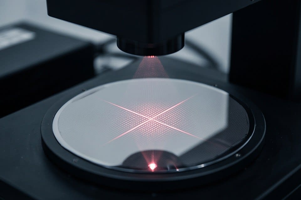
How Vision Inspection Algorithms Work
In semiconductor processes, visual inspection or simple sensor based methods struggle to reliably detect surface defects at the level of a few micrometers. Vision inspection algorithms combine machine learning and digital image processing to analyze wafer or package surfaces as high resolution images and automatically classify defect locations and types.
Deep learning based models use electron microscope images as input and learn through a generative adversarial neural network structure. As repeated training accumulates, detection boundaries become more refined. It is also possible to trace back which process stage caused a specific defect pattern, making the technology useful for blocking defect causes early. Thanks to a parallel processing structure that handles dozens of defect candidates simultaneously in a single image, inspection speed can keep pace with process speed even on high speed production lines.
The criteria used by the algorithm are clear. How different is the target from the normal pattern, and does that difference exceed the process tolerance range. Ultimately, how well an algorithm is trained determines the upper limit of semiconductor yield.

Effects of an Integrated Cleaning and Inspection Process
When cleaning and inspection are operated as separate processes, residual contaminant particles left after cleaning may pass through the inspection stage and move on to later processes. In semiconductor cleaning, the micro nanobubble method disperses bubbles with diameters of 0.1μm or less in water to physically separate contaminant particles from the surface. In the case of a bubble array cleaning device using acoustic vibration, a maximum jet flow velocity of 148.5mm/s was achieved, and a cleaning efficiency of 92.5% has been reported.
Even when cleaning efficiency is high, if residual contamination is not immediately verified through inspection, it becomes difficult to identify the cause of yield variation during the process. Huvics provides a solution that combines its proprietary ultrasonic dispersion technology and vision inspection algorithm within a single process flow. A structure in which image based inspection follows immediately after cleaning quickly identifies the point where defects occur in product groups that are sensitive to microscopic contamination, such as MLCC multilayer ceramic capacitor and FPCB flexible printed circuit board processes.
The same approach is applied in ultra precision component manufacturing sites where contamination tolerance standards are extremely low, such as camera modules and autonomous driving sensors. Integrating cleaning and inspection to shorten the in process feedback loop is becoming an important direction in semiconductor manufacturing.
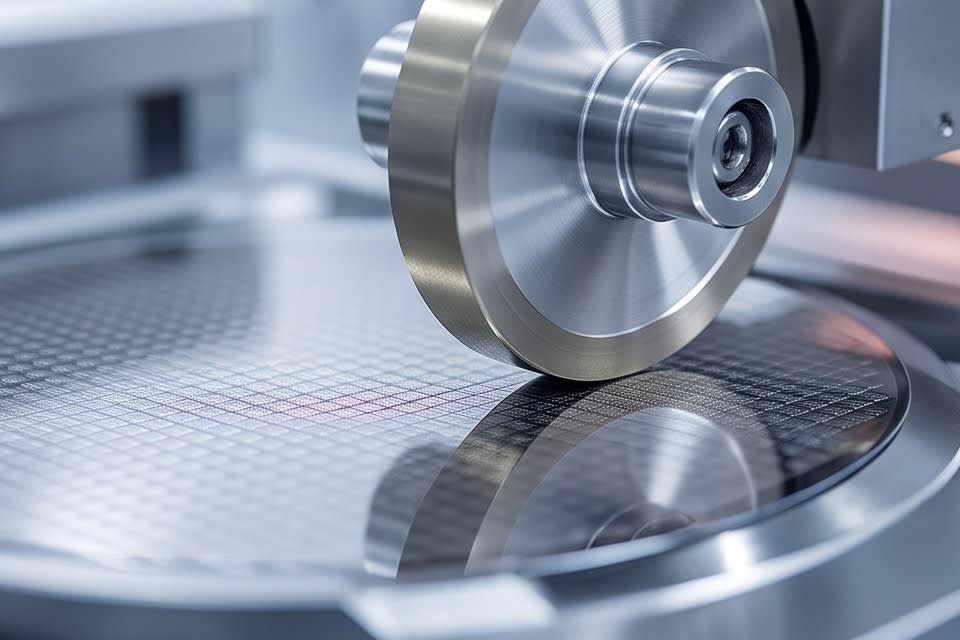
Linking Ultra Precision Grinding with Vision Inspection
As the markets for AI semiconductors and high performance memory semiconductors expand, package structures that vertically stack dozens of chips are rapidly increasing. In stacked structures, thickness errors in each layer accumulate, so maintaining thickness uniformity during the grinding stage determines the reliability of the final product.
Required Level of Thickness Uniformity
In 3D integrated circuit manufacturing, the thickness uniformity required for ultra thin grinding is a total thickness variation TTV of less than 0.5μm based on a 300mm wafer, which is a tolerance range narrower than one 150th of the diameter of a human hair. DRAM memory wafers are generally ground to about 50μm, while MEMS wafers are ground to about 30μm. Optimizing the contact angle between the grinding wheel and the wafer surface serves as a key factor in improving TTV.
Configuration and Application of the PKG Grinder
Huvics PKG Grinder uses a high precision stage and diamond wheel to achieve micron level precision machining, and supports various package types including FCBGA, WLCSP, QFN/DFN, and solar cells. It is available in Full Auto and Manual Type configurations, allowing flexible application according to the automation level of the production line while ensuring stable quality even in high speed processes.
When the post grinding flow is linked with a vision inspection algorithm that verifies thickness uniformity and surface condition, the precision of yield management across the entire process advances to the next level. This is where the significance of ultra precision grinding technology becomes clear as a process foundation that supports the performance and reliability of next generation semiconductor packages.

In semiconductor manufacturing, reducing the defect rate ultimately comes down to how quickly and accurately information within the process can be read. When these three processes are connected into one flow, with vision inspection algorithms finding defects in images, cleaning technology removing the causes of contamination, and ultra precision grinding controlling thickness errors within the tolerance range, yield can finally reach a stable trajectory. Even if one stage performs exceptionally well, if the others cannot keep up, the causes of defects will continue to appear elsewhere. A viewpoint that designs the entire process in an integrated way is the starting point of semiconductor quality management.
Huvics is an advanced technology company that develops and manufactures automation equipment and
production systems across the semiconductor, LED, Mobile, and Cosmetic industries.
With top talent and continuous technological innovation, we support improved customer productivity and
help secure quality competitiveness.
Huvics Contact Information
Tel: 031-374-8285
Email: cdpark@huvics.com
