Tag: YieldImprovement

  • A Field Case That Made the Difference Between 95% and 75% Yield, How Are You Designing Your Cleaning Process?

    A Field Case That Made the Difference Between 95% and 75% Yield, How Are You Designing Your Cleaning Process?

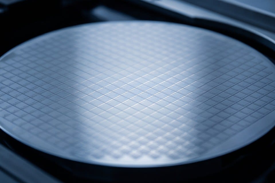
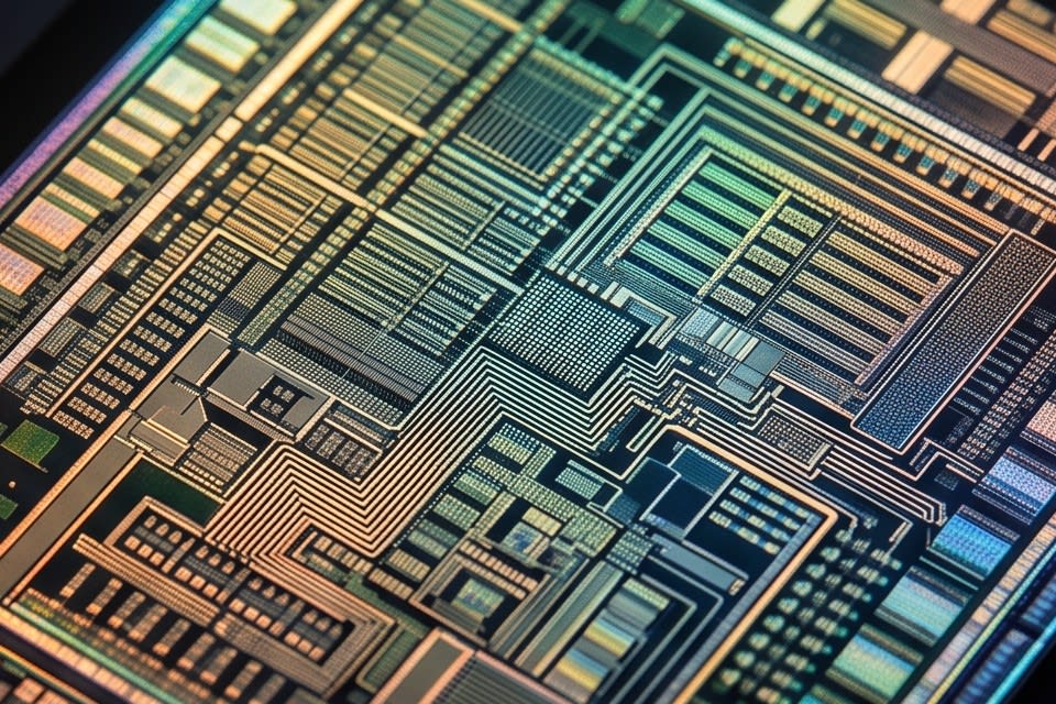
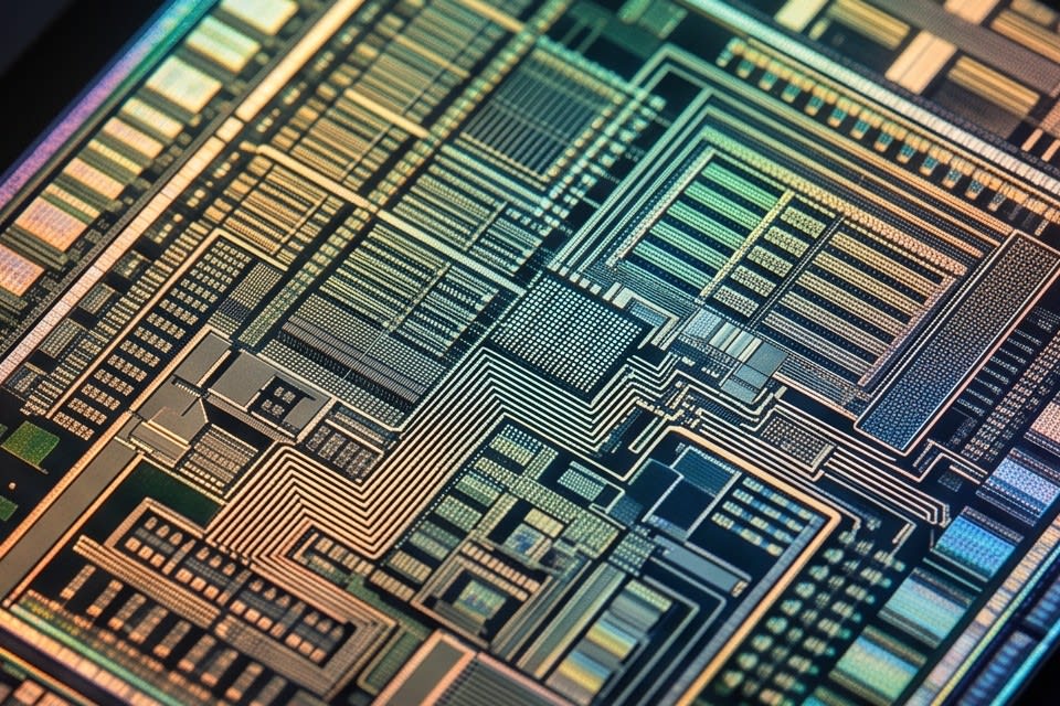
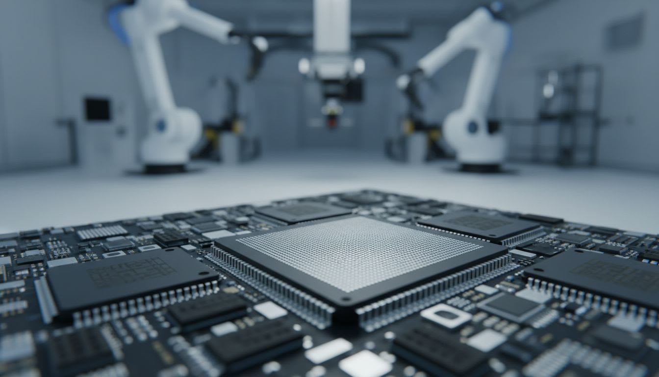
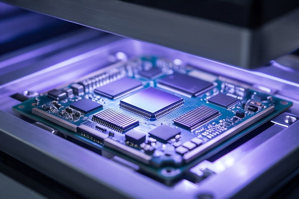
    Fine die structures on the surface of a wafer, a key material in semiconductor manufacturing

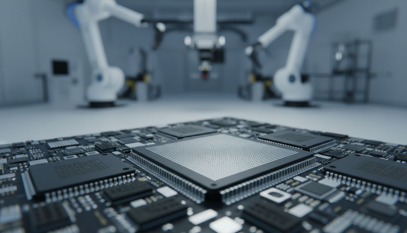
    In semiconductor manufacturing sites, some view the cleaning process as the ‘finishing stage’. However, the fact that a single contaminant particle can change the fate of an entire wafer shows that cleaning is not the end of the process, but a variable that determines yield.

    The Impact of a Single Contaminant Particle on Yield

    In semiconductor manufacturing, contaminant particles reduce yield in ways that cannot be seen with the naked eye. If a single submicron particle lands on a wafer during the photolithography process, the entire die can become unusable. According to Applied Physics USA, this is a real cause that separates a 95% yield from a 75% yield.

    As processes move down to 3 nanometers and 2 nanometers, the allowable contamination level becomes even narrower. A single contaminant particle can lead to the disposal of an entire wafer, and the resulting loss can reach millions of dollars. As processes become finer, the role of cleaning is elevated from simply maintaining cleanliness to serving as a line of defense for yield.

    No matter how well a cleanroom environment is prepared, particles generated during the process are targets for control, not something that can be considered completely eliminated. Ultimately, a clear trend has taken hold in semiconductor manufacturing sites, where final quality stability is determined by how cleaning equipment removes particles and at which stage it does so.

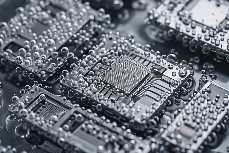
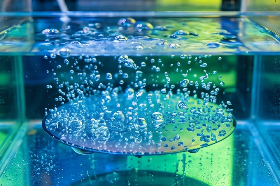
    Micro bubble cleaning method in which fine bubbles cover the surface of a semiconductor chip

    Structure and Role of Multi Step Cleaning Technology

    To effectively remove contaminant particles, a single cleaning method has limitations. This is because the nature of contamination varies, including particles loosely attached to the surface, foreign matter embedded in fine grooves, and residual liquids generated during the process. To address this, multi step cleaning methods are being adopted in the field.

    • Micro Bubble is a method in which fine bubbles contact the surface and separate particles without physical impact, making it suitable for removing contamination while minimizing surface damage to precision components.
    • Water Jet directly removes surface contamination using a high pressure water stream.
    • Air Knife blows away residual moisture after cleaning and prevents contamination from reattaching before the drying stage.
    • When the Oven Dry function is added, the process flow from cleaning to drying is completed as one integrated sequence.

    Huvics Cleaner System is designed so that this multi step configuration can be applied according to the characteristics of products such as camera modules, sensors, VCM motors, and trays, and it can be selected as either Full Auto or Manual depending on site conditions. When selecting cleaning equipment, the key is not a single performance figure, but a step configuration suited to the contamination type and product shape.

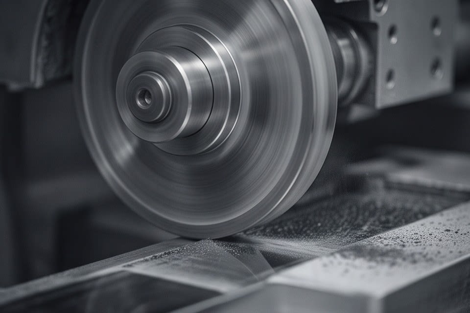
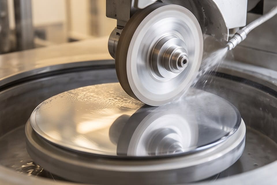
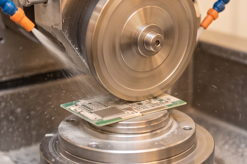
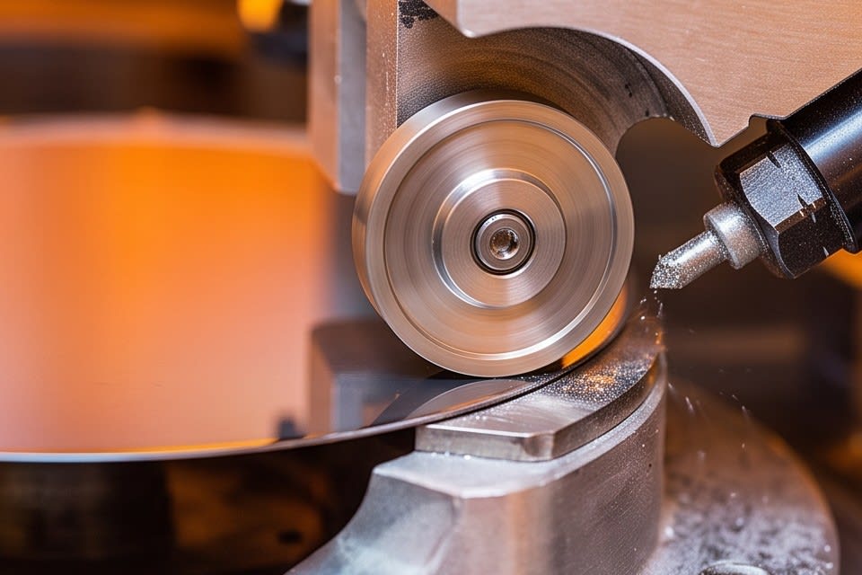
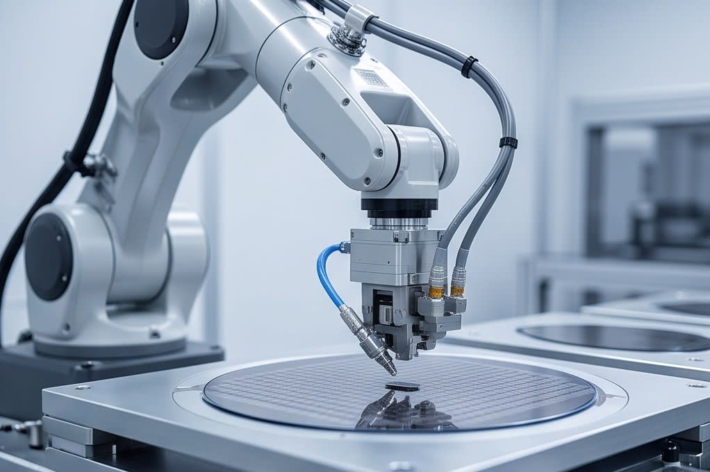
    A high speed rotating diamond wheel processing a semiconductor package at the micron level

    The Link Between Machining Precision and Cleaning Efficiency

    Engineers responsible for chip stacking processes know very well how sensitive package thickness variation can be as a variable. In structures where dozens of chips are stacked vertically, such as AI semiconductors or high performance memory, the thickness uniformity and flatness of each layer are directly connected to signal transmission and bonding reliability. When thickness variation accumulates, it can lead to poor electrical connections or heat dissipation issues, which is like planting the seeds of yield loss even before the cleaning stage.

    Huvics PKG Grinder uses a high precision Stage and Diamond Wheel to achieve micron level thickness uniformity. It supports a wide range of package types, including FCBGA, WLCSP, QFN/DFN, and Solar Cell, and can reliably process products to the thickness targets required by customers. It supports both Full Auto and Manual modes, ensuring flexibility in production line configuration.

    By minimizing quality variation even in high speed processes, it creates the conditions needed to maximize the effectiveness of the subsequent cleaning process. Machining precision determines cleaning efficiency, and cleaning efficiency determines final yield. The significance of the PKG Grinder is confirmed by the fact that these two processes are connected.

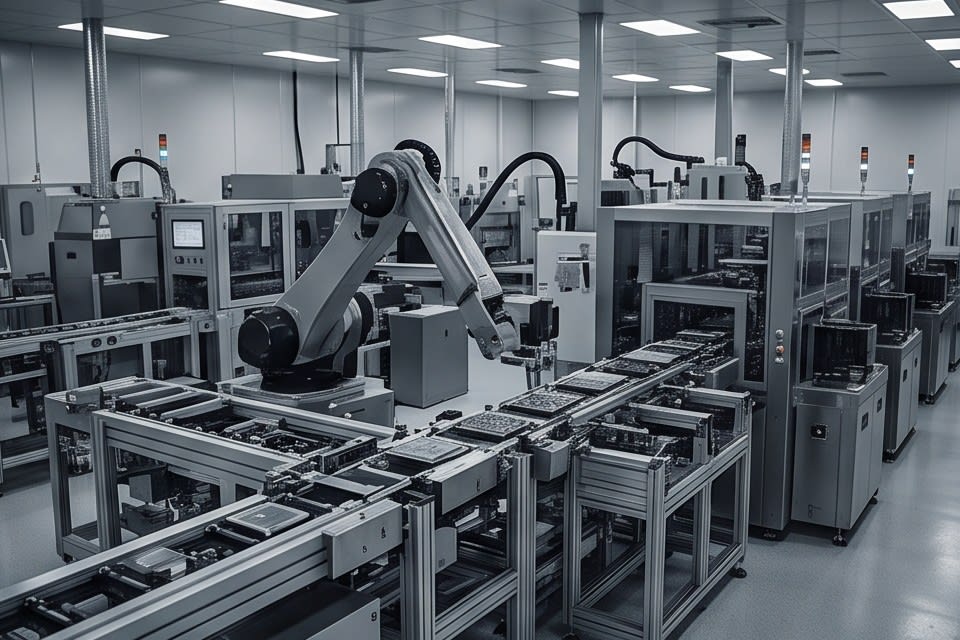
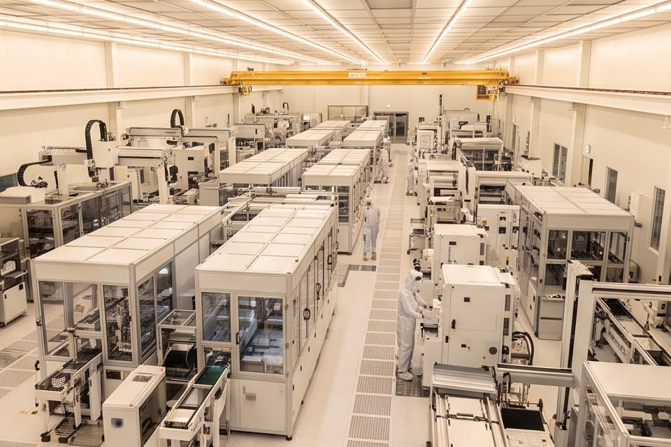
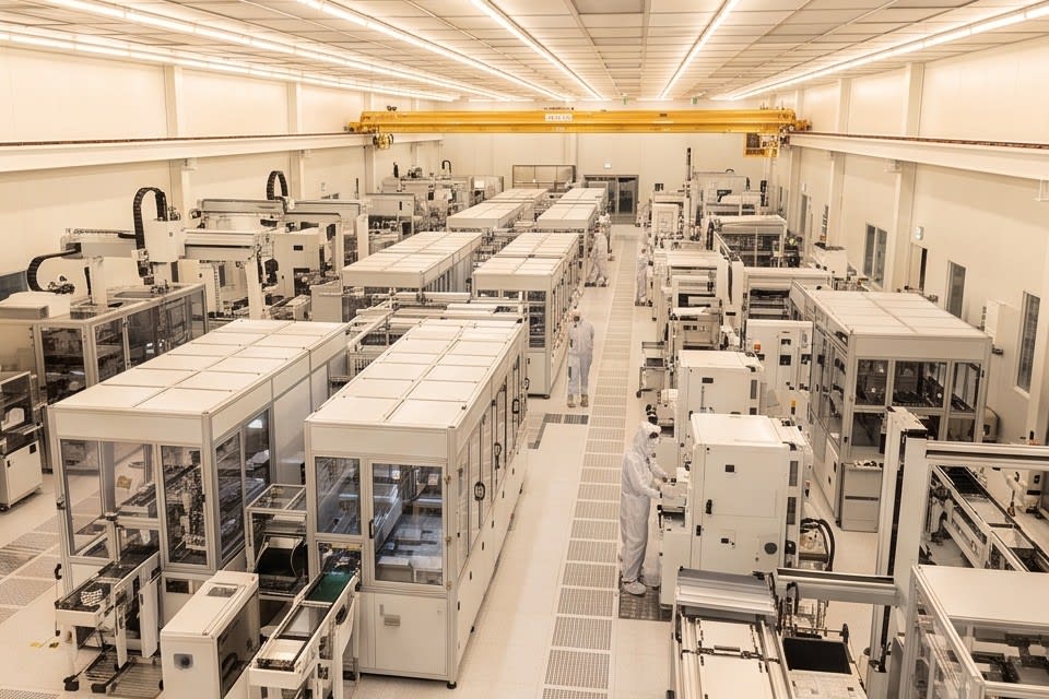
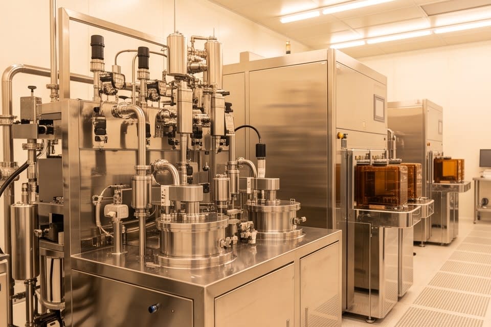
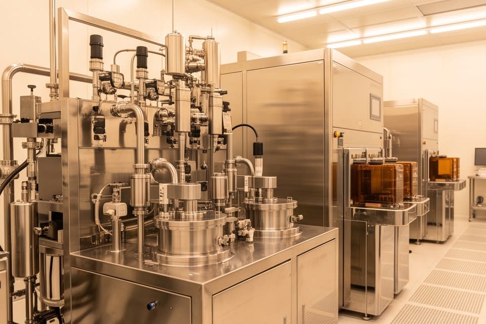
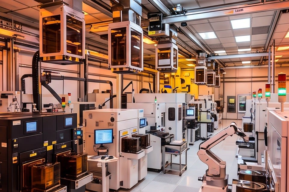
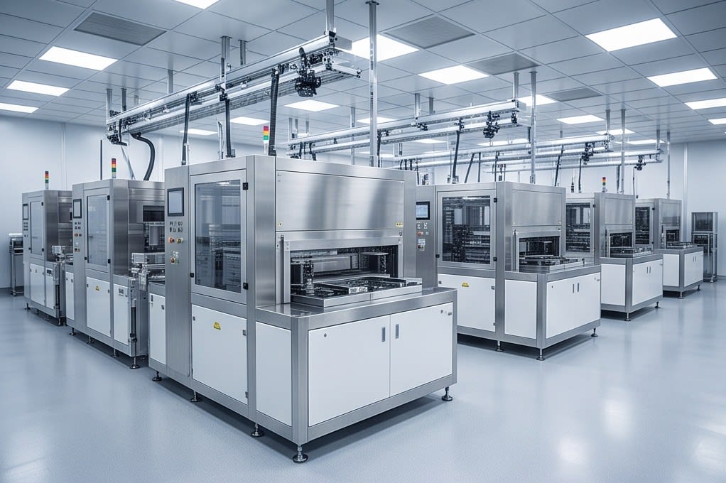
    Interior of a cleanroom with a multi step cleaning system and automated process line installed

    When choosing cleaning equipment, many people commonly focus only on cleaning power. However, because the type of contamination, the shape of the product, and the requirements of the subsequent process all differ, the criteria for equipment selection must also change. Understanding the structure in which machining precision supports cleaning efficiency and the cleaning method determines final yield is the starting point for semiconductor process design.


    Huvics is an advanced technology company that develops and manufactures automation equipment and
    production systems across the semiconductor, LED, Mobile, and Cosmetic industries.
    With top talent and continuous technological innovation, we support customers in improving productivity and
    securing quality competitiveness.

    Huvics Contact

    Tel: 031-374-8285
    Email: cdpark@huvics.com

    Huvics Inquiry

  • AI Semiconductor Packaging Yield: How to Improve It Step by Step from Grinding to Cleaning

    AI Semiconductor Packaging Yield: How to Improve It Step by Step from Grinding to Cleaning

    A semiconductor packaging process site where multiple pieces of equipment are organically connected

    When I first looked closely at a semiconductor packaging site, there was one question customers commonly asked. “The grinding went well, so why do defects keep appearing during bonding?” That question once again confirmed that the root of the problem is not a single piece of equipment, but the entire flow of the process. At that site, I learned firsthand that even a slight deviation in flatness can affect every layer built on top of it.

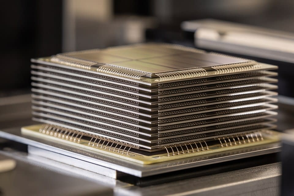
    A semiconductor stacked structure with dozens of dies precisely stacked vertically

    Why flatness is critical in AI semiconductor packaging

    HBM(High Bandwidth Memory), now a core component of artificial intelligence semiconductors, is built by vertically stacking dozens of thin dies. In a 12 layer stack, each die is about 50 micrometers thick, but when the stack increases to 16 layers, the die must be thinned to about 30 micrometers. As the die becomes thinner, the rigidity of the wafer itself decreases, and the risk of warpage and cracking during the process increases as well.

    Variation in surface flatness is not simply a dimensional issue. According to a technical report from Applied Materials, even minute surface variations directly affect bonding quality and yield. As the number of stacked layers increases, the requirements for thickness uniformity in each layer become stricter, and tolerances become narrower. As package types such as FCBGA, WLCSP, and QFN become more diverse, these requirements become even more complex. Ultimately, flatness control in the packaging process is not optional. It is a variable that determines yield itself.

    A process scene in which a wafer surface is finely ground using a diamond wheel

    How the grinding process determines flatness

    The grinding process is a key step that determines the thickness and surface flatness of semiconductor dies. Unlike general cutting processes, precision grinding uses a diamond wheel to remove material in micron units while achieving the desired thickness and flatness at the same time. The tolerance achievable through precision grinding is around ±0.001~0.005mm, and surface roughness reaches Ra 0.2~0.8μm. This is 5~10 times more precise than general CNC milling.

    These figures matter not simply because they show how precise the process is, but because that precision directly determines the bonding quality of the subsequent bonding process. Grinding equipment that combines a high precision stage with a diamond wheel must be able to maintain thickness uniformity even in high speed processing. It is also important to have a configuration that allows flexible selection between fully automatic and manual types depending on the nature of the production line. Huvics PKG Grinder is designed to uniformly process various package types such as FCBGA, WLCSP, and QFN down to the thickness required by the customer. Choosing a grinding machine also means deciding the precision level for the entire process.

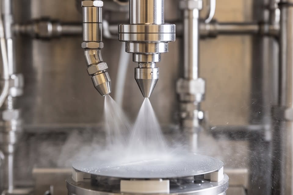
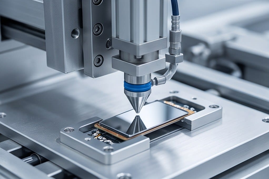
    A process of washing the die surface immediately after grinding by spraying cleaning liquid through a precision nozzle

    Why cleaning after grinding must be treated as one integrated step

    The die surface after grinding is in its most vulnerable state during the process. If fine particles and residues generated during grinding remain on the surface, they can lead to bonding defects in subsequent bonding or packaging steps.

    According to technical data from MSP/TSI, particle removal efficiency in the cleaning process is determined by multiple factors such as cleaning time, temperature, chemical concentration, and agitation method. How precisely these variables are controlled determines final quality. Simply rinsing with water makes it difficult to effectively remove residual particles at the submicron level.

    Huvics cleaning system uses a multi stage method that combines micro bubbles, water jets, and an air knife to remove surface contamination particles step by step, and its oven drying function handles residual moisture after cleaning. When analyzing the process of a customer who came with a camera module defect rate issue, repeated residual particles were occurring because the agitation conditions in the cleaning step had not been optimized. In semiconductor tray cleaning as well, the key was to design different cleaning conditions according to complex contamination types. This is exactly why how a surface precisely processed by grinding is finished in the cleaning step can completely change the value of the process.

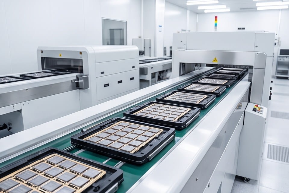
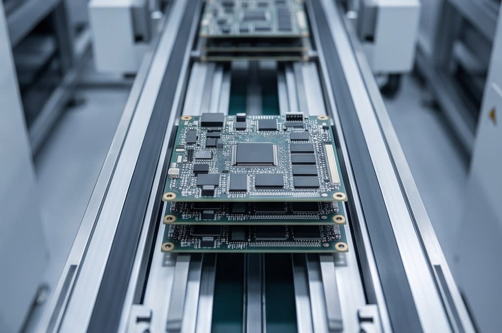
    Automated semiconductor process equipment organically connected along a conveyor belt

    The precision of the stacked structure required by AI semiconductors cannot be completed by the performance of grinding equipment alone. Only when cleaning can fully preserve the flatness created by grinding do those numbers truly have meaning. The two processes must be designed as one continuous flow. That is the real standard that determines packaging quality.


    Huvics is an advanced technology company that develops and manufactures automation equipment and
    production systems across the semiconductor, LED, Mobile, and Cosmetic industries.
    With top talent and continuous technological innovation, we support customers in improving productivity and
    securing quality competitiveness.

    Huvics Contact

    Phone: 031-374-8285
    Email: cdpark@huvics.com

    Huvics Inquiry

  • From Semiconductor Cleaning to Grinding, Step-by-Step Process Technologies That Protect Yield

    From Semiconductor Cleaning to Grinding, Step-by-Step Process Technologies That Protect Yield

    Semiconductor cleaning equipment implementing a multi-stage cleaning combination

    In semiconductor processes, cleaning was long considered a finishing stage. It was widely viewed as a supporting procedure that removes foreign matter before moving on to the next process. However, as chip integration has increased and package structures have become more complex, we have entered an era where a single cleaning method can determine overall yield. What type of bubbles are used, in what sequence drying takes place, and at what pressure cleaning is performed are now treated as key variables in process design.

    A micro-nano bubble generation scene that removes contamination by distributing fine bubbles in water

    Two Requirements of Cleaning Technology: Removal and Preservation

    The core of cleaning technology lies in removing contaminant particles while fully preserving the product surface. These two requirements conflict with each other. Increasing cleaning power raises the risk of surface damage, while choosing a safer method can leave residual contamination behind.

    The micro jet method instantaneously generates energy reaching thousands of atmospheres and thousands of degrees, and for fine pattern structures below 70 nanometers, this energy itself can become a source of damage. For this reason, in cleaning equipment design, energy control and dispersion methods become key criteria that define the level of technology.

    The micro-nano bubble method distributes bubbles with a diameter of 0.1 micrometers or less in water to separate surface contamination, an approach designed to secure cleaning performance without physical impact. Multi-stage cleaning design combines different principles in this way to respond to the types of contamination generated at each process step.

    For products with complex surface structures and sensitive internal components, such as camera modules, sensors, and VCM motors, the limitations of a single cleaning method are clear. Combining Micro Bubble, Water Jet, and Air Knife step by step, while controlling residual moisture through Oven Dry functionality, is a configuration designed to meet these complex requirements. In processes where cleaning quality is directly linked to the final defect rate, which technology combination to choose is no longer a matter of equipment specifications, but a matter of process strategy.

    A micron-level precision grinding process in which a rotating diamond wheel uniformly processes the substrate surface

    Package Thickness Uniformity and Ultra-Precision Grinding Technology

    Another variable that determines the quality of semiconductor processes as much as cleaning technology is the uniformity of package thickness. In structures where multiple chips are vertically stacked, such as AI semiconductors and high-performance memory, thickness variation in each layer affects both electrical characteristics and mechanical reliability. It is also known that in RF applications, substrate thickness and resistivity affect parasitic capacitance, thereby determining signal integrity.

    The semiconductor industry roadmap requires wafer bonding processes to achieve thickness uniformity within ±5% across the entire wafer surface. If this standard is not met, stacking itself becomes meaningless.

    Huvics PKG Grinder performs micron-level grinding for various package types such as FCBGA, WLCSP, and QFN/DFN by using a high-precision stage and diamond wheel. It is available in Full Auto and Manual Type configurations to secure production line flexibility while being designed to maintain consistent thickness uniformity in high-speed processes. Regardless of which package structure is selected, how tightly thickness variation is managed is the key factor that separates product grade and yield.

    An operator wearing a cleanroom suit manually inspecting a wafer through a microscope

    The Impact of Automation Transition on Yield and Availability

    As the precision of process technology increases, the importance of how equipment is operated to implement it consistently also grows. Processes manually performed by skilled operators rely on individual experience and judgment, which creates structural limitations in repeatability and reproducibility. Even with the same equipment, results vary depending on the operating method, and those differences lead to yield variation in mass-production environments.

    Cases have been reported in which efficiency increased by approximately 17.6% when a systematic yield improvement framework was introduced compared with manual empirical methods. Automation transition is not simply a matter of increasing speed, but of securing process consistency and predictability. According to a McKinsey report, improving equipment reliability can increase tool availability in fabs by more than 15%. Higher availability means fewer unplanned equipment stops and maintenance gaps, which connects directly to the stability of the overall production plan.

    A configuration that combines Full Auto and Manual options is a strategy for flexibly responding to these needs, and many cases have accumulated in manufacturing sites where the level of process automation has been increased step by step.

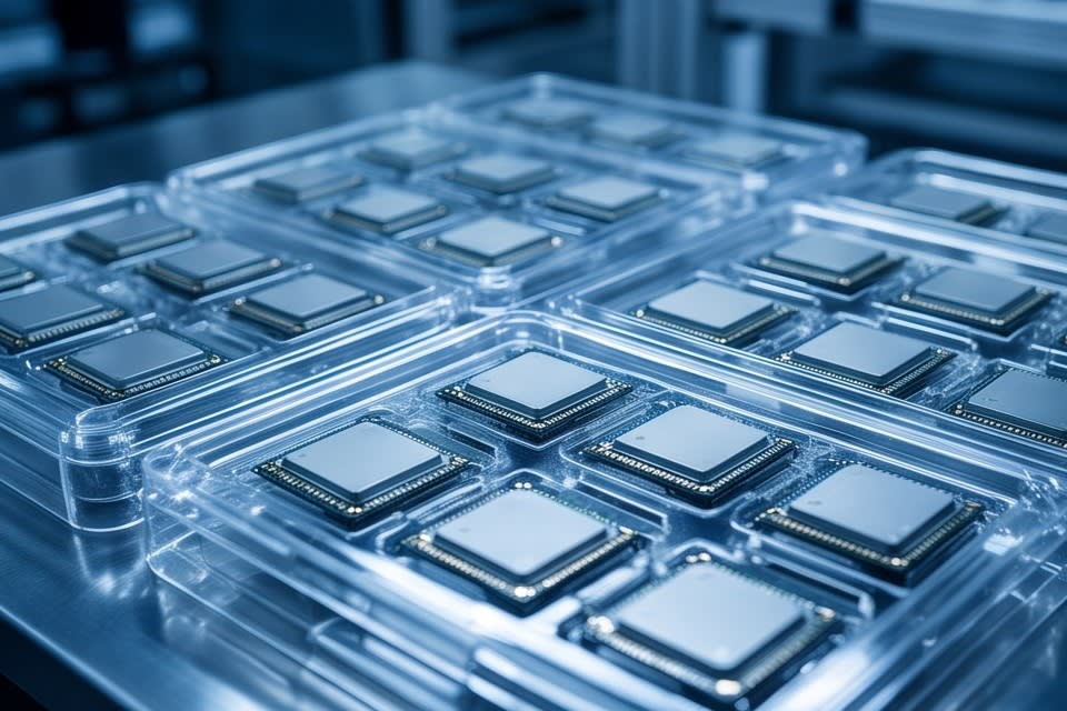
    Semiconductor chips arranged in a tray after securing quality through cleaning and grinding

    In semiconductor processes, cleaning and grinding may appear to be separate technical domains, but they ultimately converge on the same question. How should the surface be handled so that the next process can proceed reliably. Bubble size, pressure control, thickness uniformity, equipment availability, all these variables make up the details of the process, and the sum of those details determines the reliability of the final product. Yield is not reserved at the design stage, but is protected or lost at every step of the process.


    Huvics is an advanced technology company that develops and manufactures automation equipment and
    production systems across the semiconductor, LED, Mobile, and Cosmetic industries.
    With top talent and continuous technological innovation, we support customers in improving productivity and
    securing quality competitiveness.

    Huvics Contact Information

    Phone: 031-374-8285
    Email: cdpark@huvics.com

    Huvics Inquiry

  • Why Process Integration Determines Yield in Semiconductor Cleaning, Grinding, and Lamination

    Why Process Integration Determines Yield in Semiconductor Cleaning, Grinding, and Lamination

    Finely designed semiconductor circuit patterns

    According to data from Semiconductor Equipment and Materials International (SEMI), a significant share of defects in semiconductor processes is reported to originate from particle contamination. This means that a single particle just a few micrometers in size, invisible to the naked eye, can undermine the yield of an entire chip. As processes become more miniaturized and package structures grow more complex, the precision of each stage, including cleaning, drying, grinding, and lamination, is emerging as a key factor that determines final product quality. By examining which technologies control these variables, we can see the direction in which digital transformation in semiconductor manufacturing is moving.

    Bubbles generated in liquid surrounding a semiconductor substrate

    Structure and Principles of a Multi-Stage Cleaning and Drying System

    Contaminants remaining on semiconductor surfaces are especially difficult to handle because they are not visible. Fine contamination made up of organic matter, metal residues, and particles is difficult to remove through simple physical washing. The approach developed to solve this problem is multi-stage cleaning technology.

    According to a study published in the Korean Journal of Chemical Engineering, a cleaning system using acoustic bubble arrays was shown to remove fine particles of various wettability and sizes with an efficiency of 92.5%. Microbubbles are generated at sizes of 5 nm or less, physically and chemically separating oils and fine particles from the substrate surface, while the following water jet pushes away suspended contaminants. In the air knife stage, remaining moisture and particles on the surface are removed by airflow, and the final oven drying process completely evaporates any moisture left after cleaning.

    Huvics’ 4-stage cleaning and drying system is designed to process this sequence within a single line. For automotive electronics components such as camera modules or autonomous driving sensors, which require both optical cleanliness and electrical reliability, a structure that continuously controls the process through drying is especially important. This is because residual moisture can lead to poor adhesion or corrosion in subsequent processes. The industry is shifting from a method that separated cleaning and drying into individual processes toward an integrated inline system.

    Processing the surface of a semiconductor wafer with a metal wheel and rotating tool

    Grinding and Lamination That Improve Package Process Precision

    As demand for AI semiconductors and high-performance memory increases, package structures are becoming increasingly complex. This is because the mainstream is shifting away from enclosing a single chip in encapsulant and toward structures that vertically stack multiple chips. This change is fundamentally raising the requirements for the grinding process.

    Thickness Uniformity in the Grinding Process

    In stacked packages, even a thickness deviation of only a few micrometers in each layer can directly lead to electrical connection defects or heat dissipation issues. According to published data from the patent office, rough grinding in the package grinding process takes about 2.5 to 5 minutes, while finish grinding takes about 2 to 4 minutes. The key is achieving the target thickness uniformly within this short time. Because required thickness and surface roughness differ by package type, such as FCBGA, WLCSP, and QFN/DFN, equipment must be able to combine diamond wheels with high-precision stages and set conditions differently at the micron level.

    Integrated Structure of the Lamination Process

    The same applies to the lamination process. If equipment is changed at each stage from tape mounting to UV curing, alignment errors accumulate between processes. To reduce this, a one-stop structure that processes everything from the expander to UV curing within a single system is being introduced. How well the processes can be integrated and how precisely the conditions of each stage can be controlled is the key factor that determines next-generation package yield.

    Overview of a manufacturing site with automated equipment arranged in a row

    Cleaning, grinding, and lamination may appear to be independent processes, but these three stages are connected as one quality chain. If the surface is not completely cleaned, grinding precision becomes unstable, and if thickness after grinding is not uniform, lamination adhesion becomes uneven. Digital transformation in semiconductor manufacturing is not an abstract concept. It begins with precisely controlling each of these connected links through data and automation.


    Huvics is an advanced technology company that develops and manufactures automation equipment and
    production systems across the semiconductor, LED, Mobile, and Cosmetic industries.
    With top talent and continuous technological innovation, we support customers in improving productivity and
    securing quality competitiveness.

    Huvics Contact

    Tel: 031-374-8285
    Email: cdpark@huvics.com

    Huvics Inquiry

  • A Guide to Innovating Mobile Component Manufacturing Processes with the Huvics One Stop Laminator System

    A Guide to Innovating Mobile Component Manufacturing Processes with the Huvics One Stop Laminator System

    Huvics

    Consumer expectations for thinner and more powerful mobile devices continue to rise, but behind the scenes, the challenges on the manufacturing floor are becoming even more complex. At a time when even a nearly invisible microscopic contaminant can disrupt product yield, protecting flawless quality within complex processes has become a core priority for manufacturers.

    If you are weighing efficiency against precision due to waiting times and unexpected variables that arise while moving between equipment, now is the time for an innovative shift that changes the standard of productivity. Through the one stop laminator system proposed by Huvics, let us explore a new standard for next generation semiconductor manufacturing processes that goes beyond complexity.

    Ultra precision mobile component process

    Precision Process Innovation in Mobile Component Manufacturing

    Today, mobile devices are becoming slimmer and more powerful with each passing day. At the center of this change is a precision process in which microscopic components, almost invisible to the naked eye, are organically integrated. Especially in semiconductor and advanced component manufacturing sites, even one tiny contaminant can sharply reduce product yield, making perfect precision cleaning more than just one part of the process. It has become an essential survival strategy that determines the completeness of the product.

    Manufacturers must now move beyond simple cleaning steps and consider how to optimize efficient laminating and curing processes in stacked packaging.

    Features of the One Stop Laminator System

    In response to these industry needs, Huvics proposes an innovative one stop laminator system that integrates tape mounting and ultraviolet curing technology into one solution. The key features of this system are as follows.

    • Organically processes everything from expansion to ultraviolet curing within a single process
    • Significantly shortens tact time by simplifying complex manufacturing processes
    • Secures process stability and fundamentally blocks factors that cause quality defects

    Integrated ultraviolet curing line

    Maximizing Production Efficiency Through Process Integration

    The true value of the one stop laminator system proposed by Huvics lies in its seamless integration of previously complex and interconnected manufacturing processes into a single structured system. In conventional manufacturing sites, waiting time during transfer was unavoidable because products had to pass through multiple pieces of equipment in sequence.

    However, the Huvics system is designed so that every step from the expander to the final ultraviolet curing stage is performed continuously on a single line, fundamentally eliminating these bottlenecks. The benefits provided by this unified process structure are as follows.

    Key Benefits of a Unified Process

    • Minimizes numerous variables that may occur in the manufacturing environment
    • Maintains consistent and stable quality even in mass production systems
    • Fundamentally blocks external contamination factors that may occur during transfer between equipment

    Smart factory view

    Ultraviolet Curing Technology and Quality Reliability

    The ultraviolet curing stage that follows the cleaning process is a critical turning point that determines the durability of components and the completeness of packaging. The Huvics system applies precise ultraviolet curing technology at this key stage to maximize bonding strength and secure the structural stability of the entire packaging process.

    In particular, the finely controlled curing system optimizes the properties of the adhesive, effectively preventing component warping or delamination that may occur during assembly. The significance of this advanced control capability is as follows.

    Value of Advanced Control Capability

    • Completes product reliability by physically blocking factors that cause quality defects
    • Provides a foundation for taking the precision of mobile component manufacturing to the next level
    • Serves as a smart investment to ensure the highest level of defect free product quality

    Stacked packaging process

    Ultraviolet curing process

    Automated process

    Ultimately, the core of manufacturing competitiveness lies in removing process complexity and fully controlling even the smallest variables that may affect quality. The Huvics one stop laminator system achieves both production speed and precision, presenting the production standard that next generation semiconductor manufacturing sites should pursue.

    To ensure that your valuable technology is not diluted under the name of process, experience higher yield and overwhelming quality completeness through the most reliable and smart integrated solution available today.


    Huvics is an advanced technology company that develops and manufactures automation equipment and
    production systems across the semiconductor, LED, Mobile, and Cosmetic industries.
    With top talent and continuous technological innovation, it supports the improvement of customer productivity and
    the securing of quality competitiveness.

    Huvics Contact

    Phone: 031-374-8285
    Email: cdpark@huvics.com

    Huvics Inquiry

  • Huvics 4-Stage Cleaning and Drying System-Next-Generation Solution for Quality Innovation in Ultra-Precision Components

    Huvics 4-Stage Cleaning and Drying System-Next-Generation Solution for Quality Innovation in Ultra-Precision Components

    Huvics

    In manufacturing sites that handle ultra-precision components such as semiconductors and autonomous driving sensors, invisible microscopic contaminants are the greatest challenge directly linked to critical defects. No matter how advanced the technology integrated into a product may be, even a single particle of fine dust or residual moisture left behind during the cleaning process can severely disrupt the yield of the entire production line.

    Is your current process fully controlling these invisible threats? In an era where manufacturing competitiveness is difficult to discuss without a systematic system that goes beyond simple cleaning and fundamentally blocks the possibility of defects, let us take a closer look at a solution that minimizes complex process steps while securing stability that easily exceeds the strict quality standards required by the automotive electronics industry.

    Contaminant Removal Challenges in Ultra-Precision Industries

    In advanced component manufacturing sites such as semiconductors, the most critical and difficult challenge is to completely remove invisible microscopic contaminants and secure process yield. In ultra-precision industries where a single speck of fine dust can determine the quality of an entire product, incomplete contaminant removal directly leads to lower productivity and cost losses.

    Huvics 4-Stage Cleaning and Drying System

    Huvics has deeply analyzed these concerns in manufacturing sites and built the following 4-stage cleaning and drying system.

    • Precision cleaning through microbubble technology
    • Contaminant removal using a water jet
    • Moisture control using an air knife
    • Final drying through oven drying

    This next-generation solution, created based on proprietary process analysis, effectively controls contaminants hidden within the complex surface structures of ultra-precision components such as camera modules and autonomous driving sensors. Its batch-processing approach, which not only cleans but also completely removes residual moisture, meets the strict quality standards of the automotive electronics industry and maximizes operational stability at manufacturing sites.

    Through innovative cleaning processes, Huvics goes beyond simply reducing defect rates and works as a partner that fundamentally enhances the manufacturing competitiveness of customers.

    Huvics integrated cleaning solution

    Efficiency and Completeness of the Integrated Process

    The greatest competitiveness of the Huvics solution lies in its ability to handle every process from cleaning to drying seamlessly within a single system. It fundamentally blocks the possibility of external contamination that can occur when components move through multiple process steps on site.

    For ultra-precision components such as camera modules and autonomous driving sensors, even the smallest amount of residual moisture can cause critical quality damage such as circuit corrosion or functional degradation, making process completeness more important than anything else. The advanced oven-drying function built into the Huvics system was designed precisely to solve these on-site challenges.

    This function immediately optimizes the condition of components by thoroughly removing residual moisture right after cleaning. As a result, manufacturing sites can maintain a perfect quality level without any separate additional drying process or complicated transfer procedure.

    As a result, Huvics minimizes unnecessary process steps while realizing value beyond the strict standards expected by customers through its unmatched technology of zero residual moisture.

    Smart factory automated process

    Quality Standards and Technological Innovation in the Automotive Electronics Industry

    As the automotive electronics industry advances rapidly today, the quality standards required for components have become stricter than ever before. The production of components that cannot tolerate even the smallest defect, such as sensors for autonomous vehicles or semiconductor chips, has now entered an area that cannot be solved by relying solely on equipment performance.

    Amid these changes, the competitiveness of manufacturing sites ultimately depends on what level of technology is used to secure process stability and control even the smallest variables. Huvics deeply understands these industrial demands and focuses on maximizing operational stability in production lines through precision cleaning technology.

    Beyond simply supplying cleaning equipment, we continue to prove our value as a key partner in next-generation manufacturing processes that ensure reliability across the entire manufacturing process. To ensure that technological innovation leads directly to real benefits on production sites, Huvics will continue to support customers in achieving a higher level of quality innovation through precise and robust solutions.

    Perfectly dried components

    Strategic Asset for the Future Manufacturing Environment

    The future of advanced industries will ultimately be determined by how precisely and efficiently processes can be controlled. The 4-stage cleaning and drying system proposed by Huvics is becoming a strategic asset that changes the manufacturing paradigm, going beyond the simple adoption of equipment.

    While many companies are engaged in a difficult battle against defect rates, Huvics provides proactive responsiveness that removes even invisible threats through innovative process analysis. Through our integrated solution, customers experience improved productivity by achieving higher quality results with fewer resources.

    If you are considering precise control and a batch-processing system in line with the changing industrial environment, Huvics will be the most reliable answer. Based on continuous technology development and field-centered thinking, Huvics will continue to fulfill its role as a dependable technology partner leading quality innovation in the global automotive components industry beyond Korea.

    Batch processing drying system

    A Partner for Quality Innovation

    In ultra-precision industries where a single invisible microscopic contaminant can determine a company’s success or failure, precision has now become an essential strategy for survival beyond a simple virtue. Through the 4-stage integrated cleaning and drying system built on innovative process analysis, Huvics solves the complex challenges faced by manufacturing sites in the most efficient and complete way.

    The technology of Huvics, which expands the limits of quality and strengthens process reliability, will become a dependable partner that brings new competitiveness to your production site. If you are considering quality innovation, now is the time to begin a higher leap toward a next-generation manufacturing environment with Huvics.

    Efficient production line


    Huvics is an advanced technology company that develops and manufactures automation equipment and
    production systems across the semiconductor, LED, Mobile, and Cosmetic industries.
    With top talent and continuous technological innovation, we support customers in improving productivity and
    securing quality competitiveness.

    Huvics Contact

    Phone: 031-374-8285
    Email: cdpark@huvics.com

    Huvics inquiry

  • Laminator Performance That Determines Semiconductor Yield and Huvics’ Process Optimization Strategy

    Laminator Performance That Determines Semiconductor Yield and Huvics’ Process Optimization Strategy

    Huvics

    As semiconductor microfabrication reaches its limits, even a 1% yield difference in the final stage of the production line has emerged as a key variable that determines corporate profitability. However, many manufacturing sites still rely on standardized laminator operation methods, often failing to control minute errors caused by changing environments and wasting valuable resources.

    Are the pressure and temperature control methods in your current process truly ready to break through their limits? Recognized for its technological capability in the global market by receiving the USD 1 Million Export Tower on Trade Day 2025, Huvics proposes a process optimization solution that goes beyond simple equipment adoption and presents a new standard for production efficiency.

    Advanced laminating equipment by Huvics

    The Importance of the Laminator Process and the Role of Huvics

    As semiconductor manufacturing processes become increasingly miniaturized, the importance of laminators that determine bonding quality on wafer surfaces is greater than ever. While laminating was once considered a secondary step that simply attached materials, in today’s semiconductor ecosystem, the laminator has become a critical variable that determines the yield of the entire production line depending on the uniformity of equipment pressure and the precision of temperature control.

    Technical Foundation for Precision Processes

    In an advanced manufacturing environment where even the smallest error cannot be tolerated, minimizing defects in the laminating process is a mission-critical issue directly tied to corporate profitability. Huvics deeply understands these technical challenges in manufacturing sites and has built its own technical foundation through years of research and development to maximize the precision of laminating processes.

    Beyond being a simple equipment supplier, we prove our value as a strategic partner that solves customers’ manufacturing challenges based on the following strengths.

    • Possession of 2 proprietary patented technologies
    • Extensive field project experience
    • Precise technical support solutions

    Inside a precision laminator chamber

    Process Optimization Realized Through Customized Solutions

    The 2 patented technologies held by Huvics fundamentally resolve the process challenges that inevitably occur during laminator operation and are optimized to maintain uniform quality in any environment. Because many manufacturing sites rely only on standardized equipment, they often suffer yield declines when unable to respond to irregular environmental changes that occur in actual production fields.

    Field-Centered Customized Strategy

    Huvics moves beyond this inertia by closely analyzing each customer’s unique manufacturing environment and designing customized total solutions that maximize production efficiency. This process helps prevent bottlenecks that frequently occur in the field and dramatically improves the efficiency of equipment operation.

    Above all, the close technical support system of Huvics becomes a reliable foundation for securing stable yield even within complex and precise manufacturing processes. This is the core driving force that leads customers beyond short-term improvement toward achieving the strategic goal of long-term process optimization. Through Huvics solutions that combine technical expertise with field-centered thinking, your processes will gain a level of sophistication and strong competitiveness unlike before.

    Advanced engineering expertise

    Technical Credibility Recognized by the Global Market

    The technical credibility of Huvics, proven by receiving the USD 1 Million Export Tower in the global market, demonstrates that we are the most reliable partner in the ever-changing semiconductor manufacturing field. We do not remain merely as a supplier of hardware. In the face of rapidly changing technical challenges, we provide systematic analysis based on process data and a continuous feedback loop.

    Know-How for Maximizing Production Yield

    To increase production yield, more than simply introducing equipment is required. Operational know-how that can maximize the equipment’s potential is essential. This is exactly where the Huvics approach begins. We provide practical momentum that helps customers break through the limits of production yield and maintain stable quality.

    Huvics solutions, which advance laminator performance beyond its technical limits, ultimately strengthen customers’ market competitiveness and deliver essential value in completing the final quality of semiconductor products. Today, when precise process control directly leads to corporate profitability, Huvics proposes the success formula most optimized for your production site.

    Automated laminating process

    Sustainable Semiconductor Process Innovation

    In the semiconductor industry, process optimization is not a static goal but a process that must continuously evolve. Whenever wafer size and circuit line width change, the physical limits of pressure and temperature control that the laminator must handle also change. Huvics reads these waves of change ahead of time and proactively solves the technical challenges customers will face tomorrow.

    Integrated Value Creation and Future Vision

    Our process optimization strategy goes beyond simple technical support. By comprehensively identifying the issues faced by customers’ production sites, it creates integrated value that extends the overall lifespan of equipment and reduces operating costs. Many sites that have introduced Huvics solutions have achieved not only yield improvement but also the additional benefit of enhanced operator understanding of the process.

    This clearly shows that technology does not remain merely a tool, but plays a central role in innovating a company’s production culture. Huvics will stand with you to the end as a reliable technical partner on your journey to establish a new standard for semiconductor production efficiency. Realizing the infinite potential of your processes with the highest quality and optimal efficiency is the true value pursued by Huvics.

    Large-scale production line of Huvics

    As proven by the USD 1 Million Export Tower award on Trade Day 2025, the technological capability of Huvics goes beyond simply supplying equipment and is redefining the standard for global semiconductor production sites. In an era when even minute errors in the laminating process directly lead to yield risks, what your company must choose is not the equipment itself, but a precise control solution capable of breaking through the limits of production efficiency.

    Huvics’ customized strategy, designed based on 2 proprietary patents and extensive field know-how, will become the most reliable driving force for your processes to maintain peak performance and secure sustainable competitiveness. For your site as it begins change today, the technical expertise of Huvics will serve as a reliable partner and complete a new success formula.


    Huvics is an advanced technology company that develops and manufactures automation equipment and
    production systems across the Semiconductor, LED, Mobile, and Cosmetic industries.
    With top-tier talent and continuous technological innovation, we support customers in improving productivity and
    securing quality competitiveness.

    Huvics Contact Information

    Phone: 031-374-8285
    Email: cdpark@huvics.com

    Contact Huvics

  • 3 Core Technologies of the Huvics One Stop Laminator System That Improve Semiconductor Process Efficiency

    3 Core Technologies of the Huvics One Stop Laminator System That Improve Semiconductor Process Efficiency

    Huvics

    A semiconductor manufacturing site is an intensely competitive battlefield where every minute and every second of efficiency becomes technological competitiveness. In a semiconductor line where countless micro processes operate in close coordination, improving process efficiency is a core indicator that determines a company’s competitiveness.

    Until now, many production sites have handled the essential processes of tape mounting and ultraviolet curing independently using separate equipment. However, this separated operation method has created invisible barriers, including lead time caused by movement between facilities and the inconvenience of management.

    Huvics One Stop Laminator System

    Innovation of the One Stop Laminator System

    Huvics presents an innovative solution called the One Stop Laminator System to address these structural challenges in semiconductor manufacturing processes. By integrating previously separated process steps into one, it boldly removes the physical gaps that had hindered manufacturing efficiency. The key features of this system are as follows.

    • Supports both lamp type and LED type ultraviolet curing systems
    • Offers precision control capabilities optimized for the characteristics of each film
    • Prevents damage to heat-sensitive components through process simplification

    One Stop Process Flow Diagram

    Extreme Precision Control Technology

    The point where Huvics technology stands out most in the field lies in its precision control capability that maintains extreme levels of detail. The various adhesive films used in semiconductor back-end processes require different curing conditions depending on the type.

    The Huvics system is designed to finely adjust the optimal irradiation intensity for each difficult-to-handle film. In a semiconductor environment where even the smallest variable cannot be tolerated, this precision control system becomes an essential element for ensuring stable quality.

    Precision Ultraviolet Curing Module

    Maximizing Process Stability and Production Yield

    Electronic components that are especially sensitive to heat can be at risk of physical deformation from even slight temperature changes. Through its distinctive cooling and output control technologies, Huvics fundamentally prevents substrate damage and maximizes process stability. This meticulous process management delivers the following results.

    • Improves process efficiency beyond simply reducing defect rates
    • Provides customers with a higher level of production yield
    • Becomes the foundation for building a stable process environment

    Smart Control Panel

    The power to break down the complex barriers of semiconductor manufacturing comes from the simplicity of removing unnecessary steps and the precision that fills the process. The Huvics One Stop Laminator System is a technological achievement completed after relentless efforts to pursue efficiency, promising customers flawless process stability and dramatic yield improvement.

    When it is time to secure both production speed and product value, the technological completeness of Huvics will provide the most reliable support for your site.


    Huvics is an advanced technology company that develops and manufactures automation equipment and
    production systems across the semiconductor, LED, Mobile, and Cosmetic industries.
    With top-tier talent and continuous technological innovation, we support customers in improving productivity and
    securing quality competitiveness.

    Huvics Contact Information

    Phone: 031-374-8285
    Email: cdpark@huvics.com

    Huvics Inquiry

  • A Complete 4-Step Checklist for Selecting Semiconductor Cleaning Equipment from Start to Finish

    A Complete 4-Step Checklist for Selecting Semiconductor Cleaning Equipment from Start to Finish

    Huvics

    The Starting Point of Semiconductor Process Innovation, a New Standard for Selecting Cleaning Equipment

    Just a few years ago, when introducing semiconductor cleaning equipment, it was considered natural to compare only the visible, impressive specifications of the equipment or the figures listed in specification sheets. However, as manufacturing processes have recently become extremely miniaturized, it has become more important than ever to precisely diagnose the actual conditions of our production line and verify the corresponding, unrivaled ultra-precision control technology step by step. For companies seeking to achieve perfect yield and secure sustainable technological competitiveness, a systematic cleaning equipment selection checklist will become the most essential milestone that determines successful process innovation.

    Step 1: Precise Analysis of Our Process Conditions and Contamination Sources

    The Importance of Understanding Actual Process Conditions

    Among the many stages of semiconductor manufacturing, cleaning is undoubtedly the key factor that determines perfect yield. Therefore, the journey toward introducing the ideal semiconductor cleaning equipment must begin with the first step of examining the actual conditions of our process as closely as if through a microscope. Many field managers often make the mistake of first reviewing the impressive equipment specifications or specification sheets available on the market when introducing new equipment. However, no matter how expensive or high-performing the equipment may be, it is of no use if it does not match the physical and chemical characteristics of the cleaning targets handled on our line.

    Contamination Source Analysis and Cleaning Mechanism

    Therefore, before comparing equipment, the following preliminary analyses must be carried out first.

    • Analyze the fine dimensions of the wafers to be processed
    • Identify the detailed materials of the substrates used in the process
    • Determine the exact types of fine contaminants to be removed

    The reason this preliminary analysis is important is that the appropriate cleaning mechanism varies completely depending on the type of contaminant, such as whether it must be physically removed or dissolved through a chemical reaction. For example, organic contaminants and inorganic contaminants require completely different removal methods, and the pressure applied or fluid flow must also be precisely controlled depending on the shape of the fine patterns formed on the wafer surface. Securing reliable quantitative preliminary data that clearly identifies the composition of contamination sources is the strongest first step in preventing unexpected equipment introduction failures or process errors.

    Step 2: Detailed Review of Spatial Limitations and Target Production Volume

    Analysis of Spatial Factors in the Production Line

    At the same time, it is essential to carefully examine the spatial limitations that the actual production line can accommodate and the target production volume that must be achieved each day.

    Before introducing equipment, rough guidelines should be established by considering all of the following spatial factors.

    • Check efficient movement routes inside the cleanroom
    • Inspect utility connection conditions for equipment operation
    • Secure the minimum workspace required for maintenance

    Professional cleanroom semiconductor cleaning equipment line

    Huvics, which has earned strong trust in global advanced industries through its ultra-precision cleaning and automation equipment technologies, also provides reliable guidance based on extensive experience and unrivaled ultra-precision technology so that customers can prepare this first step as thoroughly as possible. After such a thorough and precise preliminary diagnosis process, you will gain sharp insight that allows you to clearly define the optimal equipment specifications truly required for your process.

    Automated Transfer Systems and Maximized Efficiency

    Wafer batch processing that ensures consistent quality

    In particular, automated transfer systems help optimize logistics routes and fundamentally prevent operator-induced contamination. Automation solutions that maximize production line efficiency are a core element in preventing process errors and maintaining consistent quality. Through this, improved yield and stable line operation can be achieved at the same time.

    Automated wafer transfer process using a robot arm

    Step 3: Verification of Ultra-Precision Control Technology and Global Reliability

    The Need for Ultra-Precision Control Technology

    Once the actual conditions of our process have been precisely analyzed and objective baseline data has been successfully secured, it is time to move on to the next step, selecting the optimal cleaning method and verifying the core technological capabilities of the equipment. As semiconductor processes have recently become extremely miniaturized to the level of tens of thousands of times thinner than a strand of hair, the presence of ultra-precision control technology capable of completely removing fine contaminants without causing even 1 nanometer of damage to the substrate has become the decisive standard that determines the success or failure of equipment selection. If equipment without sufficient technological capability is introduced, contaminants may be removed, but the delicately formed fine circuit patterns may collapse or become damaged, ultimately leading to the painful result of mass defects.

    Technology and Reliability Verified in the Global Market

    Therefore, when objectively comparing candidate equipment, it is essential to thoroughly verify through a checklist whether the equipment has the precision processing capability and pressure control capability to penetrate between extremely fine patterns and completely wash away contaminants. At this point, the safest and most reliable selection criterion is to choose a specialized manufacturer that has already been recognized in the global market for outstanding technology and unrivaled reliability as a partner. This is precisely why Huvics, which has continuously delivered exceptional results and led process innovation in advanced technology fields requiring high precision, including not only semiconductors but also LED and mobile industries, is attracting attention as a representative choice.

    In particular, based on uncompromising and outstanding technological potential, Huvics received the 1 Million Dollar Export Tower award on Trade Day in 2025, proudly earning recognition for its technological value and reliability not only domestically but also in the global market. By carefully comparing and reviewing the core source technologies of manufacturers verified by credible institutions and markets, as well as their actual delivery records to major corporations and global processes, you will gain the outstanding insight needed to objectively and sharply select the optimal equipment that most perfectly fits your production line among numerous equipment candidates without hesitation.

    Ultra-precision cleaning liquid spray through a precision nozzle

    Step 4: Maintenance and After-Sales Support Capabilities for Long-Term Productivity

    Maintenance for Long-Term Performance Retention

    If you have carefully verified the specifications and core technological capabilities of the equipment suited to your process through the previous steps, it is now time to face the final step, which is both the most important and the one that determines long-term productivity, evaluating the ease of maintenance after equipment introduction and the continuous technical support capabilities of the supplier. Since semiconductor cleaning equipment is highly precise equipment that must continuously control extremely fine contamination at the nanometer level, it is most important to maintain the initial performance at the time of first installation and operation consistently for many years without any change. This is because, no matter how excellent the equipment may be, if even a slight error or component wear occurs during operation and cannot be addressed quickly, the entire production line may come to a halt, resulting in astronomical losses.

    Checklist Criteria and After-Sales Support Infrastructure

    To thoroughly prevent this, the following items must be set and evaluated as key checklist criteria.

    • Periodic calibration support for precise sensors and control devices
    • Fast and stable supply system for consumables and replacement parts
    • After-sales management infrastructure capable of immediate response when issues occur

    From this perspective, Huvics, which has built long-standing trust by always serving as a dependable and reliable partner in the successful business journeys of numerous global leading companies, goes beyond the role of a simple equipment supplier and demonstrates exceptional after-sales technical support capabilities as a true process partner that works together to ensure the long-term stabilization of customers’ processes. A systematic after-sales management system plays a decisive role in extending equipment lifespan and minimizing unexpected downtime. Through this, companies can maintain stable productivity over the long term.

    Robust precision hardware components of cleaning equipment

    The Optimal Partnership for Successful Process Innovation

    Only when you finally choose a partner that clearly guarantees continuous management and partnership after introduction can you reliably secure consistent process stability and firmly build sustainable future technological competitiveness in the rapidly changing global semiconductor market. As a result, by thoroughly completing this final step, readers will go far beyond a temporary and short-term equipment purchase and successfully introduce a perfect cleaning solution that maximizes the operating rate and production efficiency of the entire manufacturing line, along with a trustworthy partner for the long term.

    A wafer shining in gold after cleaning is complete

    Until recently, selecting cleaning equipment based only on impressive equipment specifications was considered natural, but today, when ultrafine processes lead the industry, a step-by-step checklist covering everything from preliminary diagnosis to after-sales maintenance has become the absolute standard for successful equipment introduction. Only by going through a systematic process that begins with precise data analysis suited to your process, verifies core technological capabilities, and confirms long-term partnership can you finally complete a perfect cleaning solution that maximizes line operating rates. Begin this reliable journey with Huvics, which has proudly proven its unrivaled ultra-precision technology and reliability in the global market, and firmly build sustainable future technological competitiveness in the rapidly changing semiconductor market.


    Huvics is an advanced technology company that develops and manufactures automation equipment and
    production systems across the semiconductor, LED, Mobile, and Cosmetic industries.
    With top talent and continuous technological innovation, we support customers in improving productivity and
    securing quality competitiveness.

    Huvics Co., Ltd. Contact

    Phone: 031-374-8285
    Email: cdpark@huvics.com

    Contact Huvics

  • Why Semiconductor Cleaning Processes Matter and Everything About Huvics’ 4-Stage Cleaning Technology

    Why Semiconductor Cleaning Processes Matter and Everything About Huvics’ 4-Stage Cleaning Technology

    Huvics

    The Dilemma of Ultrafine Semiconductor Processes and a New Cleaning Paradigm

    Until now, semiconductor manufacturing sites have mainly relied on simple cleaning methods that use strong physical pressure spraying or high-concentration chemical detergents to remove invisible microscopic contaminants. However, in today’s ultrafine processes, where circuit spacing has become extremely narrow at the level of just a few nanometers, these harsh methods can instead cause critical damage by creating tiny scratches on sensitive substrate surfaces or collapsing structures. Yet if the stimulation applied to the substrate is reduced indiscriminately, microscopic nanoparticles firmly attached to the surface cannot be removed properly, ultimately leading to massive wafer disposal. What is now needed is a completely new level of process approach, such as Huvics’ innovative precision cleaning technology, that can fundamentally block physical stress on materials while achieving complete contaminant control.

    Semiconductor wafer with future technology

    Microscopic Contaminants, the Unwanted Guests of Advanced Industries, and Their Critical Impact

    In today’s cutting-edge semiconductor, display, and core information technology industries, where countries around the world compete with national stakes on the line, the most critical unwanted guests are extremely fine contaminants that cannot be detected by the human eye. As devices become highly miniaturized and circuit spacing narrows to the nanometer level, microscopic contaminants have the following critical effects in today’s ultrafine manufacturing processes.

    • Causing circuit malfunction by obstructing current flow and triggering short circuits
    • Generating economic losses through the disposal of entire high-value semiconductor wafers

    In this way, even a single invisible particle can cause enormous disruption to the entire process.

    Precise wafer circuit pattern

    The Key to Determining Initial Yield, Huvics’ Precision Cleaning System

    For this reason, in semiconductor and advanced manufacturing processes, the cleaning process that secures initial yield by completely removing harmful particles that enter between process steps is considered a key factor that determines the final competitiveness of a product, just as much as assembly and packaging. In response to the demands of such highly sensitive and demanding industrial sites, Huvics has built unmatched technical precision and trust in the field of precision cleaning processes. Huvics’ precision cleaning system goes beyond the basic step of mechanically wiping foreign matter from component surfaces and is designed based on a thoroughly planned systematic guide to maximize the cleanliness of product surfaces. This advanced system performs the following roles.

    • Completely controls contamination variables at manufacturing sites
    • Reduces production costs and strengthens corporate competitiveness

    Through this, Huvics plays a leading role in improving customer productivity.

    Automated spray cleaning process

    Differentiation of the Proprietary 4-Stage Cleaning and Drying Guideline

    Limitations of Conventional Cleaning Methods and Technical Challenges

    The true differentiator of Huvics’ precision cleaning system is fully embodied in its proprietary 4-stage cleaning and drying guideline. The surfaces of precision semiconductor substrates or ultrafine sensor components have extremely sensitive and delicate physical structures, so if conventional cleaning methods such as high-pressure physical spraying or harsh high-concentration chemical detergents are applied as they are, critical damage such as micro scratches on the surface structure or structural collapse can easily occur. However, if the stimulation is reduced too much, fine nanoparticles firmly attached to the surface cannot be completely removed, creating a dilemma that leads to defects.

    Huvics’ Proprietary 4-Stage Cleaning and Drying Process

    To fully solve these technical challenges, Huvics divided the cleaning and drying process into four independent yet organically connected precision stages. In each area of the cleaning stage, variables such as surface tension, fine bubble size, chemical behavior, and cleaning solution temperature are applied in a customized way according to the characteristics of each component, safely separating and collecting only the dust attached to the surface without applying any microscopic physical stress to the material itself. Furthermore, in the drying process, where technical completeness is considered just as important as contaminant removal, secondary contamination caused by stains or residue from rapid temperature changes or moisture imbalance on the substrate surface is completely prevented. This thorough 4-stage flow, which allows no defects on component surfaces after drying, dramatically lowers process defect rates and serves as a key foundation that helps customers easily pass strict reliability tests.

    Delicate cleaning solution spraying process

    Maximizing Production Efficiency and Securing Competitiveness in the Global Market

    Introducing Huvics’ innovative precision cleaning solution into a production line brings groundbreaking results that go beyond a one-dimensional improvement of a single process and dramatically enhance the overall production efficiency of the entire factory. When precision in the cleaning stage is secured, the following direct economic benefits can be obtained.

    • Prevents process shutdowns and bottlenecks caused by microscopic contamination
    • Prevents raw material waste and shortens production cycles to maximize operating rates

    In particular, the ability to maintain uniform, stable, and top-tier quality from the new product development stage to mass production becomes a decisive key that enables customers to secure powerful technical credibility in the rapidly changing global semiconductor market.

    Process control by a precise robotic arm

    A Technology Partner Leading Next-Generation Semiconductor Processes

    As next-generation semiconductor processes that demand increasing miniaturization and higher integration arrive, the value of ultra-precision clean control technology continues to rise, and Huvics’ unmatched cleaning system is firmly recognized as an essential solution that cannot be overlooked in high-value-added high-tech manufacturing. Ultimately, through endless challenges without settling for the present, Huvics is establishing a differentiated paradigm in cleaning technology and elevating manufacturing standards and quality grades across the world’s most advanced industries to a more refined and trustworthy level.

    View of a cleanroom on a large-scale mass production line

    The Clear Choice for Defect-Free Quality

    In the end, the first task that must be achieved to win the competition in ultrafine semiconductor miniaturization is clean control technology that perfectly controls even invisible dust particles. As many manufacturing companies struggle with defect rates and yield declines caused by microscopic contamination, the systematic 4-stage cleaning and drying system presented by Huvics becomes the clearest solution for achieving complete cleanliness without process damage. In today’s market, where subtle differences determine product perfection and corporate competitiveness, experience a higher level of production efficiency and defect-free quality with Huvics’ unmatched precision cleaning solution.


    Huvics is an advanced technology company that develops and manufactures automation equipment and
    production systems across the semiconductor, LED, mobile, and cosmetics industries.
    With top talent and continuous technological innovation, we support customers in improving productivity and
    securing quality competitiveness.

    Huvics Contact

    Phone: 031-374-8285
    Email: cdpark@huvics.com
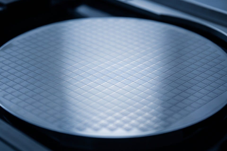
    Contact Huvics