Tag: chip stacking

  • When 1 Micron Determines Yield in the Field: Key Insights into the Chip Stacking Grinding Process

    When 1 Micron Determines Yield in the Field: Key Insights into the Chip Stacking Grinding Process

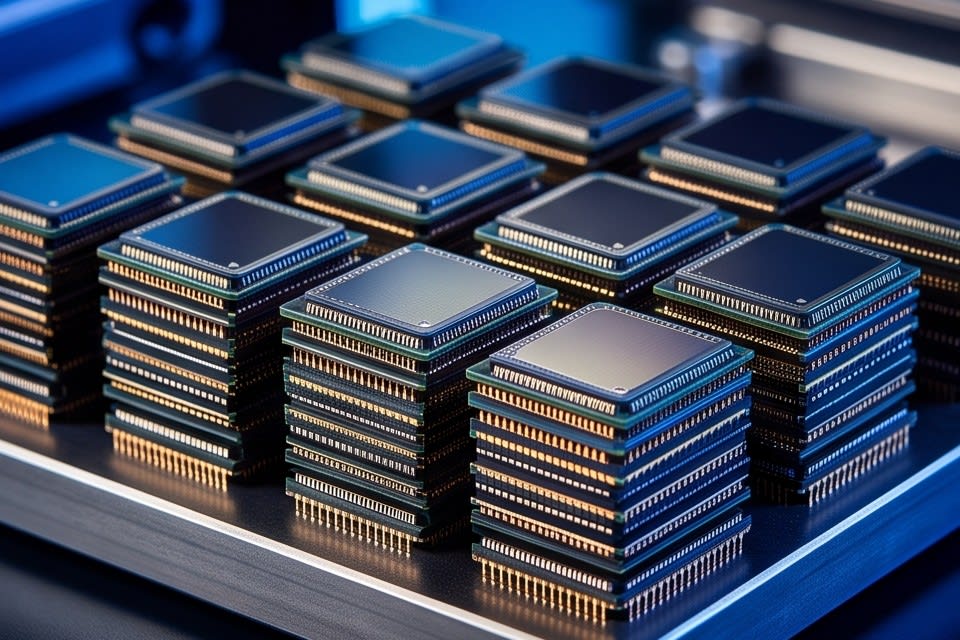
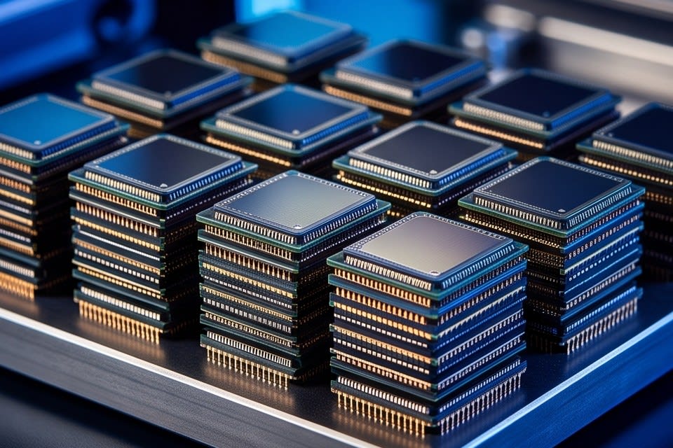
    Semiconductor chips neatly aligned and vertically stacked.

    There is a joke often shared among semiconductor design engineers. “The more chips you stack, the better, but the problem is that stacking them is far too difficult.” In real packaging processes where dozens of chip layers are stacked, the first thing to fail is not the design drawing, but flatness. In a world where a 1 micron difference can disrupt overall yield, the meaning of “grinding well” carries far more weight than expected.
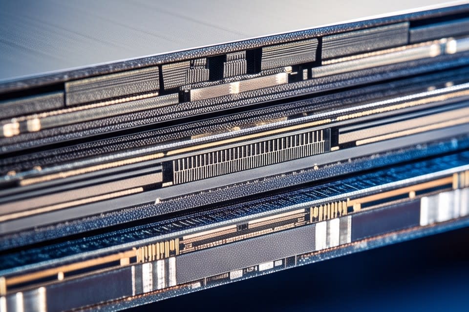
    A cross section of semiconductor chips precisely stacked with microscopic spacing.

    Why TTV Matters in Chip Stacking Structures

    In structures where chips are stacked in multiple layers, thickness variation in each layer is not just a dimensional issue. As layers accumulate, microscopic errors build up and eventually lead to electrical bonding defects or concentrated structural stress. The metric used to express this numerically is total thickness variation, or TTV.

    The TTV required in chip stacking structures is at the level of 1 micron or less, demanding precision far below one hundredth of the thickness of a human hair. If this standard is not met, bonding surfaces can lift during subsequent bonding processes or heat dissipation can become uneven, undermining the reliability of the device itself. For products such as AI semiconductors or high performance memory that vertically connect dozens of chips, the allowable variation range becomes even narrower.

    One reason TTV control is difficult in the field is the structural variables of the grinding equipment itself. The wear pattern of the grinding wheel, microscopic vibration generated during spindle rotation, and changes in the flatness of the chuck that fixes the wafer act together to make the thickness profile uneven. Uniform flatness cannot be achieved simply by turning on the equipment. How precisely these variables are controlled is the key factor that determines the yield of the entire packaging process.
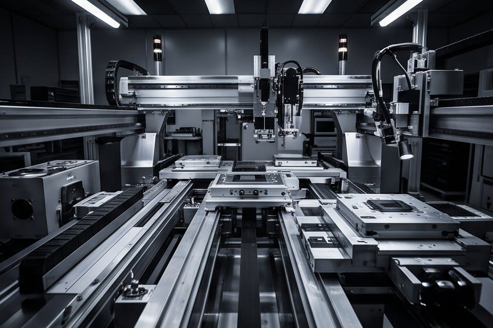
    Semiconductor process equipment equipped with a high precision stage and grinding head.

    Ultra Precision Grinding Design of the PKG Grinder

    There is a way to address this issue from the process equipment design stage. The PKG Grinder from Huvics combines a high precision stage with a diamond wheel to process various package types such as FCBGA, WLCSP, and QFN/DFN at micron level accuracy. The key is a control structure that keeps TTV variation within a defined range even during high speed processing. The TTV requirement for ultra thin wafer stacking processes is approximately 2.0 microns or less, and to meet this value reliably in a high speed grinding environment, spindle runout compensation and chuck flatness maintenance must be built into the equipment from the design stage.

    Another practical challenge in production sites is line flexibility. In many cases, the same equipment must handle both low volume high mix processes and high volume continuous production. The option to choose Full Auto A·B types or a Manual type is a design choice made to respond to this requirement, and it directly contributes to reducing setup loss during process changeovers. Speed and uniformity are usually in conflict, but in grinding equipment, they are implemented in a way that satisfies both conditions at the same time.
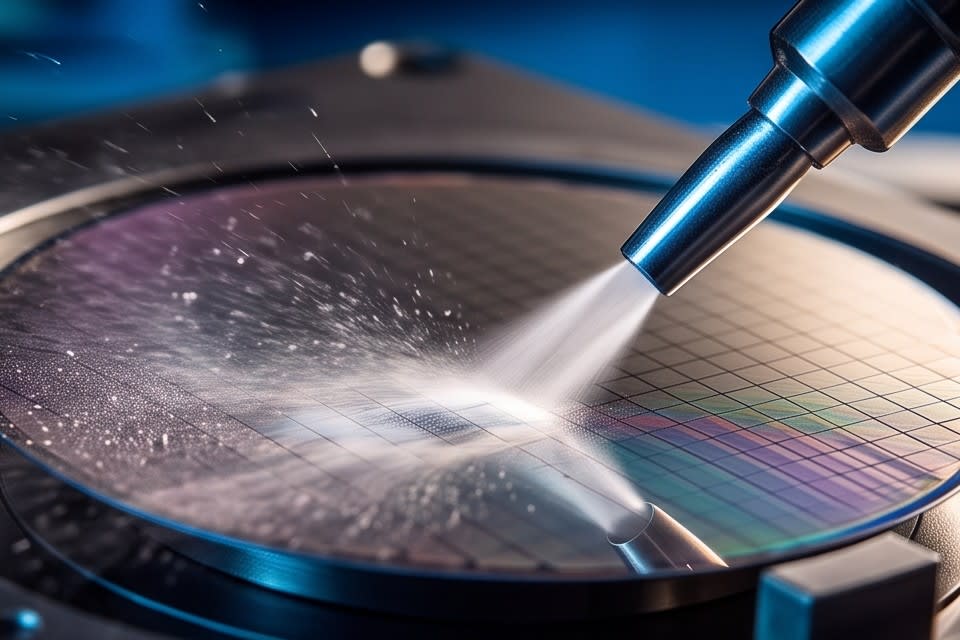
    Cleaning and drying process that removes surface residue after grinding.

    The Role of Cleaning and Drying After Grinding

    Flatness control does not end just because the grinding process is complete. Immediately after machining, grinding residue and fine particles remain on the wafer surface, and the way they are removed determines the final surface quality. This is where the choice of cleaning and drying methods becomes important.

    Comparison of Air Knife and IPA Vapor Drying

    The two drying methods mainly used in the industry are Air Knife and IPA vapor drying. Air Knife mechanically pushes liquid off the surface using a high speed gas jet, and according to research published on ResearchGate, drying within 2 seconds is possible under a speed condition of 150mm/s. In contrast, IPA vapor drying uses ultrapure isopropyl alcohol vapor to lower surface tension and guide moisture to flow away naturally without leaving marks.

    Because the two methods control processing speed and the risk of surface residue in different ways, the selection criteria vary depending on the surface characteristics of the target device and the process requirements.

    Multi Step Cleaning for Components Sensitive to Surface Contamination

    For components sensitive to surface contamination, such as camera modules, sensors, and VCM motors, a multi step cleaning approach that combines micro bubbles and water jets is becoming established.
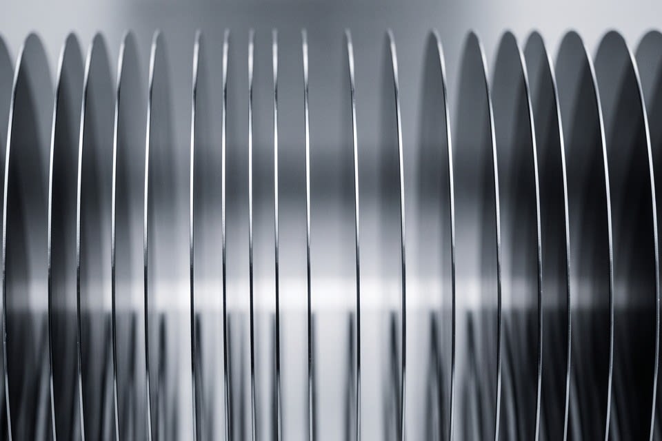
    A circular plate structure expressing the precision of the semiconductor chip stacking process.

    More than how many chips are stacked, how uniformly they are stacked determines the actual yield. From grinding precision to the selection of cleaning and drying methods, the quality of the packaging process is completed on a structure where each stage supports the next. The joke mentioned at the beginning, “stacking them is far too difficult,” turns out to describe the essence of process design quite accurately.


    Huvics is an advanced technology company that develops and manufactures automation equipment and
    production systems across the semiconductor, LED, Mobile, and Cosmetic industries.
    With top tier talent and continuous technological innovation, we support improvements in customer productivity and
    help secure quality competitiveness.

    Huvics Contact

    Phone: 031-374-8285
    Email: cdpark@huvics.com

    Contact Huvics

  • How to Manage Grinding, Lamination, and UV Curing Stages to Improve Chip Stacking Yield

    How to Manage Grinding, Lamination, and UV Curing Stages to Improve Chip Stacking Yield

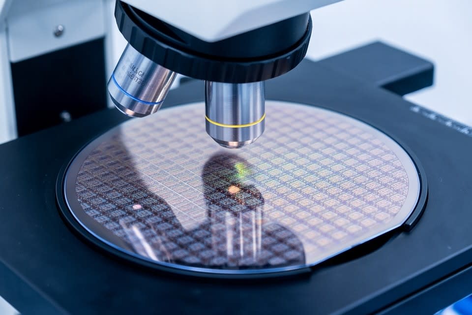
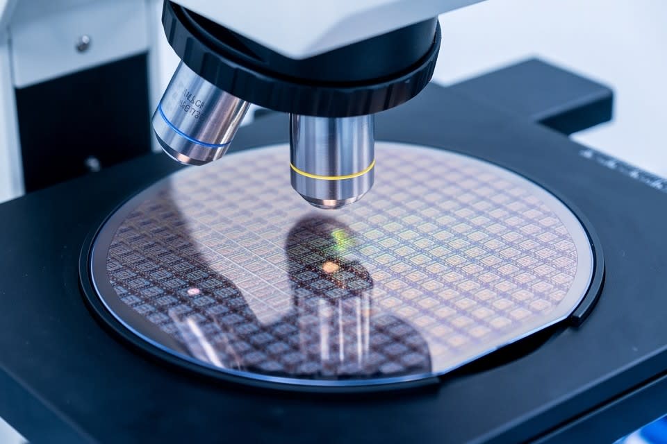
    A detailed inspection of a semiconductor wafer surface using optical equipment

    If you are an engineer designing semiconductor packages, you have probably encountered this situation at least once. Even after carefully setting the process conditions, step differences appear between chips after stacking, and yield data begins to fall below expectations. When tracing the root cause, the issue often comes down to thickness variation and flatness control. Even though this pain point is well known, the same trial and error is often repeated on production sites.

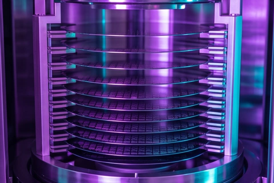
    Multiple wafers vertically aligned and stacked

    Why the shift to stacked structures made thickness control a prerequisite for the process

    As semiconductor package structures have shifted from single layer designs to stacked architectures, the thickness and flatness of each individual chip now require a level of precision that cannot be compared with the past. In single layer structures, a certain degree of thickness variation in individual chips could be tolerated, but in 3D stacked structures where multiple chips are stacked vertically, errors in each layer accumulate, meaning even one uneven chip can compromise the reliability of the entire package.

    In fact, research published on NCBI/PMC confirms that in advanced 3D stacking processes, chip thickness is reduced from around 780μm to 10μm or less, while total thickness variation TTV must be controlled to 1μm or below. As chips become thinner, the signal travel distance decreases, improving power efficiency, while lower thermal resistance also enhances heat dissipation performance.

    In this way, thinning is directly linked to performance improvement, but it also raises the difficulty of maintaining thickness uniformity. Micron level variation can change mechanical stress at the bonding interface after stacking and may ultimately lead to failures in long term reliability testing. As packaging technology advances, thickness control is becoming not an option, but a prerequisite for the process.

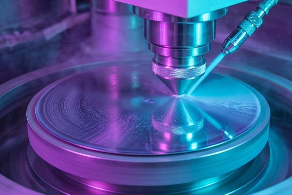
    Precision processing of a wafer surface using grinding equipment fitted with a diamond wheel

    How the precision of grinding equipment determines thickness uniformity

    To secure thickness uniformity in an actual process, the precision of the grinding equipment becomes a key variable. A grinding method that combines a high precision stage with a diamond wheel can uniformly process wafer or package surfaces down to the micron level, enabling stable achievement of target thickness across various package types such as FCBGA·WLCSP·QFN/DFN.

    What matters is whether the equipment not only grinds thinner, but also has the control capability to minimize variation throughout the grinding process. The Huvics PKG Grinder is high precision grinding equipment designed based on this principle, supporting both Full Auto and Manual Type configurations so it can be flexibly applied according to the production line scale and automation level of customers.

    The ability to maintain quality stability even under high speed process conditions and achieve high yield is an especially important criterion in mass production environments. Consistent processing capability that stays within allowable tolerances regardless of package type is the first standard to examine when selecting grinding equipment for a stacked package process.

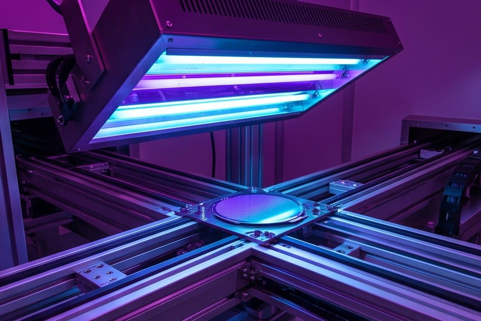
    Equipment performing UV curing on dicing tape for adhesion control and chip separation

    How lamination and UV curing connect grinding precision to yield

    If the grinding process plays the role of precisely removing thickness, then how safely chips are fixed and separated in the preceding and following stages also determines the yield of the overall process. In the tape mounting process using dicing tape, if adhesion is too strong, surface damage can occur when separating chips. Conversely, if adhesion is insufficient, chips can shift during processing and increase thickness variation.

    The key method for achieving this balance is UV curing. UV curable dicing tape weakens under controlled adhesion conditions after UV irradiation, allowing chips to be separated without damage. Furthermore, when UV curing is applied as a pretreatment before lamination, it can permanently reduce the adhesion of the dicing tape and improve the stability of subsequent processes. In this way, the timing and condition settings of UV curing are not simply an additional process, but a turning point that connects grinding precision to actual yield.

    The Huvics laminator system supports a one stop configuration that handles everything from Expander to UV Curing within a single line, and both Lamp and LED methods can be selected, enabling adhesion strength control tailored to product characteristics and process requirements. By integrating process steps, tact time is reduced, and the risk of contamination or damage that may occur during transfer between stages is also lowered. When grinding and lamination are designed as one continuous flow rather than separate processes, the meaning of securing thickness uniformity is finally completed.

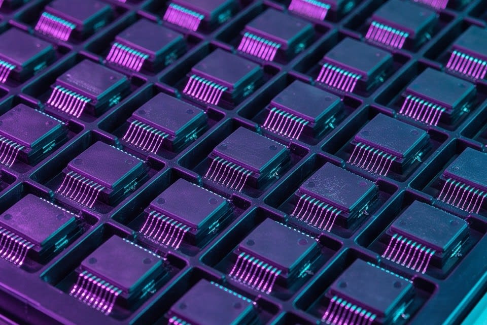
    Semiconductor packages arranged in a tray at uniform intervals and shapes

    In the era of stacked semiconductors, thickness uniformity and flatness are ultimately not issues of just one process step. Only when grinding precision, tape adhesion control, and UV curing timing work together organically can they lead to yield stability. When tracing the causes of repeated step defects and yield loss on production sites, the answer ultimately returns to how precisely these processes are connected.


    Huvics is an advanced technology company that develops and manufactures automation equipment and
    production systems across the semiconductor, LED, Mobile, and Cosmetic industries.
    With top talent and continuous technological innovation, we support customers in improving productivity and
    securing quality competitiveness.

    Huvics Contact

    Phone: 031-374-8285
    Email: cdpark@huvics.com
    Huvics Inquiry