If you are an engineer designing semiconductor packages, you have probably encountered this situation at least once. Even after carefully setting the process conditions, step differences appear between chips after stacking, and yield data begins to fall below expectations. When tracing the root cause, the issue often comes down to thickness variation and flatness control. Even though this pain point is well known, the same trial and error is often repeated on production sites.
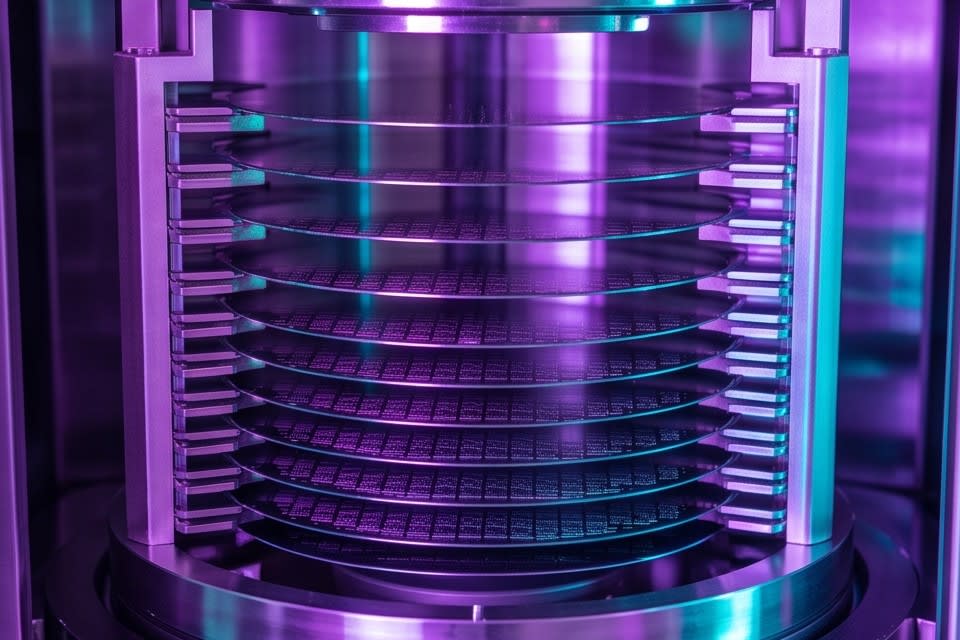
Why the shift to stacked structures made thickness control a prerequisite for the process
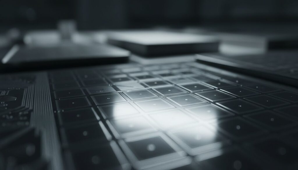
As semiconductor package structures have shifted from single layer designs to stacked architectures, the thickness and flatness of each individual chip now require a level of precision that cannot be compared with the past. In single layer structures, a certain degree of thickness variation in individual chips could be tolerated, but in 3D stacked structures where multiple chips are stacked vertically, errors in each layer accumulate, meaning even one uneven chip can compromise the reliability of the entire package.
In fact, research published on NCBI/PMC confirms that in advanced 3D stacking processes, chip thickness is reduced from around 780μm to 10μm or less, while total thickness variation TTV must be controlled to 1μm or below. As chips become thinner, the signal travel distance decreases, improving power efficiency, while lower thermal resistance also enhances heat dissipation performance.
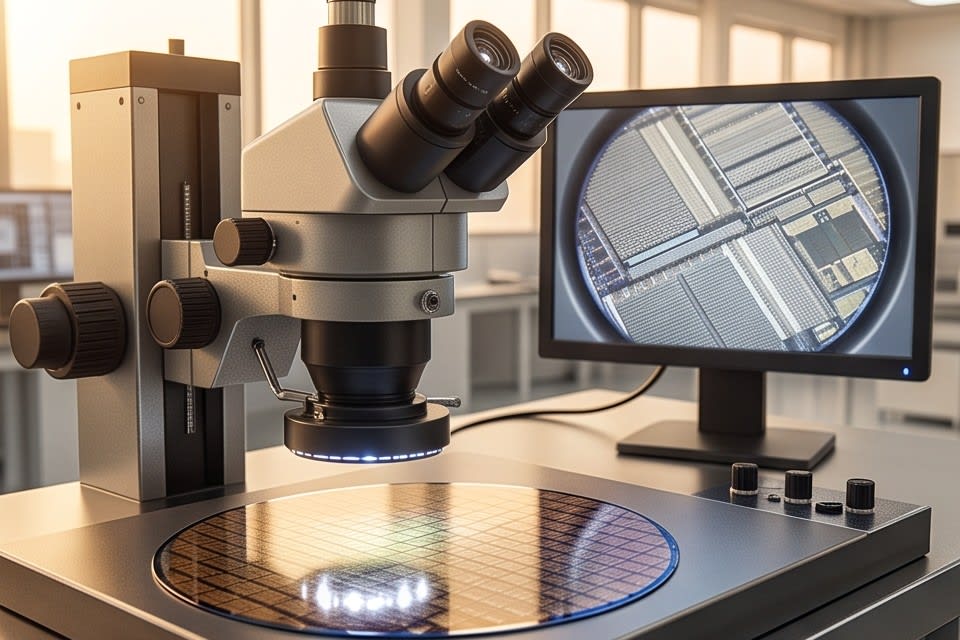
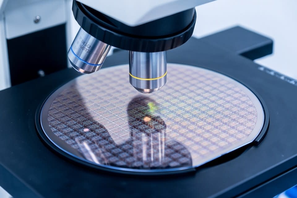
In this way, thinning is directly linked to performance improvement, but it also raises the difficulty of maintaining thickness uniformity. Micron level variation can change mechanical stress at the bonding interface after stacking and may ultimately lead to failures in long term reliability testing. As packaging technology advances, thickness control is becoming not an option, but a prerequisite for the process.
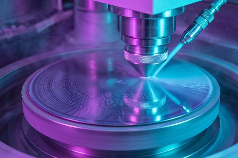
How the precision of grinding equipment determines thickness uniformity
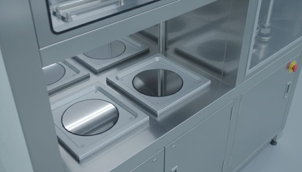
To secure thickness uniformity in an actual process, the precision of the grinding equipment becomes a key variable. A grinding method that combines a high precision stage with a diamond wheel can uniformly process wafer or package surfaces down to the micron level, enabling stable achievement of target thickness across various package types such as FCBGA·WLCSP·QFN/DFN.
What matters is whether the equipment not only grinds thinner, but also has the control capability to minimize variation throughout the grinding process. The Huvics PKG Grinder is high precision grinding equipment designed based on this principle, supporting both Full Auto and Manual Type configurations so it can be flexibly applied according to the production line scale and automation level of customers.
The ability to maintain quality stability even under high speed process conditions and achieve high yield is an especially important criterion in mass production environments. Consistent processing capability that stays within allowable tolerances regardless of package type is the first standard to examine when selecting grinding equipment for a stacked package process.
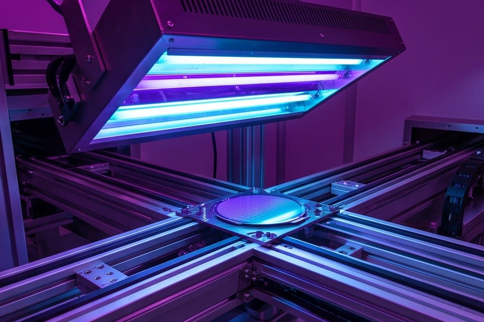
How lamination and UV curing connect grinding precision to yield
If the grinding process plays the role of precisely removing thickness, then how safely chips are fixed and separated in the preceding and following stages also determines the yield of the overall process. In the tape mounting process using dicing tape, if adhesion is too strong, surface damage can occur when separating chips. Conversely, if adhesion is insufficient, chips can shift during processing and increase thickness variation.
The key method for achieving this balance is UV curing. UV curable dicing tape weakens under controlled adhesion conditions after UV irradiation, allowing chips to be separated without damage. Furthermore, when UV curing is applied as a pretreatment before lamination, it can permanently reduce the adhesion of the dicing tape and improve the stability of subsequent processes. In this way, the timing and condition settings of UV curing are not simply an additional process, but a turning point that connects grinding precision to actual yield.
The Huvics laminator system supports a one stop configuration that handles everything from Expander to UV Curing within a single line, and both Lamp and LED methods can be selected, enabling adhesion strength control tailored to product characteristics and process requirements. By integrating process steps, tact time is reduced, and the risk of contamination or damage that may occur during transfer between stages is also lowered. When grinding and lamination are designed as one continuous flow rather than separate processes, the meaning of securing thickness uniformity is finally completed.
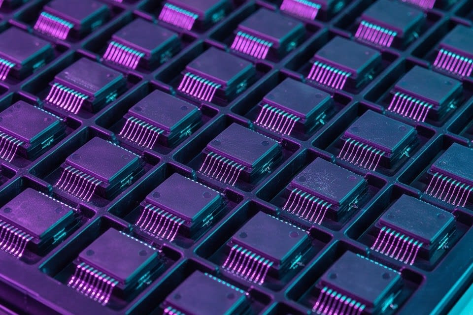
In the era of stacked semiconductors, thickness uniformity and flatness are ultimately not issues of just one process step. Only when grinding precision, tape adhesion control, and UV curing timing work together organically can they lead to yield stability. When tracing the causes of repeated step defects and yield loss on production sites, the answer ultimately returns to how precisely these processes are connected.
Huvics is an advanced technology company that develops and manufactures automation equipment and
production systems across the semiconductor, LED, Mobile, and Cosmetic industries.
With top talent and continuous technological innovation, we support customers in improving productivity and
securing quality competitiveness.
Huvics Contact
Phone: 031-374-8285
Email: cdpark@huvics.com