Tag: process innovation

  • When 1 Micron Determines Yield in the Field: Key Insights into the Chip Stacking Grinding Process

    When 1 Micron Determines Yield in the Field: Key Insights into the Chip Stacking Grinding Process

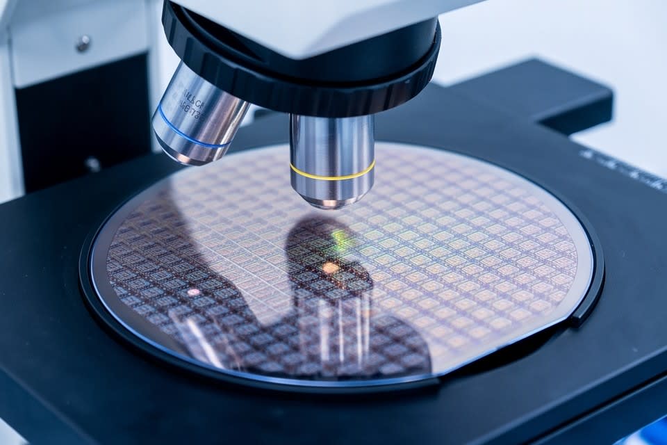
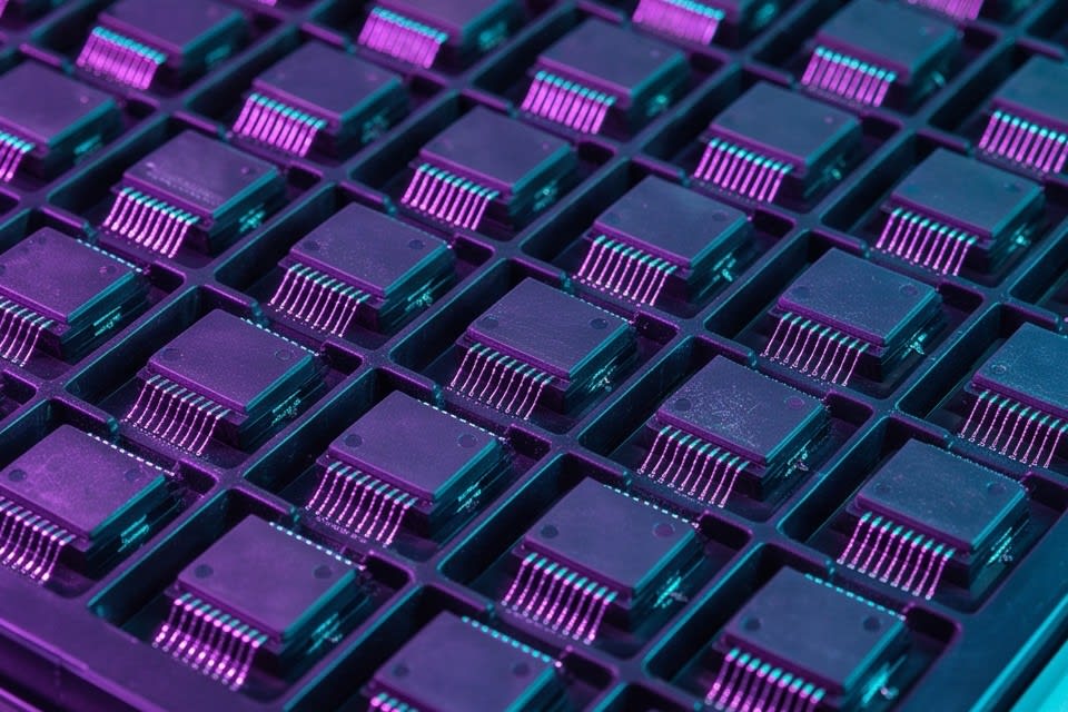
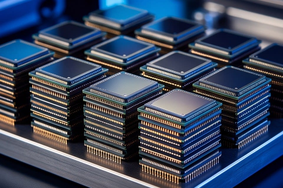
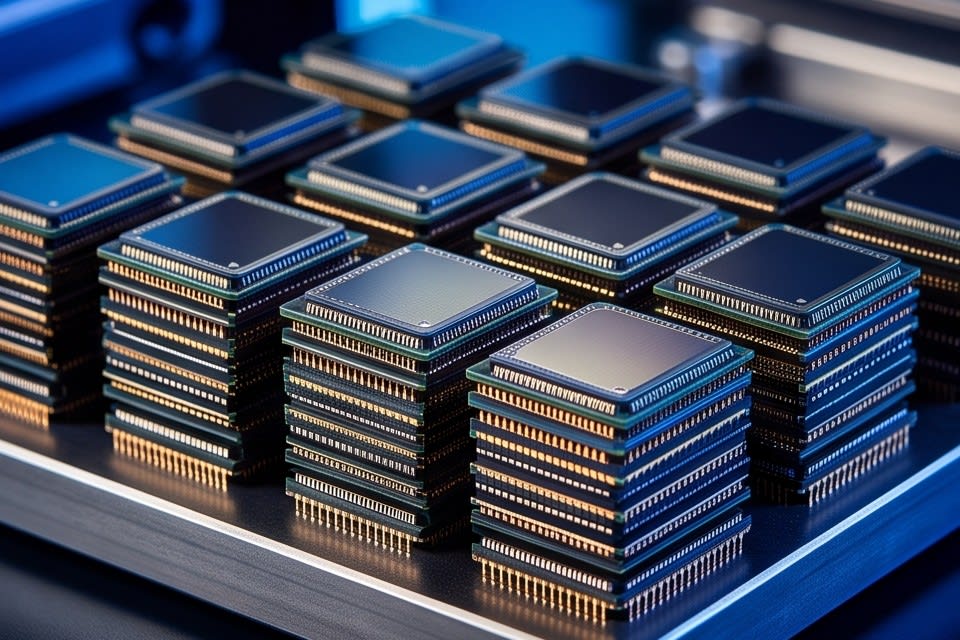
    Semiconductor chips neatly aligned and vertically stacked.

    There is a joke often shared among semiconductor design engineers. “The more chips you stack, the better, but the problem is that stacking them is far too difficult.” In real packaging processes where dozens of chip layers are stacked, the first thing to fail is not the design drawing, but flatness. In a world where a 1 micron difference can disrupt overall yield, the meaning of “grinding well” carries far more weight than expected.
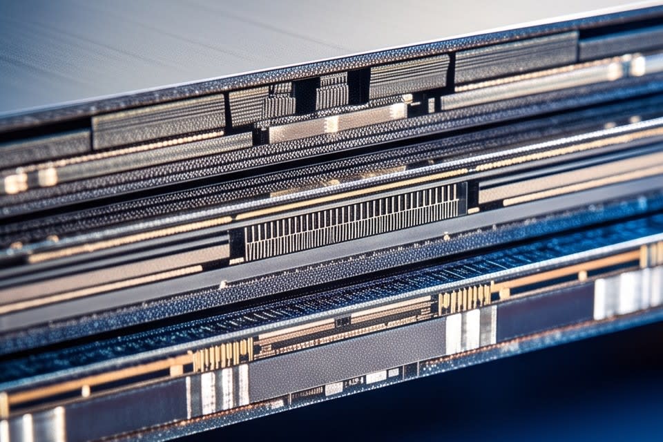
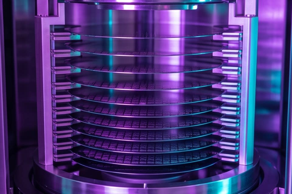
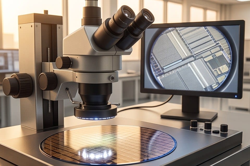
    A cross section of semiconductor chips precisely stacked with microscopic spacing.

    Why TTV Matters in Chip Stacking Structures

    In structures where chips are stacked in multiple layers, thickness variation in each layer is not just a dimensional issue. As layers accumulate, microscopic errors build up and eventually lead to electrical bonding defects or concentrated structural stress. The metric used to express this numerically is total thickness variation, or TTV.

    The TTV required in chip stacking structures is at the level of 1 micron or less, demanding precision far below one hundredth of the thickness of a human hair. If this standard is not met, bonding surfaces can lift during subsequent bonding processes or heat dissipation can become uneven, undermining the reliability of the device itself. For products such as AI semiconductors or high performance memory that vertically connect dozens of chips, the allowable variation range becomes even narrower.

    One reason TTV control is difficult in the field is the structural variables of the grinding equipment itself. The wear pattern of the grinding wheel, microscopic vibration generated during spindle rotation, and changes in the flatness of the chuck that fixes the wafer act together to make the thickness profile uneven. Uniform flatness cannot be achieved simply by turning on the equipment. How precisely these variables are controlled is the key factor that determines the yield of the entire packaging process.
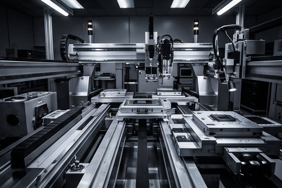
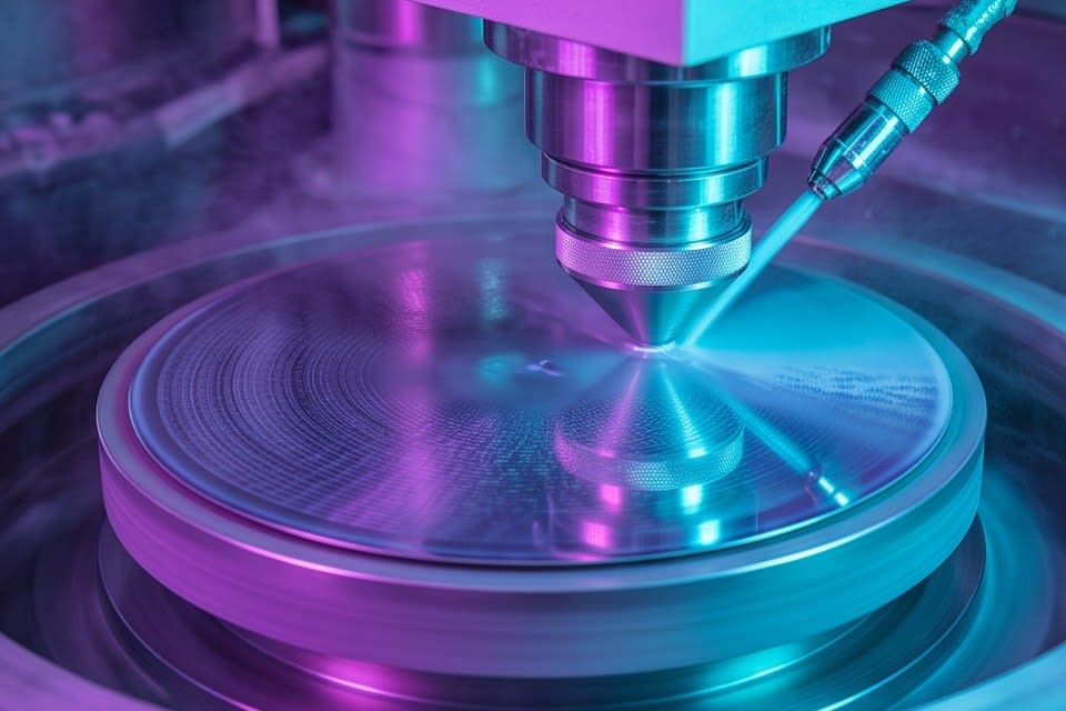
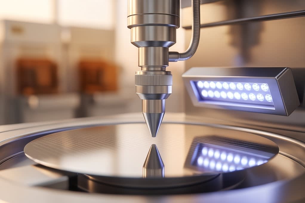
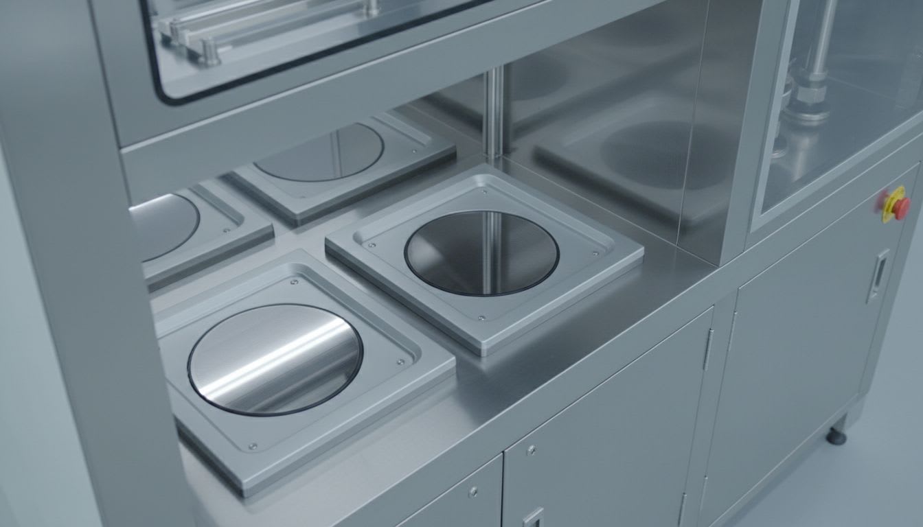
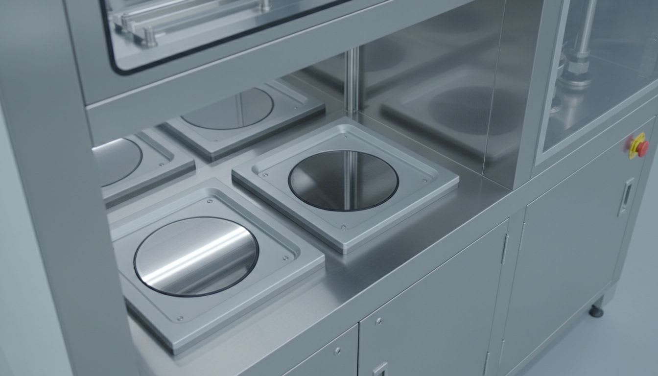
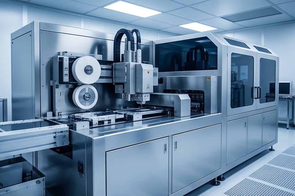
    Semiconductor process equipment equipped with a high precision stage and grinding head.

    Ultra Precision Grinding Design of the PKG Grinder

    There is a way to address this issue from the process equipment design stage. The PKG Grinder from Huvics combines a high precision stage with a diamond wheel to process various package types such as FCBGA, WLCSP, and QFN/DFN at micron level accuracy. The key is a control structure that keeps TTV variation within a defined range even during high speed processing. The TTV requirement for ultra thin wafer stacking processes is approximately 2.0 microns or less, and to meet this value reliably in a high speed grinding environment, spindle runout compensation and chuck flatness maintenance must be built into the equipment from the design stage.

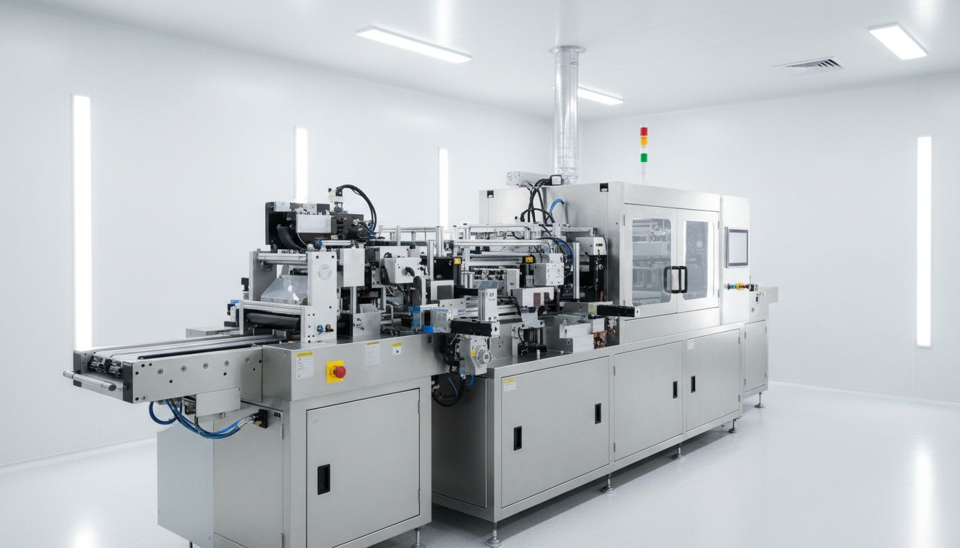
    Another practical challenge in production sites is line flexibility. In many cases, the same equipment must handle both low volume high mix processes and high volume continuous production. The option to choose Full Auto A·B types or a Manual type is a design choice made to respond to this requirement, and it directly contributes to reducing setup loss during process changeovers. Speed and uniformity are usually in conflict, but in grinding equipment, they are implemented in a way that satisfies both conditions at the same time.
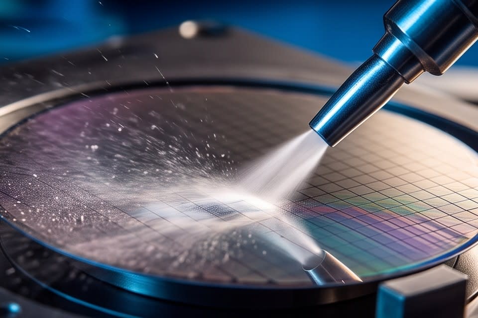
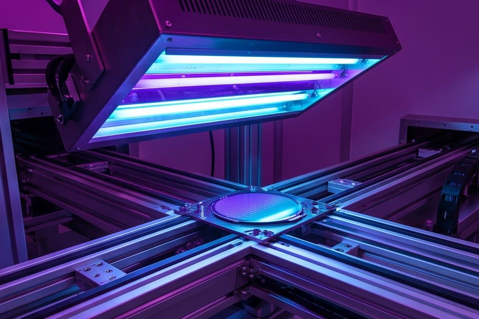
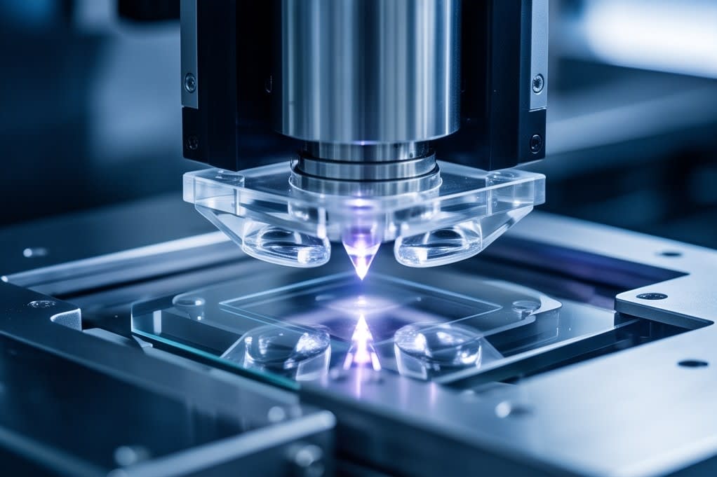
    Cleaning and drying process that removes surface residue after grinding.

    The Role of Cleaning and Drying After Grinding

    Flatness control does not end just because the grinding process is complete. Immediately after machining, grinding residue and fine particles remain on the wafer surface, and the way they are removed determines the final surface quality. This is where the choice of cleaning and drying methods becomes important.

    Comparison of Air Knife and IPA Vapor Drying

    The two drying methods mainly used in the industry are Air Knife and IPA vapor drying. Air Knife mechanically pushes liquid off the surface using a high speed gas jet, and according to research published on ResearchGate, drying within 2 seconds is possible under a speed condition of 150mm/s. In contrast, IPA vapor drying uses ultrapure isopropyl alcohol vapor to lower surface tension and guide moisture to flow away naturally without leaving marks.

    Because the two methods control processing speed and the risk of surface residue in different ways, the selection criteria vary depending on the surface characteristics of the target device and the process requirements.

    Multi Step Cleaning for Components Sensitive to Surface Contamination

    For components sensitive to surface contamination, such as camera modules, sensors, and VCM motors, a multi step cleaning approach that combines micro bubbles and water jets is becoming established.
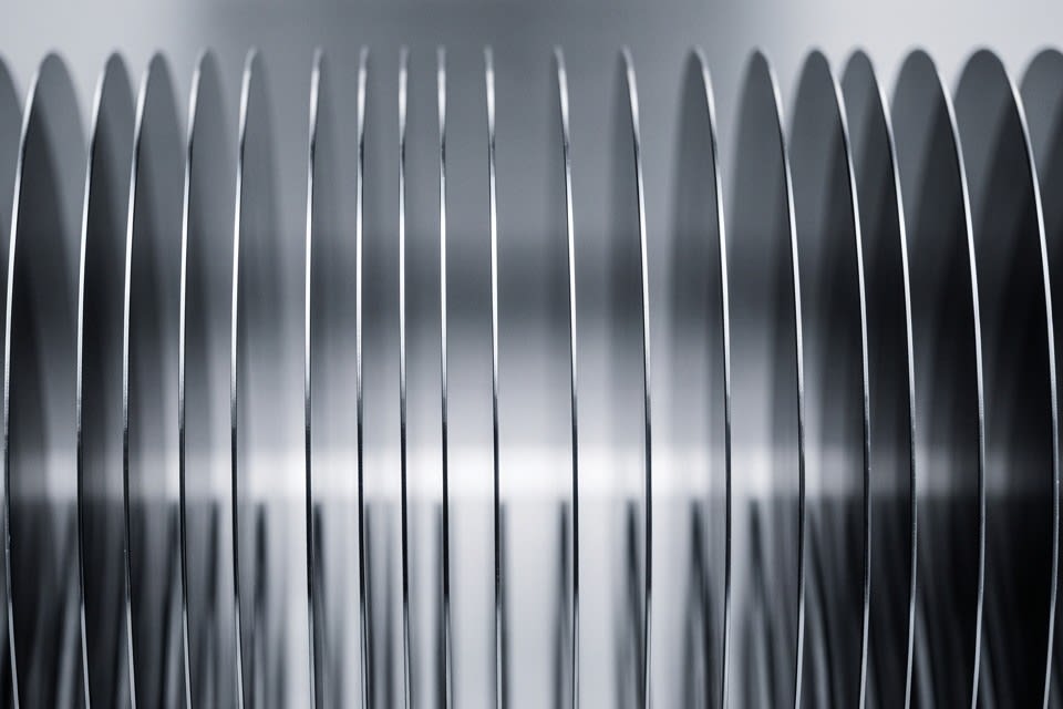
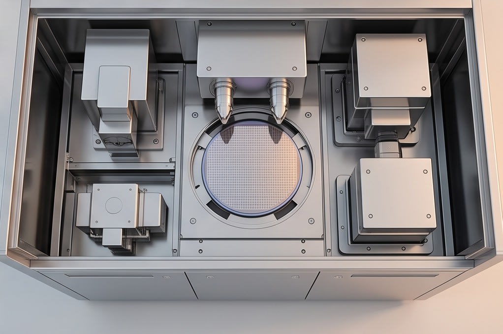
    A circular plate structure expressing the precision of the semiconductor chip stacking process.

    More than how many chips are stacked, how uniformly they are stacked determines the actual yield. From grinding precision to the selection of cleaning and drying methods, the quality of the packaging process is completed on a structure where each stage supports the next. The joke mentioned at the beginning, “stacking them is far too difficult,” turns out to describe the essence of process design quite accurately.


    Huvics is an advanced technology company that develops and manufactures automation equipment and
    production systems across the semiconductor, LED, Mobile, and Cosmetic industries.
    With top tier talent and continuous technological innovation, we support improvements in customer productivity and
    help secure quality competitiveness.

    Huvics Contact

    Phone: 031-374-8285
    Email: cdpark@huvics.com

    Contact Huvics

  • 3 Key Process Points to Reduce Defect Rates in Semiconductor Cleaning and Processing

    3 Key Process Points to Reduce Defect Rates in Semiconductor Cleaning and Processing

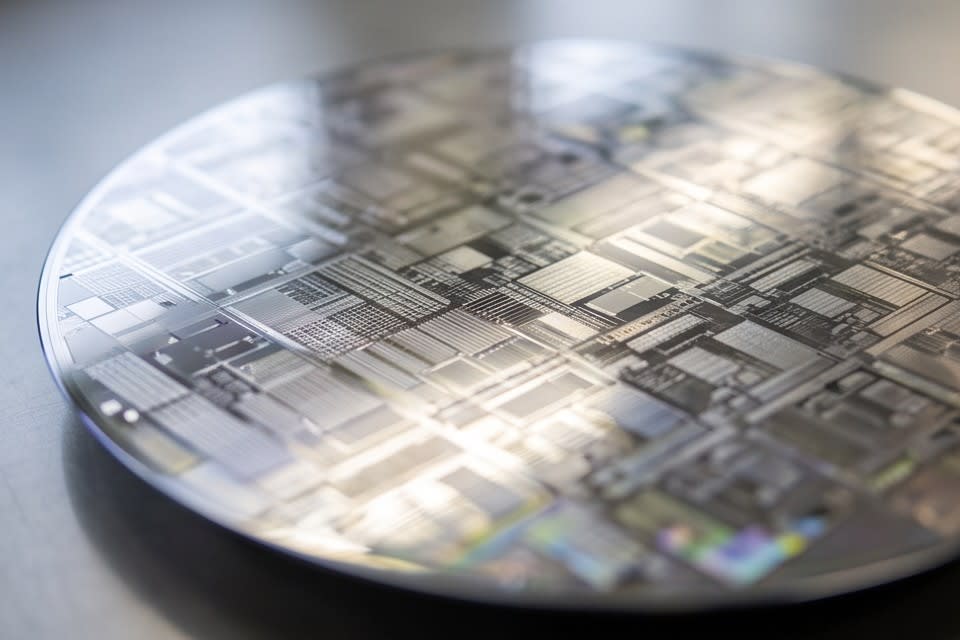
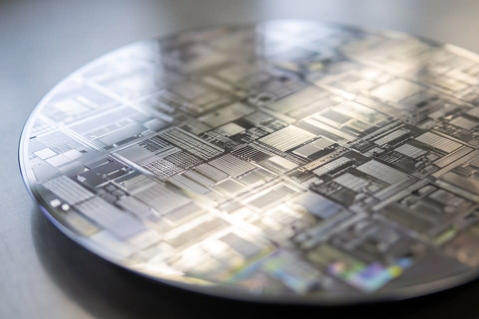
    Semiconductor wafer densely patterned with microscopic circuit lines

    As the linewidths of circuits etched onto a single semiconductor chip have narrowed to the scale of just a few nanometers, the limits of acceptable contamination in the manufacturing process have also changed. In the past, it was enough to filter out foreign matter that was difficult to detect with the naked eye. Today, even a single fine particle floating in the air can become a variable that damages an entire circuit. As processes become more precise, the standards required of cleaning equipment have risen as well, and cleaning has become a core process that determines yield, not a final step for checking quality.

    Airborne fine particles visualized and floating in laser light

    The structure in which particle contamination determines yield

    In semiconductor processes, the impact of particle contamination on yield increases sharply as process generations advance. According to Applied Physics USA, in sub-10nm processes, aerosols measuring 0.1 to 0.5 micrometers are considered among the greatest risk factors, and even a single 10nm particle can cause a short circuit or structural deformation in a transistor.

    The reality that even within the same production line, yield can vary between 95% and 75% depending on the level of particle contamination control shows that the cleaning process is not simply a matter of hygiene. As miniaturization progresses, the tolerance for contamination becomes narrower, and how precisely foreign matter is removed in the early stages of the process effectively determines the quality of the final product. This is why cleaning equipment is no longer a lower priority in process design, but has moved to the center of yield strategy.

    As particle size becomes smaller, the precision required to detect and remove those particles also increases. Process miniaturization is changing the very criteria used to select equipment.

    Dynamic bubbles formed as water droplets fall

    Principles and field application of multi stage cleaning technology

    The performance of cleaning equipment depends on how contamination particles are separated from the surface. Micro bubble cleaning removes particles with shock waves generated when bubbles tens of micrometers in size collapse near the surface. In a study published in the Korean Journal of Chemical Engineering, a maximum jet flow velocity of 148.5mm/s was confirmed in a micro cylinder array structure, and this level of flow velocity is effective for removing fine contaminants with strong surface adhesion.

    Nanobubble technology uses bubbles smaller than 5nm to reach even finer particles, and because the bubbles remain stable for a long time, cleaning efficiency is maintained even on complex surface structures.

    Engineers handling components with different shapes in the field, such as camera modules, sensors, VCM motors, and trays, understand that it is difficult to process every product with a single method. This is why multi stage cleaning structures that combine Micro Bubble, Water Jet, and Air Knife are chosen for actual production lines.

    The drying process, which completely removes residual moisture after cleaning, must also be integrated into a single flow to reduce the risk of foreign matter reattaching between processes. Designing cleaning and drying as one continuous system has become essential for securing quality stability.

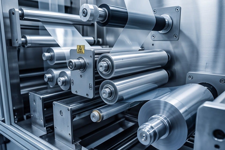
    Drive unit of lamination equipment where tape is supplied through rollers

    Thickness uniformity and process integration determine defect rates

    To reduce defects in the package processing stage, the first requirement is to clearly define the criteria for selecting equipment. The allowable range of total thickness variation, TTV, required in high performance packaging is typically 0.5 to 2.0 micrometers, and this standard becomes even stricter for products that stack chips in multiple layers, such as AI semiconductors and high performance memory.

    Huvics takes an approach that structurally reduces defect factors occurring after cleaning through its PKG Grinder and Laminator System. The PKG Grinder uses a high precision stage and diamond wheel to uniformly process various packages, including FCBGA, WLCSP, QFN, and DFN, at the micron level, and its core role is to keep thickness variation within the allowable range. The Laminator System handles tape attachment and curing processes from Expander to UV Curing within a single line, reducing contamination and alignment errors that can occur during movement between processes.

    Cases in which defects in semiconductor tape bonding processes or foreign matter issues in camera modules were resolved through cleaning and integrated process design show that equipment selection goes beyond simply comparing specifications. As stacking becomes deeper and package structures become more complex, thickness uniformity and process continuity act as the criteria that determine defect rates. The answer to what it means for final yield to reduce variables at a specific process stage is already embedded in the equipment design.

    Precision automation equipment organically arranged at a semiconductor production site

    As semiconductor processes become more precise, the role of cleaning and processing equipment is shifting from simple support to the center of yield management. In an environment where the size of a single contamination particle can affect overall yield, the principle used to remove particles and the method used to control thickness variation become the practical standards for equipment selection. As the pace of process miniaturization accelerates, the importance of equipment that meets these standards will continue to grow.


    Huvics is an advanced technology company that develops and manufactures automation equipment and
    production systems across the semiconductor, LED, Mobile, and Cosmetic industries.
    With top talent and continuous technological innovation, Huvics supports customers in improving productivity and
    securing quality competitiveness.

    Huvics Contact

    Phone: 031-374-8285
    Email: cdpark@huvics.com
    Huvics Inquiry

  • How to Manage Grinding, Lamination, and UV Curing Stages to Improve Chip Stacking Yield

    How to Manage Grinding, Lamination, and UV Curing Stages to Improve Chip Stacking Yield

    A detailed inspection of a semiconductor wafer surface using optical equipment

    If you are an engineer designing semiconductor packages, you have probably encountered this situation at least once. Even after carefully setting the process conditions, step differences appear between chips after stacking, and yield data begins to fall below expectations. When tracing the root cause, the issue often comes down to thickness variation and flatness control. Even though this pain point is well known, the same trial and error is often repeated on production sites.

    Multiple wafers vertically aligned and stacked

    Why the shift to stacked structures made thickness control a prerequisite for the process

    As semiconductor package structures have shifted from single layer designs to stacked architectures, the thickness and flatness of each individual chip now require a level of precision that cannot be compared with the past. In single layer structures, a certain degree of thickness variation in individual chips could be tolerated, but in 3D stacked structures where multiple chips are stacked vertically, errors in each layer accumulate, meaning even one uneven chip can compromise the reliability of the entire package.

    In fact, research published on NCBI/PMC confirms that in advanced 3D stacking processes, chip thickness is reduced from around 780μm to 10μm or less, while total thickness variation TTV must be controlled to 1μm or below. As chips become thinner, the signal travel distance decreases, improving power efficiency, while lower thermal resistance also enhances heat dissipation performance.

    In this way, thinning is directly linked to performance improvement, but it also raises the difficulty of maintaining thickness uniformity. Micron level variation can change mechanical stress at the bonding interface after stacking and may ultimately lead to failures in long term reliability testing. As packaging technology advances, thickness control is becoming not an option, but a prerequisite for the process.

    Precision processing of a wafer surface using grinding equipment fitted with a diamond wheel

    How the precision of grinding equipment determines thickness uniformity

    To secure thickness uniformity in an actual process, the precision of the grinding equipment becomes a key variable. A grinding method that combines a high precision stage with a diamond wheel can uniformly process wafer or package surfaces down to the micron level, enabling stable achievement of target thickness across various package types such as FCBGA·WLCSP·QFN/DFN.

    What matters is whether the equipment not only grinds thinner, but also has the control capability to minimize variation throughout the grinding process. The Huvics PKG Grinder is high precision grinding equipment designed based on this principle, supporting both Full Auto and Manual Type configurations so it can be flexibly applied according to the production line scale and automation level of customers.

    The ability to maintain quality stability even under high speed process conditions and achieve high yield is an especially important criterion in mass production environments. Consistent processing capability that stays within allowable tolerances regardless of package type is the first standard to examine when selecting grinding equipment for a stacked package process.

    Equipment performing UV curing on dicing tape for adhesion control and chip separation

    How lamination and UV curing connect grinding precision to yield

    If the grinding process plays the role of precisely removing thickness, then how safely chips are fixed and separated in the preceding and following stages also determines the yield of the overall process. In the tape mounting process using dicing tape, if adhesion is too strong, surface damage can occur when separating chips. Conversely, if adhesion is insufficient, chips can shift during processing and increase thickness variation.

    The key method for achieving this balance is UV curing. UV curable dicing tape weakens under controlled adhesion conditions after UV irradiation, allowing chips to be separated without damage. Furthermore, when UV curing is applied as a pretreatment before lamination, it can permanently reduce the adhesion of the dicing tape and improve the stability of subsequent processes. In this way, the timing and condition settings of UV curing are not simply an additional process, but a turning point that connects grinding precision to actual yield.

    The Huvics laminator system supports a one stop configuration that handles everything from Expander to UV Curing within a single line, and both Lamp and LED methods can be selected, enabling adhesion strength control tailored to product characteristics and process requirements. By integrating process steps, tact time is reduced, and the risk of contamination or damage that may occur during transfer between stages is also lowered. When grinding and lamination are designed as one continuous flow rather than separate processes, the meaning of securing thickness uniformity is finally completed.

    Semiconductor packages arranged in a tray at uniform intervals and shapes

    In the era of stacked semiconductors, thickness uniformity and flatness are ultimately not issues of just one process step. Only when grinding precision, tape adhesion control, and UV curing timing work together organically can they lead to yield stability. When tracing the causes of repeated step defects and yield loss on production sites, the answer ultimately returns to how precisely these processes are connected.


    Huvics is an advanced technology company that develops and manufactures automation equipment and
    production systems across the semiconductor, LED, Mobile, and Cosmetic industries.
    With top talent and continuous technological innovation, we support customers in improving productivity and
    securing quality competitiveness.

    Huvics Contact

    Phone: 031-374-8285
    Email: cdpark@huvics.com
    Huvics Inquiry

  • How Grinding Process Uniformity Determines AI Semiconductor Packaging Yield

    How Grinding Process Uniformity Determines AI Semiconductor Packaging Yield

    Optical equipment inspecting fine surface conditions and uniformity in the semiconductor packaging process

    There is one fact that only some people in the semiconductor industry know. The factor that determines the performance of cutting-edge AI chips is not the design or the material, but ‘is hidden in the uniformity of the grinding process’, which is difficult to see with the naked eye. Over time, a yield gap that is difficult to close emerges between sites that understand this fact and those that do not.

    Fine structure of a vertically stacked 3D semiconductor chip cross section

    Why thickness uniformity and flatness determine yield

    In the packaging of AI semiconductors and high-performance memory semiconductors, thickness uniformity and flatness are not simple dimensional requirements. In a 3D stacked structure where chips are stacked vertically, the surface condition of each layer directly determines the bonding quality of the upper and lower layers. According to a technical report by Applied Materials, the uniformity of the wafer surface directly affects stacking yield, reliability, and electrical performance, and even slight surface variations can degrade bonding quality.

    As the number of stacked layers increases, these requirements become even stricter. According to industry discussions reported by TrendForce, the current thickness standard for HBM4, fourth-generation high-bandwidth memory, is 775 micrometers, and raising it to the 825~900 micrometer level is being considered for next-generation HBM4E and HBM5. As technology evolves toward stacking more chips higher, how precisely the flatness of each layer is controlled determines the reliability of the entire package.

    A single thickness error can distort the path of an electrical signal, and that leads to yield loss. This is why ultra-precision processing becomes a prerequisite, not an option, and standards for equipment that meets these requirements are also rising.

    Grinding equipment that uniformly processes the wafer surface through a combination of a high-precision stage and a diamond wheel

    Ultra-precision grinding technology of the PKG Grinder

    Huvics PKG Grinder is high-precision grinding equipment designed to respond to these strict standards. By combining a high-precision stage with a diamond wheel, it enables thickness processing at the micron level and can be applied to various package types, including FCBGA, flip chip ball grid array, WLCSP, wafer level chip scale package, QFN·DFN, and solar cells.

    What is highly valued on production sites is not only its high precision, but also the fact that it maintains stable quality even in high-speed processes and achieves high yield. Depending on the characteristics of the production line, users can choose from fully automated, Full Auto, A type·B type and Manual types, making it flexible for both high-mix low-volume lines and high-volume continuous production lines. For packages that require micron-level precision, the repeatability of equipment determines yield, and whether that repeatability can be maintained even under high-speed conditions is the key factor in equipment selection.

    An operator managing an automated process site through a conveyor system in a cleanroom environment

    The relationship between process automation and cost control

    On the production floor, the impact of equipment selection on the cost structure is greater than many expect. In the industry, unplanned downtime in semiconductor manufacturing lines is known to cause losses of more than 260,000 dollars per hour, and even the same repair is reported to cost 3~5 times more in an unplanned situation than when handled during scheduled maintenance. This is why equipment stability and maintenance predictability become financial decision criteria beyond simple operational convenience.

    The same logic applies to the cleaning process. A method that combines micro bubbles, water jets, and air knives in stages for cleaning various components such as camera modules, sensors, VCM motors, and trays is an approach that removes contamination particles and lowers defect rates in a single process. The laminator system also integrates everything from lamination to UV curing into one flow, reducing process steps and shortening tact time.

    The direction of integrating processes and raising the level of automation is ultimately the way to secure both predictable quality and cost control, and its significance is confirmed in the actual numbers from production sites.

    A stacked semiconductor chip with fine interconnections precisely bonded together

    The precision requirements for AI semiconductor packaging will continue to rise. In this trend, which equipment is used and how processes are configured determine not only current yield, but also the capability to handle next-generation products. The fact that a single grinding process holds the reliability of the entire package is why precision processing equipment deserves attention in this market.


    Huvics is an advanced technology company that develops and manufactures automation equipment and
    production systems across the semiconductor, LED, mobile, and cosmetics industries.
    With top talent and continuous technological innovation, we support customers in improving productivity and
    securing quality competitiveness.

    Huvics Contact

    Telephone: 031-374-8285
    Email: cdpark@huvics.com

    Huvics Inquiry

  • The Value of Precision Cleaning in Semiconductor Yield and the Process Innovation Strategy of the Huvics One Stop Laminator

    The Value of Precision Cleaning in Semiconductor Yield and the Process Innovation Strategy of the Huvics One Stop Laminator

    Huvics

    An industry saying states that the success or failure of semiconductor manufacturing is determined not at the beginning of a massive process, but by the level of cleanliness at the final stage. Today, that message carries even greater weight. At a time when even invisible microscopic contamination can undermine the reliability of an entire product, precision cleaning has become the final safeguard that determines production yield, going far beyond a simple auxiliary measure.

    To block unnecessary exposure within complex assembly lines and reach the highest level of manufacturing efficiency, we will explore how the process integration strategy presented by the Huvics one stop laminator system can resolve chronic bottlenecks in semiconductor manufacturing sites and maximize competitiveness.

    Integrated Laminator Solution by Huvics

    The Importance of Precision Cleaning in Determining Semiconductor Yield

    Core Value in Back End Processes

    The semiconductor manufacturing process is often described as a continuous series of fine processes, but in reality, the back end stage at the peak of that process is the most sensitive section that determines yield. Just before a wafer fully takes shape as a chip, the introduction of even a single microscopic contaminant can cause critical damage to the reliability of the entire product.

    For this reason, today precision cleaning systems have become a core process that fundamentally blocks defect factors and guarantees final product quality, rather than merely serving as an auxiliary method for removing foreign substances. In increasingly complex and sophisticated semiconductor structures, it is no exaggeration to say that cleanliness in the final stage is the last line of defense for measuring product completeness.

    Strengthening Production Efficiency and Competitiveness

    In particular, at sites where advanced equipment such as the Huvics one stop laminator is introduced, precision cleaning acts as a solution that removes chronic bottlenecks in the manufacturing process. This process goes beyond maintaining cleanliness and becomes a pivotal point that makes the entire production line flow more flexibly and dramatically improves final yield.

    Only chips completed in the cleanest possible state can meet the strict requirements of the market, and this precision cleaning strategy becomes the most reliable foundation for maintaining manufacturing competitiveness in the rapidly changing global semiconductor market.

    Core of Precision Cleaning and Curing Processes

    Technological Innovation of the Huvics One Stop Laminator

    Perfect Control of Potential Risk Factors

    The reason the Huvics precision cleaning system receives outstanding evaluations in the field is that it goes beyond the technical level of removing visible foreign substances. Inside the manufacturing environment, microscopic defect factors that are difficult to detect with the naked eye are constantly present, and the Huvics system detects these potential risk factors in advance and prevents them before they occur, ensuring product quality uniformity at a level close to perfection.

    The core technologies implemented by Huvics in the latest semiconductor assembly lines are as follows.

    • Improving process efficiency by applying an LED based UV curing process
    • Operating the precision cleaning process and UV curing stage in an organically integrated manner

    Process Efficiency Through Integrated Equipment

    In the past, each process was separated, resulting in frequent product movement, and the gaps and unnecessary exposure generated during that movement often caused takt time delays and potential contamination. However, Huvics has overcome these physical limitations by processing everything from tape mounting to expander operation and precise UV curing within a single piece of equipment.

    This integrated method, which controls residues in real time and achieves optimal adhesion strength, strengthens product durability while minimizing unnecessary movement, thereby maximizing process stability. From the producer perspective, it provides a powerful tool to minimize the probability of defects even within complex assembly stages, which directly leads to a dramatic improvement in overall production efficiency.

    Huvics is proving directly in the field that precision cleaning is a core strategic asset that supports the stability of the entire manufacturing process, going beyond simple cleanliness maintenance.

    Precise Design of the Huvics System

    A Strategic Choice for Manufacturing Innovation

    Ultimately, the competitiveness of semiconductor manufacturing depends not on the act of cleaning chips itself, but on how perfectly invisible uncertainty can be controlled. True manufacturing innovation begins only when precision cleaning is redefined from a simple maintenance concept into a strategic asset that integrates the process flow and secures quality uniformity.

    As proven by the integrated equipment of Huvics, the choice to transform process complexity into efficient simplicity will become the most powerful weapon for protecting irreplaceable quality value in a rapidly changing market. Now is the time to remove the invisible contamination factors hidden in your production line and experience a higher level of yield completeness.


    Huvics is an advanced technology company that develops and manufactures automation equipment and
    production systems across the semiconductor, LED, Mobile, and Cosmetic industries.
    With top talent and continuous technological innovation, we support customers in improving productivity and
    securing quality competitiveness.

    Huvics Contact Information

    Phone: 031-374-8285
    Email: cdpark@huvics.com

    Huvics Inquiry

  • Huvics 4-Stage Cleaning and Drying System Captures Global Market Attention – A Defect-Free Quality Solution for Semiconductors and Precision Parts

    Huvics 4-Stage Cleaning and Drying System Captures Global Market Attention – A Defect-Free Quality Solution for Semiconductors and Precision Parts

    Huvics

    In semiconductor and ultra-precision parts manufacturing, even a single microscopic contaminant can become a critical variable that determines the success or failure of the entire process. Today, when product perfection directly translates into corporate competitiveness, the global market is focusing on perfect cleaning as the engineering answer to achieving defect-free quality.

    Huvics meets the strict demands of these advanced industries and sets a new standard through its distinctive 4-stage cleaning and drying system, which extends from microbubbles to water jets, air knives, and precision oven drying. Let us take a closer look behind this innovative process and see why manufacturing sites around the world choose Huvics solutions and trust its technological expertise.

    Huvics precision cleaning equipment

    Huvics, an Essential Solution for Advanced Manufacturing Sites

    The Core of the 4-Stage Cleaning and Drying System

    In the semiconductor and precision parts industries, cleanliness goes beyond simply maintaining product appearance and becomes a core factor that determines product viability. In advanced manufacturing environments where one tiny particle or invisible contaminant can affect the defect rate of an entire process, perfect cleaning is directly linked to corporate competitiveness.

    Huvics deeply understands these industrial demands and has built the following distinctive 4-stage cleaning and drying system.

    • Separation of microscopic contaminants using microbubbles
    • Powerful removal of foreign matter through water jets
    • Precision surface treatment with air knife technology
    • Removal of residual moisture through precision oven drying

    By perfectly separating and removing even invisible microscopic contaminants, this system has earned strong trust across the industry.

    Huvics cleaning system structure

    Blocking Residual Moisture and Ensuring Quality Stability

    The Huvics approach does not stop at simply wiping away foreign matter. Through the precision oven drying function built into the system, residual moisture immediately after cleaning is dried at once, securing a technological advantage that fundamentally blocks corrosion and quality degradation factors that may be caused by moisture.

    This consistent process treatment prevents unexpected quality defects that may occur during subsequent processes and greatly contributes to productivity improvement at manufacturing sites. If defect-free quality is the most important value in the semiconductor and ultra-precision parts fields today, Huvics presents the most reliable engineering answer for achieving that defect-free quality.

    advanced robotic cleaning process

    Technology Trusted by the Global Market

    Strict Quality Standards and Field Suitability

    The reason Huvics is recognized in the global market for its unmatched technological capability is that it has consistently met the extremely strict quality standards required by the electronics industry. Especially in advanced fields such as autonomous driving sensors and camera modules, where even the smallest error cannot be tolerated, a minor product defect can lead directly to a critical safety issue.

    Huvics cleaning solutions have become core infrastructure that guarantees both efficiency and product stability in processes requiring this extreme level of precision. Field engineers trust the Huvics system for the following reasons.

    • Consideration of harsh field environments from the design stage
    • Consistent cleaning performance maintained even after long operation
    • Technological capability that enables process standardization

    Ultimately, defect-free quality is a non-negotiable standard in the semiconductor and ultra-precision parts industries, and the Huvics 4-stage cleaning and drying system is the most engineering-based and reliable answer for achieving that strict standard. Just as true trust is built when technology proves strong results in real field environments, Huvics will continue to serve as a reliable partner that drives customer success and presents a new standard for advanced industries.


    Huvics is an advanced technology company that develops and manufactures automation equipment and
    production systems across the semiconductor, LED, Mobile, and Cosmetic industries.
    With top talent and continuous technological innovation, we support customers in improving productivity and
    securing quality competitiveness.

    Huvics Contact

    Phone: 031-374-8285
    Email: cdpark@huvics.com
    Huvics inquiry

  • Huvics One Stop Laminator System-Innovative Technology That Enhances Semiconductor Process Efficiency and Quality

    Huvics One Stop Laminator System-Innovative Technology That Enhances Semiconductor Process Efficiency and Quality

    Huvics

    In semiconductor manufacturing, even a one-second delay is not simply a loss of time. It is the beginning of a critical bottleneck that can determine a company’s overall competitiveness. On an assembly line where countless processes work together like gears, the inconvenience of handling tape mounting and UV curing separately has long been a persistent challenge that undermines production efficiency.

    Can we connect this complex process flow seamlessly into one unified system and achieve both productivity and quality at the same time? Discover why the global market is paying attention to the Huvics One Stop Laminator System, and the innovative solution that will shape the future of semiconductor processing.

    Huvics One Stop Laminator System

    Innovation of the Huvics One Stop Laminator

    Solving Bottlenecks Through Process Integration

    In semiconductor manufacturing, productivity is a key indicator that directly determines corporate competitiveness. On a semiconductor assembly line where countless processes are interconnected, even minor waiting time between processes can lead to a critical bottleneck that reduces overall efficiency.

    Huvics focused precisely on this point and fundamentally redesigned the once complex workflow. The innovative One Stop Laminator System, which combines tape mounting and UV curing technology into one integrated solution, is becoming the answer that resolves long-standing challenges for semiconductor manufacturers in a single step.

    The cumbersome process of the past, in which products had to pass through an expander and then be moved again to UV curing equipment, has now been fully integrated within the Huvics system. By organically processing previously separate operations within a single system, workflow has become much smoother and overall tact time has been noticeably reduced.

    The strategic advantages offered by the Huvics system are as follows.

    • Fundamentally resolves bottlenecks in manufacturing sites
    • Maximizes flexibility through process integration within a single system
    • Reduces overall tact time through improved workflow

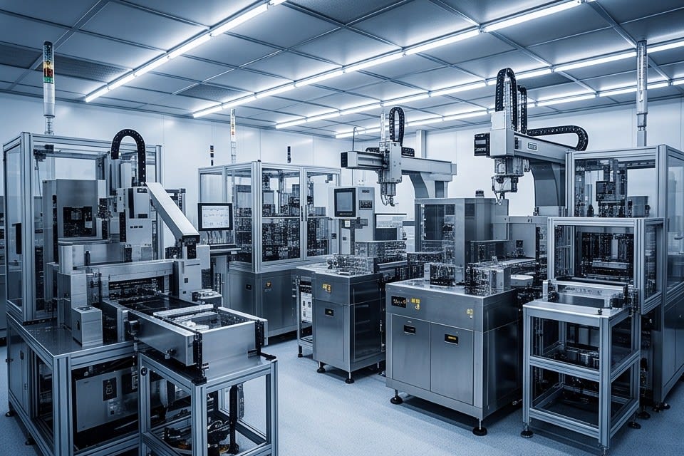
    Optimized automated production line

    Precision Process Control and Quality Competitiveness

    Technical Completeness and Global Quality Standards

    The decisive reason Huvics continues to earn unwavering trust from leading semiconductor manufacturers around the world lies in its uncompromising precision process control capabilities. In semiconductor assembly, a momentary variation can create major differences in results, making equipment precision more important than anything else.

    In particular, the LED-based precision UV curing technology that Huvics proudly offers precisely achieves the optimal adhesive strength for each product. This technology thoroughly blocks subtle quality variables that can easily arise during assembly and helps maintain unwavering consistency even amid minor changes in the manufacturing environment.

    This level of technical completeness goes beyond simply reducing defect rates. It becomes a solid foundation for fully meeting the strict standards of global markets that demand exceptional quality. Achieving both production efficiency and quality at the same time is never easy, but Huvics has made it a reality by building its own technological moat.

    Strategy for Securing Process Stability

    Adopting the Huvics system means securing process stability and committing to quality competitiveness that remains steady even in the constantly changing semiconductor market. The reasons Huvics has established a strong position as a trusted partner at global manufacturing sites are as follows.

    1. Maintaining a commitment to precision and technical integrity
    2. Fully satisfying the strict quality standards of the global market
    3. Securing competitiveness by building a proprietary technological moat

    Close-up of precision UV curing process

    Solving complex bottlenecks in semiconductor manufacturing and redefining quality standards through uncompromising precision are the fundamental reasons Huvics continues to earn unwavering trust in the global market. This innovative integrated system that maximizes process efficiency goes beyond being a tool that simply reduces work time. It becomes a key choice for companies seeking stable competitiveness in the rapidly changing semiconductor market.

    The technological capability of Huvics, built by insisting on precision at every moment and enhancing process stability, will now become a reliable partner that leads your manufacturing site to stronger and more complete results.


    Huvics is an advanced technology company that develops and manufactures automation equipment and
    production systems across the semiconductor, LED, Mobile, and Cosmetic industries.
    With outstanding professionals and continuous technological innovation, Huvics supports customers in improving productivity and
    securing quality competitiveness.

    Huvics Contact Information

    Phone: 031-374-8285
    Email: cdpark@huvics.com
    Huvics Inquiry

  • Huvics Micron-Level Ultra-Precision Package Grinding Technology Beyond Global Standards

    Huvics Micron-Level Ultra-Precision Package Grinding Technology Beyond Global Standards

    Huvics

    As the performance of semiconductors and IT devices advances dramatically, package grinding technology, which now determines manufacturing yield, has evolved beyond a simple repetitive process into a core capability that defines the overall perfection of a product. As devices become smaller and more powerful, the space occupied by semiconductor chips continues to shrink, while the amount of information they must process grows exponentially.

    In this environment, Huvics is perfectly solving the demanding challenges of ultra-thinning and high performance in manufacturing sites through micron-level ultra-precision machining technology. We aim not only to maintain technological superiority, but also to present a new standard for the future semiconductor industry. The fine and precise differences we create will ultimately become the most solid and powerful foundation that enables your products to deliver overwhelming value in the market.

    Huvics package grinder equipment

    Core Capabilities of Huvics Package Grinding

    Optimization Technology for Each Package Type

    The unrivaled performance delivered by the Huvics Package Grinder (PKG Grinder) begins with insight that responds flexibly to the constantly changing semiconductor package environment. The differentiated capabilities of Huvics are as follows.

    • Precisely analyzes the characteristics of each package type, from FCBGA to WLCSP
    • Possesses the technical capability to identify optimized processing conditions for each package type
    • Maintains thickness uniformity and flatness at the highest level in core processes
    • Plays a key role in maximizing semiconductor reliability and stability after processing

    Precision Control That Elevates Quality Completion

    This goes beyond simply meeting the specifications required in industrial sites. It is a process of completing the level of quality that directly affects the actual product life and final performance. By insisting on these invisible and subtle differences to the very end, Huvics helps customers experience results that exceed the most demanding standards required by the market.

    The overwhelming process precision we have built becomes a reliable technical guarantee that allows your semiconductors to maintain peak performance at all times.

    high-precision stage and grinding wheel

    Technological Innovation for Ultra-Precision Machining

    High-Precision Stage and Diamond Wheel

    The key secret unique to Huvics that enables this ultra-precision machining lies in the perfect integration of high-precision stage and diamond wheel technology. Actual semiconductor production sites inevitably face the challenges of minute vibrations and numerous variables due to high-speed operating environments. However, the Huvics system confidently overcomes these limitations and ensures unwavering, consistent quality.

    Production Efficiency and Technical Support

    For global manufacturers that must maximize production efficiency, process stability is directly linked to strong market competitiveness. That is why our technology becomes the most reliable partner for sites seeking higher yield. Huvics goes one step further by not merely complying with existing global standards, but by changing the paradigm of semiconductor production through continuous technological innovation.

    What we provide for customers’ successful mass production is not simply equipment, but definite and sophisticated technical support that clearly solves the complex and difficult equation of yield.

    precision data analysis by expert personnel

    Partnership for Global Competitiveness

    Process Precision and Innovative Change

    As a result, every process with Huvics delivers the most efficient and precise results, driving innovative change that reshapes the landscape of global manufacturing competition. Many companies struggle to improve yield, but the true difference depends on how precisely thickness is controlled at the final stage of the process.

    We test the limits of technology and surpass them every time, supporting our customers’ products so they can be recognized for the highest quality in markets around the world.

    Working Together for Sustainable Growth

    The technology of Huvics goes beyond simply supplying manufacturing equipment. It is a partnership for success that helps customer businesses achieve sustainable growth. Even at this moment, we are listening closely to the subtle signals from the field and building the most precise and powerful technical foundation so that your products can lead the future IT world.

    With Huvics, your products will prove an overwhelming difference in quality that competitors can never match.

    advanced automated process system

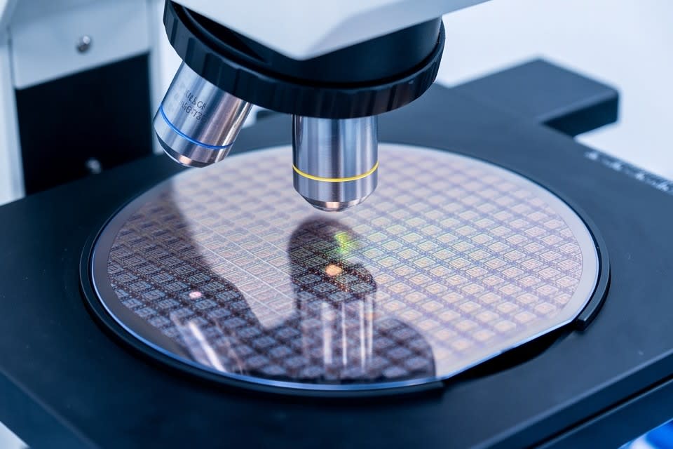
    ultra-precision grinding technology

    semiconductor package with perfect quality


    Huvics is an advanced technology company that develops and manufactures automation equipment and
    production systems across the semiconductor, LED, mobile, and cosmetics industries.
    With top talent and continuous technological innovation, we support customer productivity improvement and
    quality competitiveness.

    Huvics Contact

    Phone: 031-374-8285
    Email: cdpark@huvics.com
    Huvics inquiry