Tag: yield management

  • How to Manage Grinding, Lamination, and UV Curing Stages to Improve Chip Stacking Yield

    How to Manage Grinding, Lamination, and UV Curing Stages to Improve Chip Stacking Yield

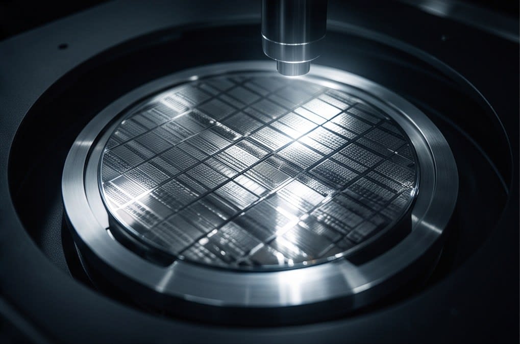
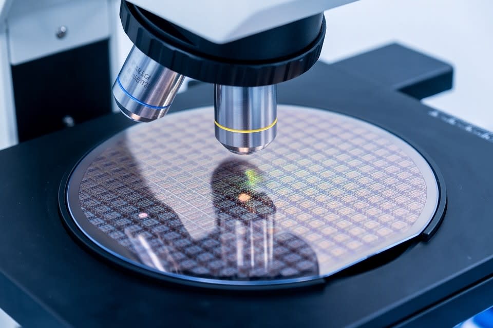
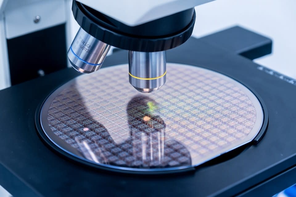
    A detailed inspection of a semiconductor wafer surface using optical equipment

    If you are an engineer designing semiconductor packages, you have probably encountered this situation at least once. Even after carefully setting the process conditions, step differences appear between chips after stacking, and yield data begins to fall below expectations. When tracing the root cause, the issue often comes down to thickness variation and flatness control. Even though this pain point is well known, the same trial and error is often repeated on production sites.
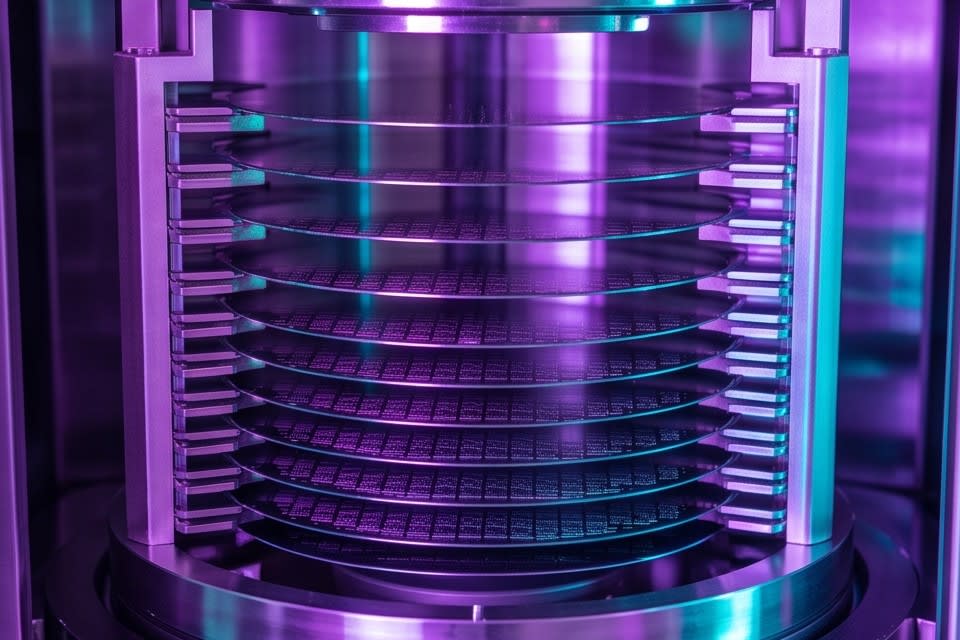
    Multiple wafers vertically aligned and stacked

    Why the shift to stacked structures made thickness control a prerequisite for the process

    As semiconductor package structures have shifted from single layer designs to stacked architectures, the thickness and flatness of each individual chip now require a level of precision that cannot be compared with the past. In single layer structures, a certain degree of thickness variation in individual chips could be tolerated, but in 3D stacked structures where multiple chips are stacked vertically, errors in each layer accumulate, meaning even one uneven chip can compromise the reliability of the entire package.

    In fact, research published on NCBI/PMC confirms that in advanced 3D stacking processes, chip thickness is reduced from around 780μm to 10μm or less, while total thickness variation TTV must be controlled to 1μm or below. As chips become thinner, the signal travel distance decreases, improving power efficiency, while lower thermal resistance also enhances heat dissipation performance.

    In this way, thinning is directly linked to performance improvement, but it also raises the difficulty of maintaining thickness uniformity. Micron level variation can change mechanical stress at the bonding interface after stacking and may ultimately lead to failures in long term reliability testing. As packaging technology advances, thickness control is becoming not an option, but a prerequisite for the process.
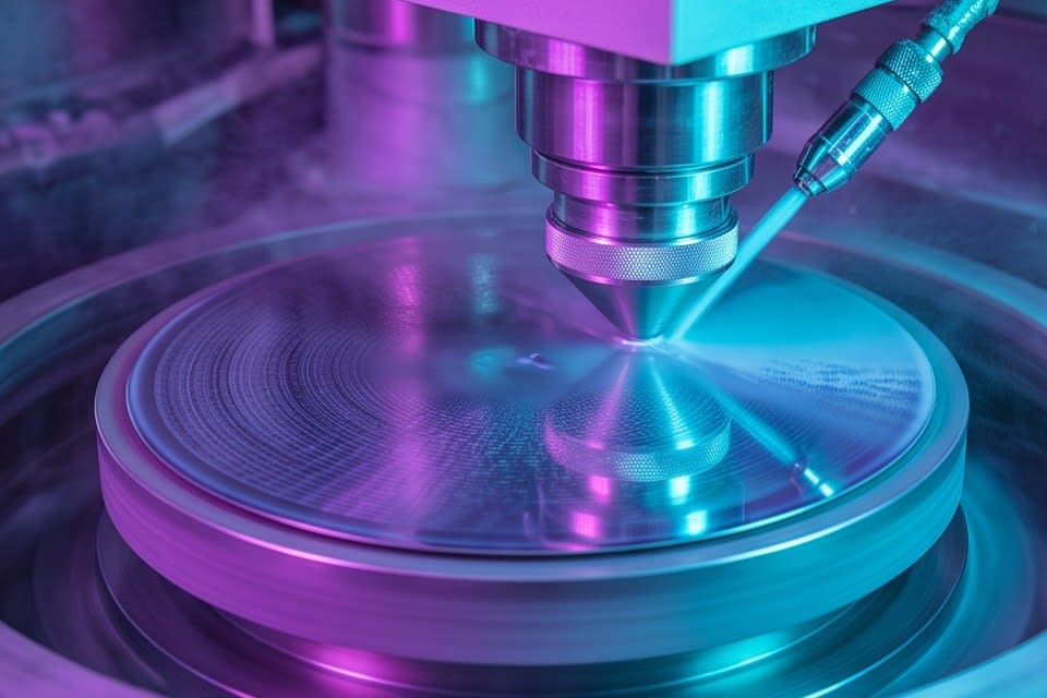
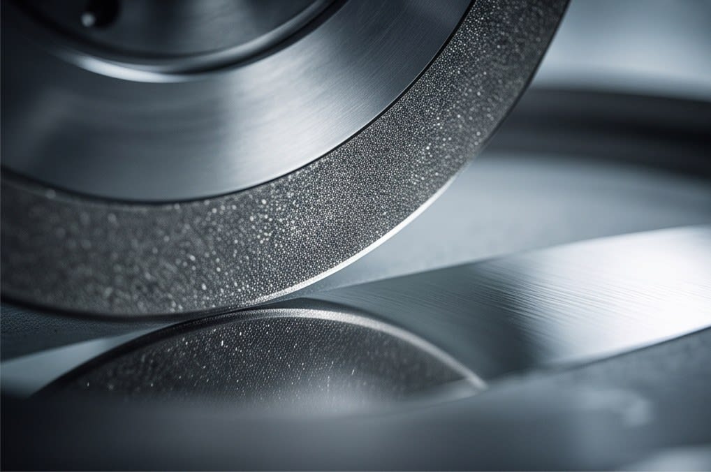
    Precision processing of a wafer surface using grinding equipment fitted with a diamond wheel

    How the precision of grinding equipment determines thickness uniformity

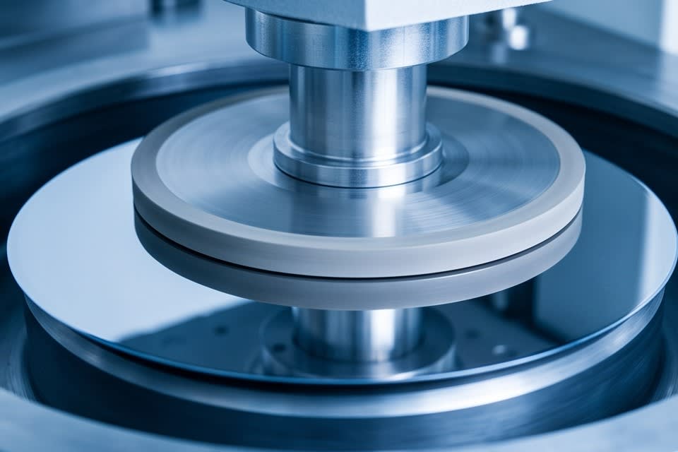
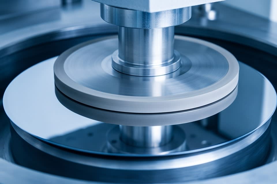
    To secure thickness uniformity in an actual process, the precision of the grinding equipment becomes a key variable. A grinding method that combines a high precision stage with a diamond wheel can uniformly process wafer or package surfaces down to the micron level, enabling stable achievement of target thickness across various package types such as FCBGA·WLCSP·QFN/DFN.

    What matters is whether the equipment not only grinds thinner, but also has the control capability to minimize variation throughout the grinding process. The Huvics PKG Grinder is high precision grinding equipment designed based on this principle, supporting both Full Auto and Manual Type configurations so it can be flexibly applied according to the production line scale and automation level of customers.

    The ability to maintain quality stability even under high speed process conditions and achieve high yield is an especially important criterion in mass production environments. Consistent processing capability that stays within allowable tolerances regardless of package type is the first standard to examine when selecting grinding equipment for a stacked package process.
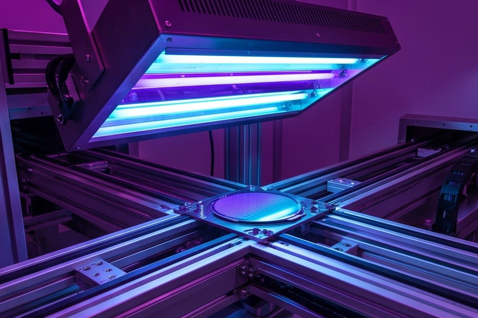
    Equipment performing UV curing on dicing tape for adhesion control and chip separation

    How lamination and UV curing connect grinding precision to yield

    If the grinding process plays the role of precisely removing thickness, then how safely chips are fixed and separated in the preceding and following stages also determines the yield of the overall process. In the tape mounting process using dicing tape, if adhesion is too strong, surface damage can occur when separating chips. Conversely, if adhesion is insufficient, chips can shift during processing and increase thickness variation.

    The key method for achieving this balance is UV curing. UV curable dicing tape weakens under controlled adhesion conditions after UV irradiation, allowing chips to be separated without damage. Furthermore, when UV curing is applied as a pretreatment before lamination, it can permanently reduce the adhesion of the dicing tape and improve the stability of subsequent processes. In this way, the timing and condition settings of UV curing are not simply an additional process, but a turning point that connects grinding precision to actual yield.

    The Huvics laminator system supports a one stop configuration that handles everything from Expander to UV Curing within a single line, and both Lamp and LED methods can be selected, enabling adhesion strength control tailored to product characteristics and process requirements. By integrating process steps, tact time is reduced, and the risk of contamination or damage that may occur during transfer between stages is also lowered. When grinding and lamination are designed as one continuous flow rather than separate processes, the meaning of securing thickness uniformity is finally completed.
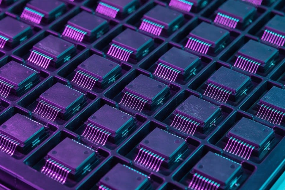
    Semiconductor packages arranged in a tray at uniform intervals and shapes

    In the era of stacked semiconductors, thickness uniformity and flatness are ultimately not issues of just one process step. Only when grinding precision, tape adhesion control, and UV curing timing work together organically can they lead to yield stability. When tracing the causes of repeated step defects and yield loss on production sites, the answer ultimately returns to how precisely these processes are connected.


    Huvics is an advanced technology company that develops and manufactures automation equipment and
    production systems across the semiconductor, LED, Mobile, and Cosmetic industries.
    With top talent and continuous technological innovation, we support customers in improving productivity and
    securing quality competitiveness.

    Huvics Contact

    Phone: 031-374-8285
    Email: cdpark@huvics.com

    Huvics Inquiry

  • How Are You Managing the Grinding, Lamination, and Cleaning Processes That Determine Semiconductor Yield

    How Are You Managing the Grinding, Lamination, and Cleaning Processes That Determine Semiconductor Yield

    Grinding equipment for controlling minute thickness variations in semiconductor wafers

    When working on a semiconductor line, even a single thickness deviation can bring down an entire day of yield. The process design is correct, and the equipment is operating normally, yet the finished thickness varies little by little. If this subtle difference is ignored, it returns as a bigger issue in the next process, and correcting it requires stopping the entire line. Even though this situation repeats itself, many sites still run the same process in the same way.

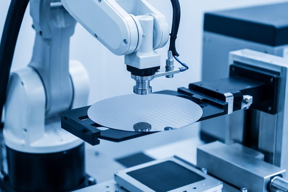
    An automated robot arm precisely handling a wafer

    Why Thickness Uniformity Determines the Yield of Stacked Packages

    In structures where dozens of chips are stacked vertically, such as AI semiconductors and high-performance memory, thickness variation in each layer is not merely a dimensional issue. As layers are stacked, deviations accumulate, and the reliability of the final package is directly affected by that accumulated value.

    According to industry standards, the allowable range for thickness uniformity in production wafers is around 0.5~2.0 micrometers, and fields that require high precision, such as 5G processors and AI accelerators, require control within 0.3 micrometers. Standards stating that tolerance must remain within 1 micrometer even when the final thickness is reduced to around 20 micrometers are also being applied in actual processes.

    To implement this level of precision reliably, both the stage precision of grinding equipment and the control level of the diamond wheel must be supported together. Maintaining uniform package thickness goes beyond improving the completeness of a specific process and becomes a prerequisite that determines the yield of all subsequent assembly stages. As the number of stacked layers increases, managing variation in the initial grinding stage is becoming a decisive factor in the quality of the entire process.

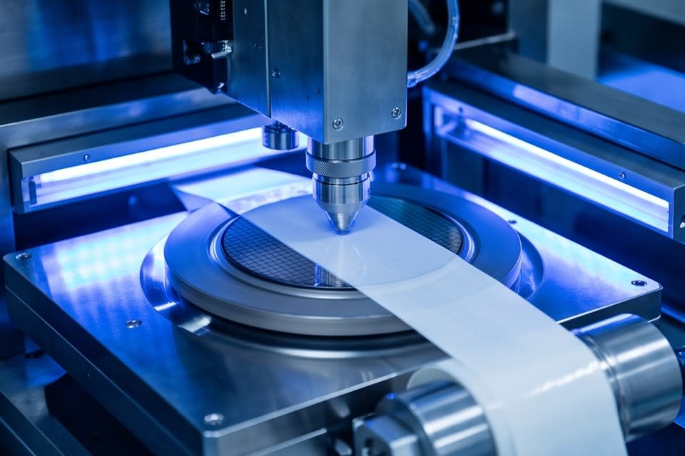
    An automated system precisely attaching tape onto a wafer

    How an Integrated Laminator Structure Reduces Process Bottlenecks

    When tape mounting and UV curing are operated as separate processes on the manufacturing floor, transfer time and waiting sections occur between the two pieces of equipment, and quality variables can enter during that gap. The more separated the processes are, the more management points are created, and it becomes harder to identify where bottlenecks occur.

    The integrated laminator structure, which processes everything from expansion to UV curing within a single line, emerged as a way to solve this issue. Huvics’ one-stop laminator system combines tape mounting and UV curing into one continuous flow, eliminating transfer sections between processes and reducing overall takt time. The LED-based UV curing method maintains stable adhesive strength while preventing adhesive defects that may occur during complex packaging assembly processes.

    In the industry, comparative analyses indicate that inline UV curing systems are more efficient in high-capacity continuous production environments that require throughput of more than 500 units per hour. A structure that provides both Semi Auto and Manual options makes it possible to configure the line flexibly according to product type and production scale. How simply the process is designed becomes the key decision criterion for improving both yield and productivity.

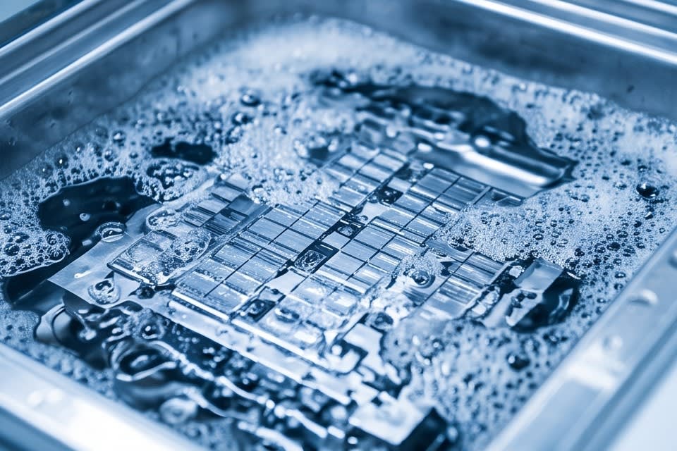
    A component being immersed and cleaned in liquid where fine bubbles are generated

    Why the Precision of Cleaning Technology Becomes the First Line of Defense for Final Quality

    For components where surface cleanliness is directly linked to performance, such as camera modules and autonomous driving sensors, even a microscopic particle invisible to the naked eye can lead to a defect judgment. In semiconductor tray cleaning processes as well, residual contaminants repeatedly become sources of contamination in the next process.

    Huvics’ cleaning system uses a multi-stage structure that combines microbubbles, water jets, and air knives step by step, sequentially treating contaminants with various properties that are difficult to remove with a single cleaning method. In the industry, research findings have accumulated showing that micro- and nanobubble cleaning technology using bubbles with a diameter of 0.1 micrometers or less is effective in removing organic matter from semiconductor surfaces, and there are also cases where particle removal efficiency of 92.5% was confirmed in jet flow cleaning using acoustic bubble array technology.

    As the applications are diverse, including camera modules, sensors, VCM motors, and trays, the system is designed for process completeness by incorporating an oven drying function that removes residual moisture after cleaning. Configurations with Full Auto and Manual options make it possible to adjust the automation level and maintenance method to suit the production environment.

    Although cleaning may appear to be the final process, field data repeatedly confirms that its results become the first line of defense for final quality. This is where the precision of technology that captures a single particle determines the meaning of finished product reliability.

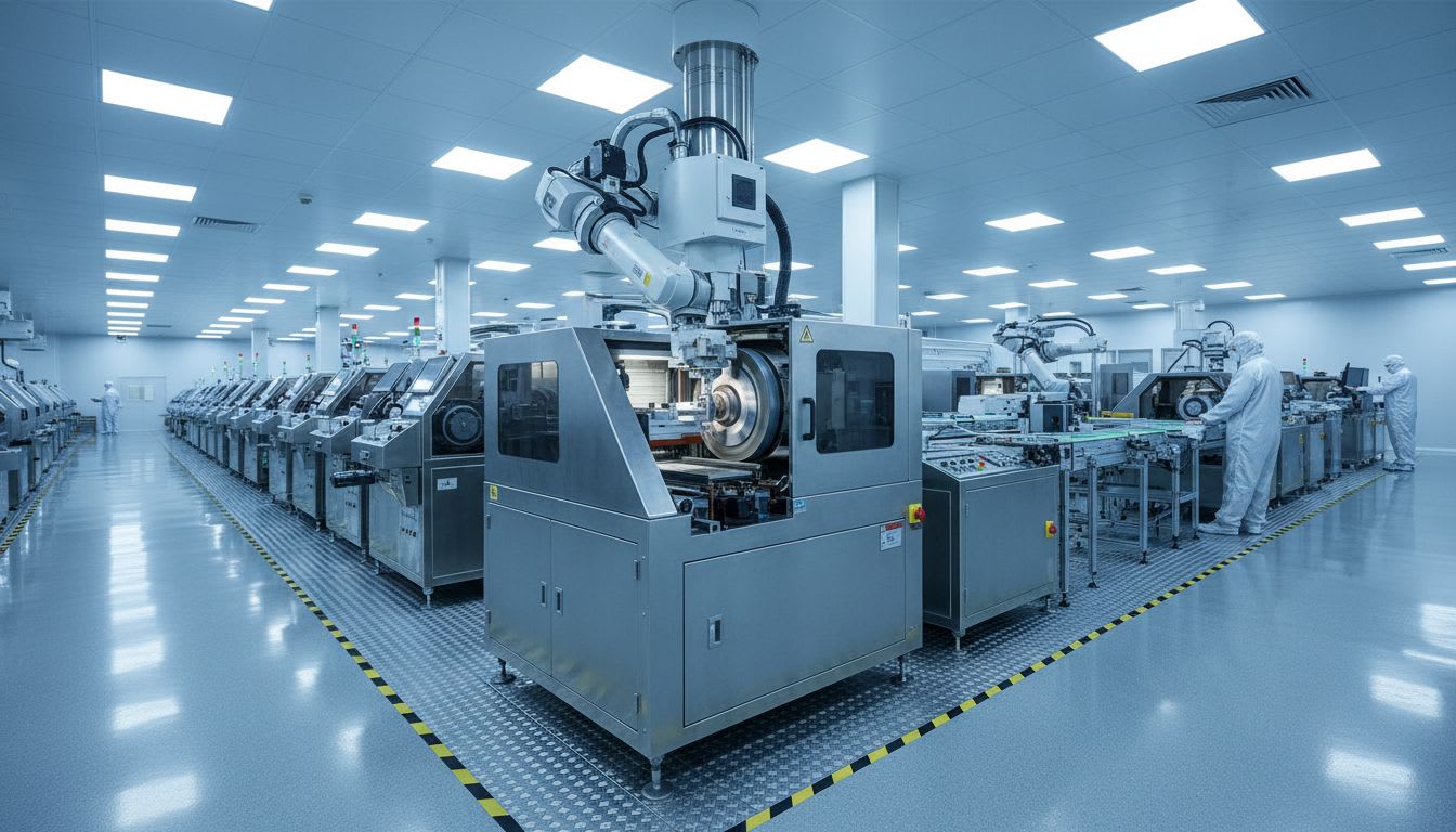
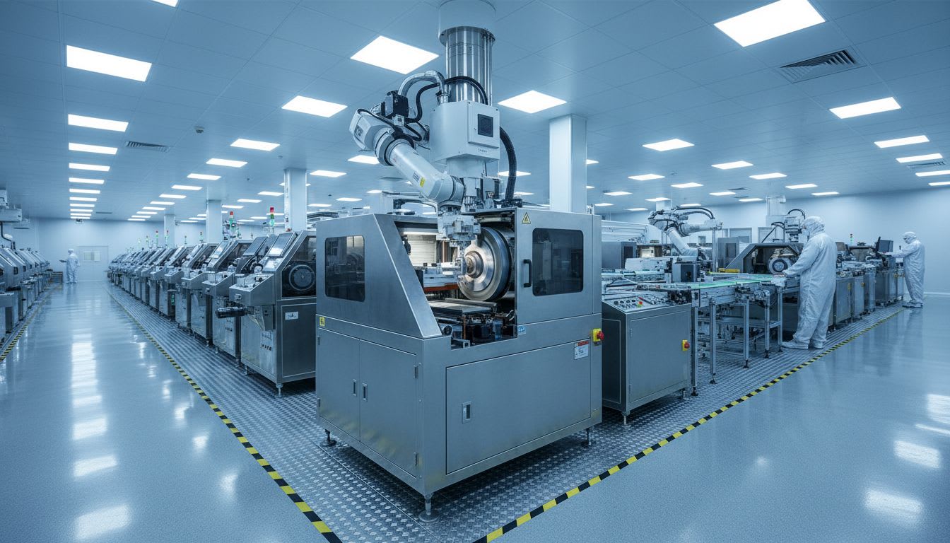
    A manufacturing site where various types of equipment are arranged in a row

    The minute thickness deviation that first caused the line to stop is, in fact, not a gap in process design but the result of precision levels at each stage failing to work together. When grinding uniformity, lamination integration efficiency, and multi-stage cleaning completeness are connected as one flow, the causes of repeated defects finally disappear. The industrial standard created by ultra-precision machining is determined not by the performance of a single piece of equipment, but by how tightly the entire process is connected.


    Huvics is an advanced technology company that develops and manufactures automation equipment and
    production systems across the semiconductor, LED, Mobile, and Cosmetic industries.
    With top talent and continuous technological innovation, we support customers in improving productivity and
    securing quality competitiveness.

    Huvics Contact

    Phone: 031-374-8285
    Email: cdpark@huvics.com
    Huvics Inquiry

  • The Core of Next-Generation Semiconductor Packaging-Ultra-Precision Grinding Solutions Implemented with Huvics PKG Grinder

    The Core of Next-Generation Semiconductor Packaging-Ultra-Precision Grinding Solutions Implemented with Huvics PKG Grinder

    Huvics

    As next-generation artificial intelligence and high-performance memory semiconductors reshape the industrial landscape, the completeness of the ultra-precision process that can flawlessly bring these designs to life is just as important as design innovation itself. No matter how advanced a chip may be, tiny thickness deviations or flatness imbalances that occur during production can become critical obstacles that lower product yield and erode competitiveness.

    This is why engineers in the field work tirelessly in demanding process environments where even the slightest vibration cannot be tolerated. The time has come when technical support capable of controlling even micron-level errors is essential, beyond simple manufacturing processes. Let us take a closer look at how the ultra-precision grinding solution presented by Huvics addresses production floor challenges and sets a new standard for semiconductor processes.

    Advanced semiconductor packaging process cleanroom

    Technical Standards of the Semiconductor Packaging Process

    As the next-generation artificial intelligence and high-performance memory semiconductor industry expands at an unprecedented pace, the technical standards required in semiconductor packaging processes are also rising to levels beyond imagination. Controlling micron-level errors has now become an absolute benchmark that determines the market competitiveness of a product, beyond simple technological advantage.

    The Importance of Advanced Packaging and Precision

    Especially when dealing with advanced packaging technologies such as flip chip ball grid array(FCBGA) or wafer level chip scale package(WLCSP), even the most innovative design becomes ineffective if extremely precise thickness uniformity and near-perfect flatness cannot be secured. To dramatically enhance process completeness in these ultra-precision environments, Huvics presents the following solutions.

    • Securing process stability through a high-precision stage
    • Integration of proprietary diamond wheel technology
    • Setting a new industry standard through PKG Grinder

    Precision robotic arm and automated process

    Operational Efficiency and Stability of PKG Grinder

    The true differentiator of the Huvics PKG Grinder equipment lies in its ability to maximize practical operational efficiency on the production floor, beyond precision alone. The sophisticated combination of a high-precision stage and advanced diamond wheel technology provides powerful stability that does not allow even the slightest vibration that may occur during microprocess operations. This becomes the key driving force that dramatically reduces product defect rates and enables the ultimate manufacturing goal of high-yield production.

    Flexible Response Through Field-Customized Design

    In addition, it supports the following customized designs in consideration of the different scales and operating methods of each production site.

    • Implementation of automated processes through a full auto system
    • Support for manual types optimized for field conditions
    • Establishment of a flexible response system for changing market conditions

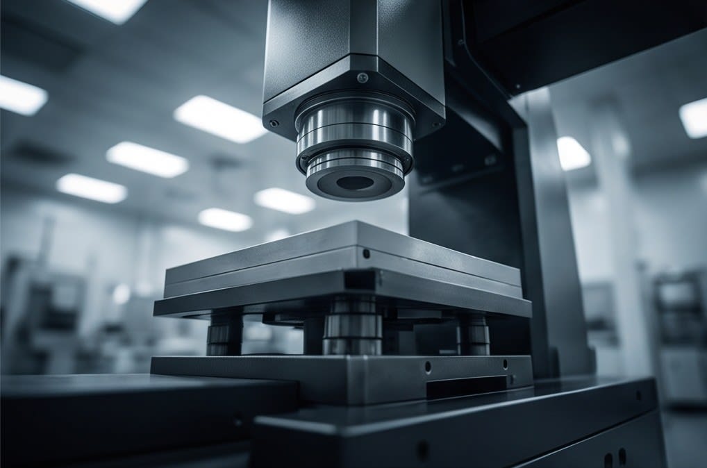
    Vertical descent of an ultra-precision grinding head

    Securing Technological Advantage and Quality Competitiveness

    In the increasingly complex semiconductor packaging market, the combination of technological advantage and customized solutions becomes a powerful answer to eliminating the uncertainty that companies face. Maintaining consistent quality in harsh, high-speed process environments is not easy, but the technology of Huvics makes it possible. Since precision cleaning and grinding processes are the final stages of semiconductor manufacturing, even a small difference in this process determines the overall completeness and lifespan of the product.

    A Strategic Choice for the Next-Generation Semiconductor Market

    The Huvics PKG Grinder supports the realization of the highest quality based on unwavering technology and expertise, helping customers move beyond process limitations and become leaders in the next-generation semiconductor market. Process optimization built on this trust will become the most reliable strategic choice for companies to secure overwhelming quality competitiveness and promote long-term growth amid intense technological competition.

    Close-up of diamond wheel particles

    Future Value of Ultra-Precision Process Infrastructure

    Ultimately, to lead the competition in next-generation technology, it is more important than anything else to go beyond designing high-performance chips and secure an ultra-precision process infrastructure that can implement them perfectly. Through its unparalleled precision cleaning and grinding technologies that detect even invisible microscopic errors, Huvics helps customers achieve both improved production yield and faster market response at the same time.

    The First Step Toward Leadership in Future Semiconductor Technology

    Reviewing and optimizing the grinding solution that forms the foundation of the current process is truly the wise first step toward securing leadership in future semiconductor technology. Huvics will continue to stand with all customers who seek to overcome the limitations of semiconductor packaging processes, fully applying all of its technological assets to firmly support innovation in the field.

    Semiconductor wafer undergoing the grinding process

    Small differences measured in microns come together to create enormous technological gaps that change the market landscape. The completeness of high-performance semiconductor packaging depends on the stability of the ultra-precision grinding process that supports it, beyond the sophistication of the design itself. This is exactly why Huvics continues to present new industry standards and devote itself to constant technological advancement.

    With a partner that deeply understands the intense concerns of the field and provides reliable solutions, your process will become stronger and move steadily toward the future. Now is the time to go beyond technological limits and directly experience the results of overwhelming quality competitiveness. Huvics will stand firmly by your side with the most complete process infrastructure for the successful future of its customers.

    Real-time process monitoring panel


    Huvics is an advanced technology company that develops and manufactures automation equipment and
    production systems across the semiconductor, LED, Mobile, and Cosmetic industries.
    With top talent and continuous technological innovation, Huvics supports customers in improving productivity and
    securing quality competitiveness.

    Huvics Contact Information

    Phone: 031-374-8285
    Email: cdpark@huvics.com
    Huvics Inquiry