Tag: precision cleaning

  • 3 Key Process Points to Reduce Defect Rates in Semiconductor Cleaning and Processing

    3 Key Process Points to Reduce Defect Rates in Semiconductor Cleaning and Processing

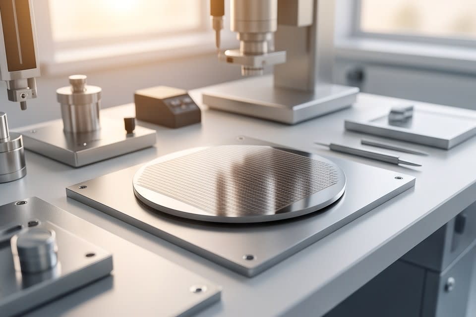
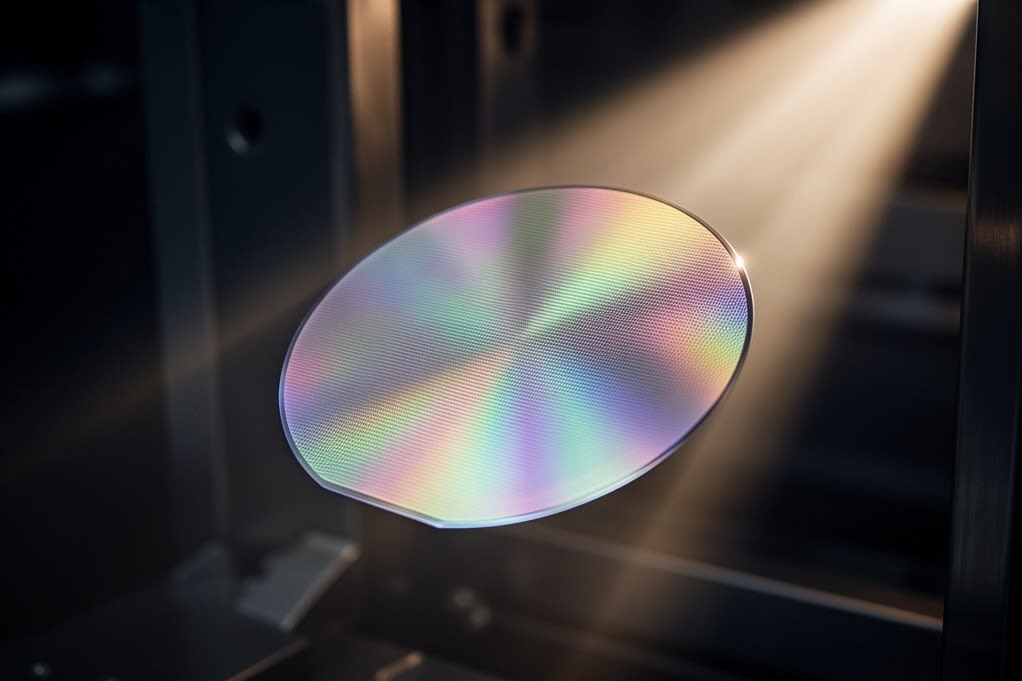
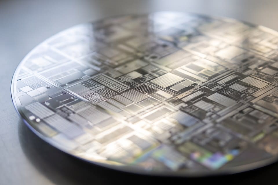
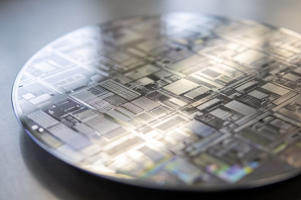
    Semiconductor wafer densely patterned with microscopic circuit lines

    As the linewidths of circuits etched onto a single semiconductor chip have narrowed to the scale of just a few nanometers, the limits of acceptable contamination in the manufacturing process have also changed. In the past, it was enough to filter out foreign matter that was difficult to detect with the naked eye. Today, even a single fine particle floating in the air can become a variable that damages an entire circuit. As processes become more precise, the standards required of cleaning equipment have risen as well, and cleaning has become a core process that determines yield, not a final step for checking quality.
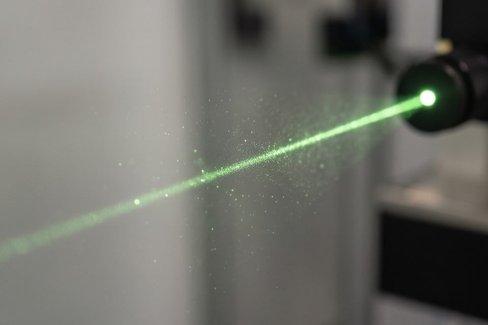
    Airborne fine particles visualized and floating in laser light

    The structure in which particle contamination determines yield

    In semiconductor processes, the impact of particle contamination on yield increases sharply as process generations advance. According to Applied Physics USA, in sub-10nm processes, aerosols measuring 0.1 to 0.5 micrometers are considered among the greatest risk factors, and even a single 10nm particle can cause a short circuit or structural deformation in a transistor.

    The reality that even within the same production line, yield can vary between 95% and 75% depending on the level of particle contamination control shows that the cleaning process is not simply a matter of hygiene. As miniaturization progresses, the tolerance for contamination becomes narrower, and how precisely foreign matter is removed in the early stages of the process effectively determines the quality of the final product. This is why cleaning equipment is no longer a lower priority in process design, but has moved to the center of yield strategy.

    As particle size becomes smaller, the precision required to detect and remove those particles also increases. Process miniaturization is changing the very criteria used to select equipment.

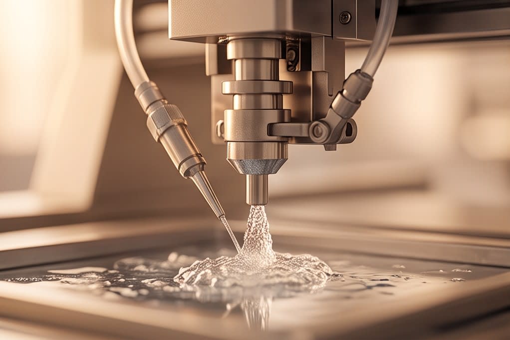
    Dynamic bubbles formed as water droplets fall

    Principles and field application of multi stage cleaning technology

    The performance of cleaning equipment depends on how contamination particles are separated from the surface. Micro bubble cleaning removes particles with shock waves generated when bubbles tens of micrometers in size collapse near the surface. In a study published in the Korean Journal of Chemical Engineering, a maximum jet flow velocity of 148.5mm/s was confirmed in a micro cylinder array structure, and this level of flow velocity is effective for removing fine contaminants with strong surface adhesion.

    Nanobubble technology uses bubbles smaller than 5nm to reach even finer particles, and because the bubbles remain stable for a long time, cleaning efficiency is maintained even on complex surface structures.

    Engineers handling components with different shapes in the field, such as camera modules, sensors, VCM motors, and trays, understand that it is difficult to process every product with a single method. This is why multi stage cleaning structures that combine Micro Bubble, Water Jet, and Air Knife are chosen for actual production lines.

    The drying process, which completely removes residual moisture after cleaning, must also be integrated into a single flow to reduce the risk of foreign matter reattaching between processes. Designing cleaning and drying as one continuous system has become essential for securing quality stability.
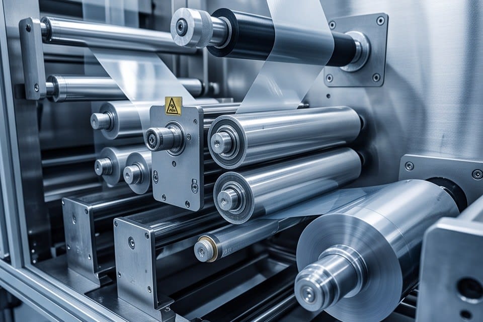
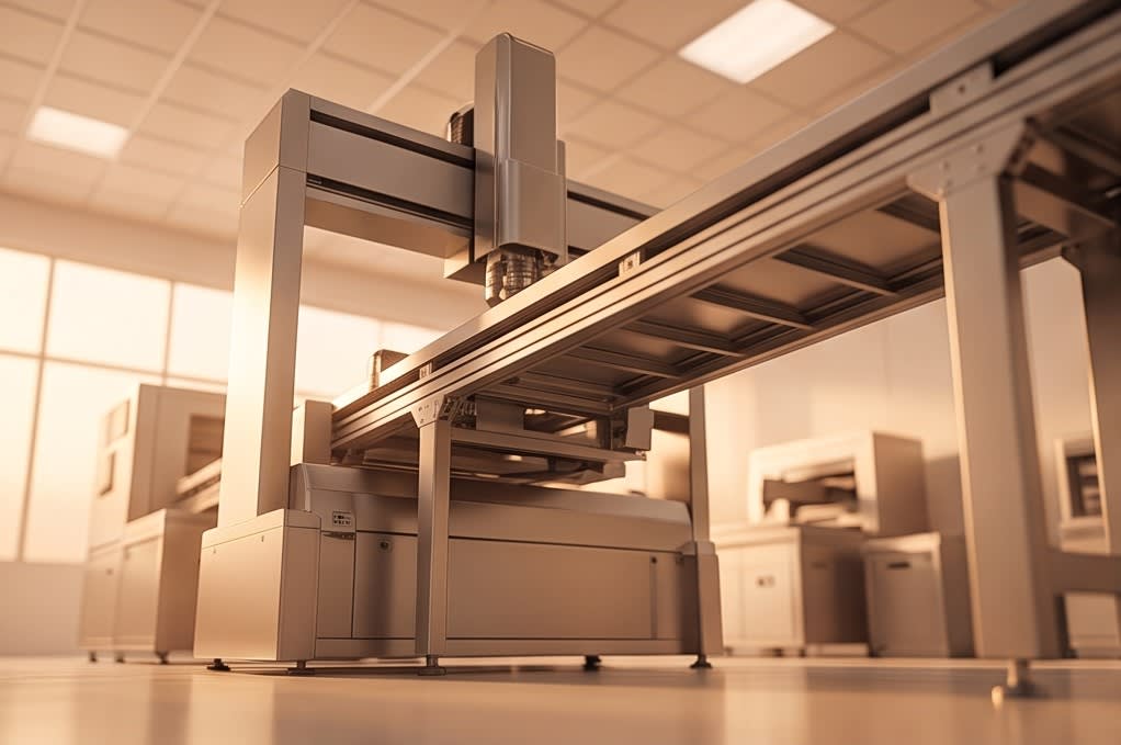
    Drive unit of lamination equipment where tape is supplied through rollers

    Thickness uniformity and process integration determine defect rates

    To reduce defects in the package processing stage, the first requirement is to clearly define the criteria for selecting equipment. The allowable range of total thickness variation, TTV, required in high performance packaging is typically 0.5 to 2.0 micrometers, and this standard becomes even stricter for products that stack chips in multiple layers, such as AI semiconductors and high performance memory.

    Huvics takes an approach that structurally reduces defect factors occurring after cleaning through its PKG Grinder and Laminator System. The PKG Grinder uses a high precision stage and diamond wheel to uniformly process various packages, including FCBGA, WLCSP, QFN, and DFN, at the micron level, and its core role is to keep thickness variation within the allowable range. The Laminator System handles tape attachment and curing processes from Expander to UV Curing within a single line, reducing contamination and alignment errors that can occur during movement between processes.

    Cases in which defects in semiconductor tape bonding processes or foreign matter issues in camera modules were resolved through cleaning and integrated process design show that equipment selection goes beyond simply comparing specifications. As stacking becomes deeper and package structures become more complex, thickness uniformity and process continuity act as the criteria that determine defect rates. The answer to what it means for final yield to reduce variables at a specific process stage is already embedded in the equipment design.
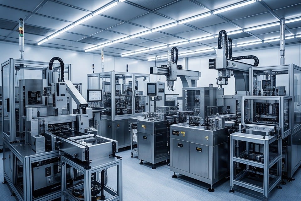
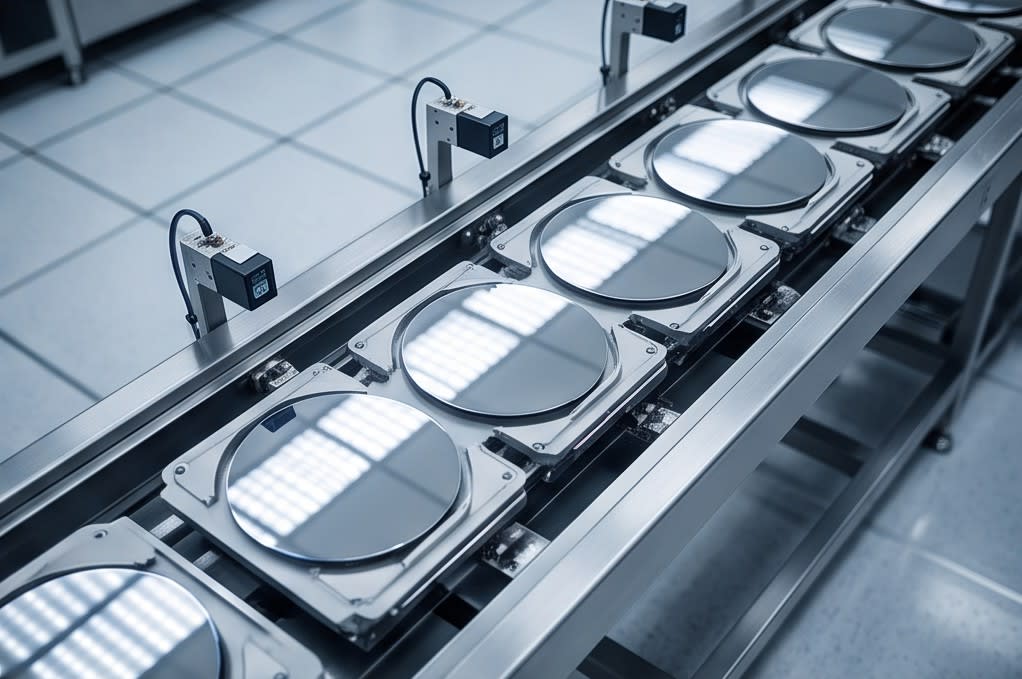
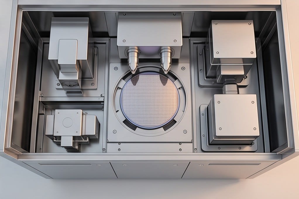
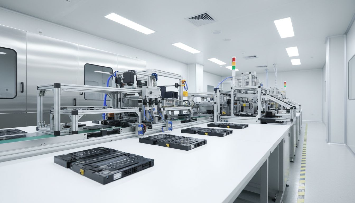
    Precision automation equipment organically arranged at a semiconductor production site

    As semiconductor processes become more precise, the role of cleaning and processing equipment is shifting from simple support to the center of yield management. In an environment where the size of a single contamination particle can affect overall yield, the principle used to remove particles and the method used to control thickness variation become the practical standards for equipment selection. As the pace of process miniaturization accelerates, the importance of equipment that meets these standards will continue to grow.


    Huvics is an advanced technology company that develops and manufactures automation equipment and
    production systems across the semiconductor, LED, Mobile, and Cosmetic industries.
    With top talent and continuous technological innovation, Huvics supports customers in improving productivity and
    securing quality competitiveness.

    Huvics Contact

    Phone: 031-374-8285
    Email: cdpark@huvics.com

    Huvics Inquiry

  • How to Manage Grinding, Lamination, and UV Curing Stages to Improve Chip Stacking Yield

    How to Manage Grinding, Lamination, and UV Curing Stages to Improve Chip Stacking Yield

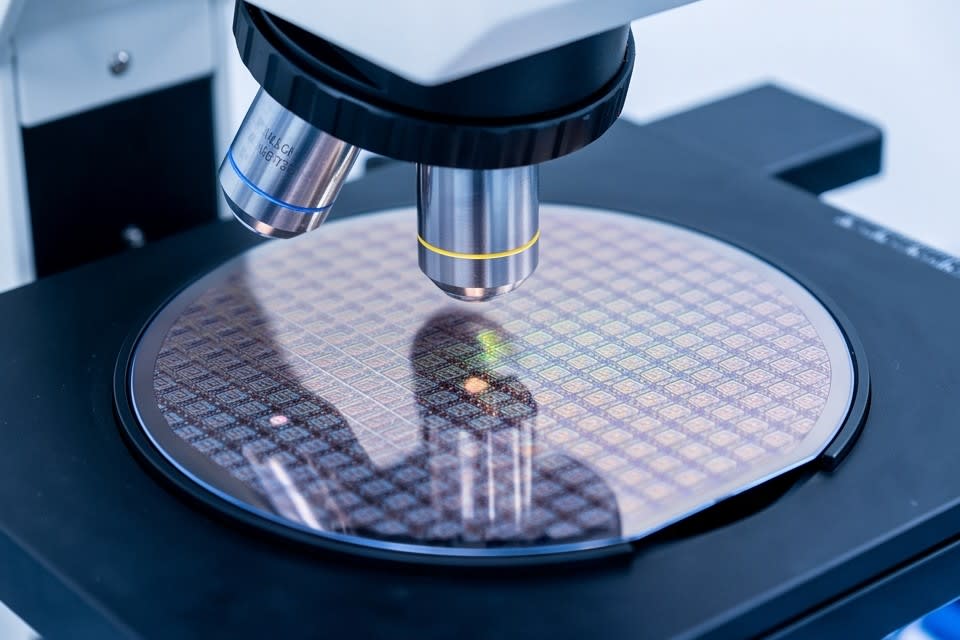
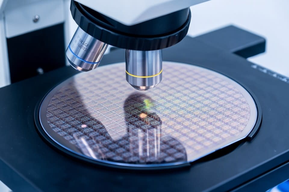
    A detailed inspection of a semiconductor wafer surface using optical equipment

    If you are an engineer designing semiconductor packages, you have probably encountered this situation at least once. Even after carefully setting the process conditions, step differences appear between chips after stacking, and yield data begins to fall below expectations. When tracing the root cause, the issue often comes down to thickness variation and flatness control. Even though this pain point is well known, the same trial and error is often repeated on production sites.

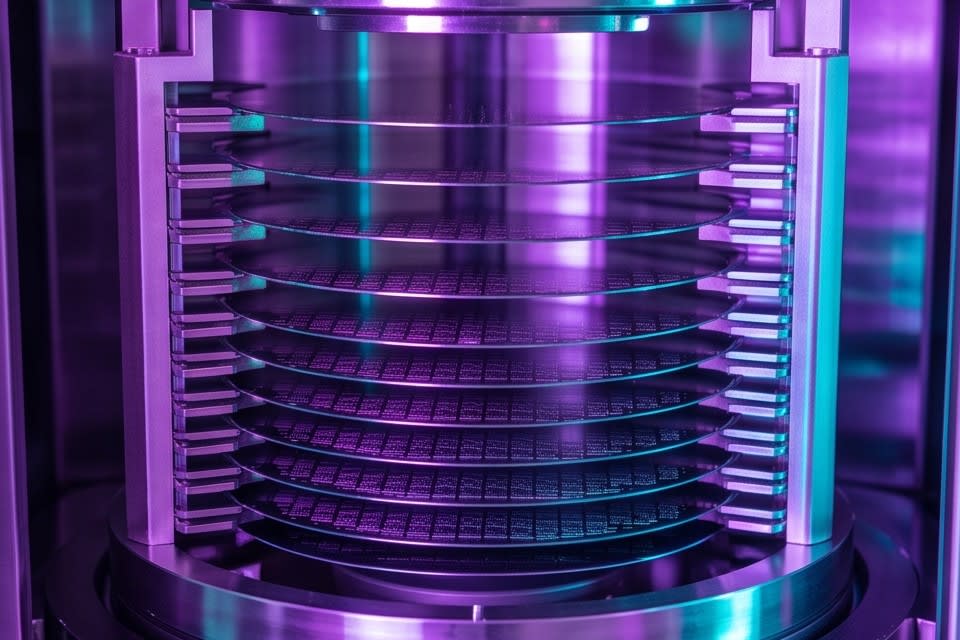
    Multiple wafers vertically aligned and stacked

    Why the shift to stacked structures made thickness control a prerequisite for the process

    As semiconductor package structures have shifted from single layer designs to stacked architectures, the thickness and flatness of each individual chip now require a level of precision that cannot be compared with the past. In single layer structures, a certain degree of thickness variation in individual chips could be tolerated, but in 3D stacked structures where multiple chips are stacked vertically, errors in each layer accumulate, meaning even one uneven chip can compromise the reliability of the entire package.

    In fact, research published on NCBI/PMC confirms that in advanced 3D stacking processes, chip thickness is reduced from around 780μm to 10μm or less, while total thickness variation TTV must be controlled to 1μm or below. As chips become thinner, the signal travel distance decreases, improving power efficiency, while lower thermal resistance also enhances heat dissipation performance.

    In this way, thinning is directly linked to performance improvement, but it also raises the difficulty of maintaining thickness uniformity. Micron level variation can change mechanical stress at the bonding interface after stacking and may ultimately lead to failures in long term reliability testing. As packaging technology advances, thickness control is becoming not an option, but a prerequisite for the process.

    Precision processing of a wafer surface using grinding equipment fitted with a diamond wheel

    How the precision of grinding equipment determines thickness uniformity

    To secure thickness uniformity in an actual process, the precision of the grinding equipment becomes a key variable. A grinding method that combines a high precision stage with a diamond wheel can uniformly process wafer or package surfaces down to the micron level, enabling stable achievement of target thickness across various package types such as FCBGA·WLCSP·QFN/DFN.

    What matters is whether the equipment not only grinds thinner, but also has the control capability to minimize variation throughout the grinding process. The Huvics PKG Grinder is high precision grinding equipment designed based on this principle, supporting both Full Auto and Manual Type configurations so it can be flexibly applied according to the production line scale and automation level of customers.

    The ability to maintain quality stability even under high speed process conditions and achieve high yield is an especially important criterion in mass production environments. Consistent processing capability that stays within allowable tolerances regardless of package type is the first standard to examine when selecting grinding equipment for a stacked package process.

    Equipment performing UV curing on dicing tape for adhesion control and chip separation

    How lamination and UV curing connect grinding precision to yield

    If the grinding process plays the role of precisely removing thickness, then how safely chips are fixed and separated in the preceding and following stages also determines the yield of the overall process. In the tape mounting process using dicing tape, if adhesion is too strong, surface damage can occur when separating chips. Conversely, if adhesion is insufficient, chips can shift during processing and increase thickness variation.

    The key method for achieving this balance is UV curing. UV curable dicing tape weakens under controlled adhesion conditions after UV irradiation, allowing chips to be separated without damage. Furthermore, when UV curing is applied as a pretreatment before lamination, it can permanently reduce the adhesion of the dicing tape and improve the stability of subsequent processes. In this way, the timing and condition settings of UV curing are not simply an additional process, but a turning point that connects grinding precision to actual yield.

    The Huvics laminator system supports a one stop configuration that handles everything from Expander to UV Curing within a single line, and both Lamp and LED methods can be selected, enabling adhesion strength control tailored to product characteristics and process requirements. By integrating process steps, tact time is reduced, and the risk of contamination or damage that may occur during transfer between stages is also lowered. When grinding and lamination are designed as one continuous flow rather than separate processes, the meaning of securing thickness uniformity is finally completed.

    Semiconductor packages arranged in a tray at uniform intervals and shapes

    In the era of stacked semiconductors, thickness uniformity and flatness are ultimately not issues of just one process step. Only when grinding precision, tape adhesion control, and UV curing timing work together organically can they lead to yield stability. When tracing the causes of repeated step defects and yield loss on production sites, the answer ultimately returns to how precisely these processes are connected.


    Huvics is an advanced technology company that develops and manufactures automation equipment and
    production systems across the semiconductor, LED, Mobile, and Cosmetic industries.
    With top talent and continuous technological innovation, we support customers in improving productivity and
    securing quality competitiveness.

    Huvics Contact

    Phone: 031-374-8285
    Email: cdpark@huvics.com
    Huvics Inquiry

  • Semiconductor Process Defects, Solve Them in 3 Steps: Cleaning, Lamination, and Grinding

    Semiconductor Process Defects, Solve Them in 3 Steps: Cleaning, Lamination, and Grinding

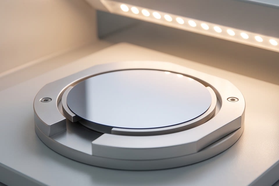
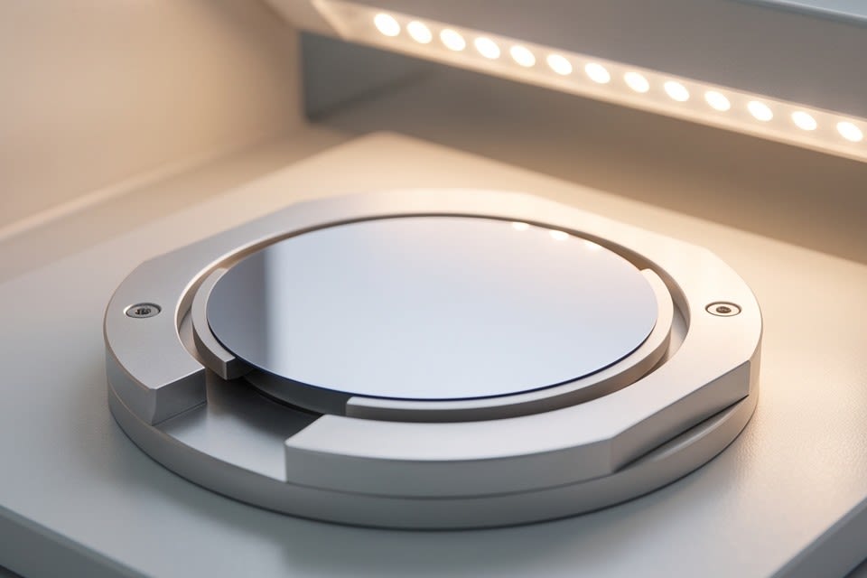
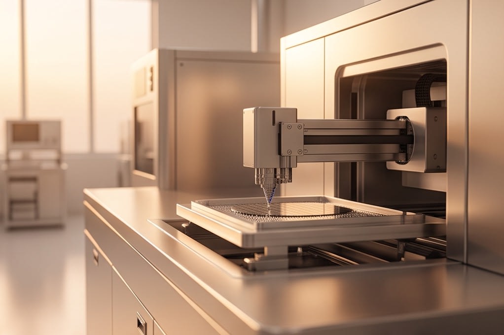
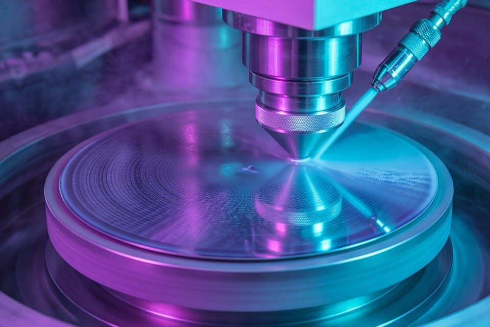
    A semiconductor wafer mounted on a circular stage inside equipment

    Just a few years ago, semiconductor cleaning was considered little more than the ‘finishing step’ of the process. However, as chip integration increases and package structures become more complex, precision processes such as cleaning, lamination, and grinding are emerging as key variables that determine final yield. In semiconductor manufacturing sites, the required precision level for these processes will continue to rise.

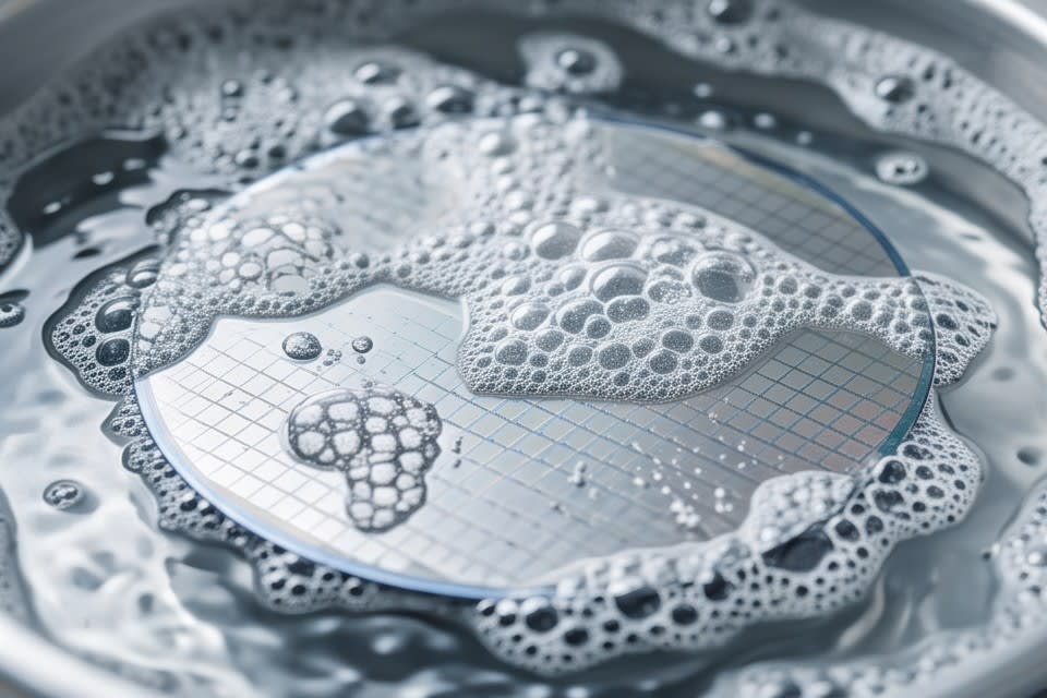
    Bubbles forming on the surface of a semiconductor wafer

    Why the Cleaning Process Is the Starting Point of Yield

    In semiconductor production lines, the seeds of defects grow where they cannot be seen. A single microscopic contaminant particle remaining on the surface of a wafer or tray can disrupt the yield of the entire subsequent process. This is exactly why cleaning is not simply ‘washing away’.

    The micro nanobubble method, which generates fine bubbles of 0.1μm or smaller in water to remove organic matter, effectively separates contaminants while minimizing physical impact on the surface. The principle is that the localized pressure generated when bubbles collapse detaches particles from the surface. When a multi step configuration is added, using Water Jet to push away foreign matter and Air Knife to remove moisture, cleaning efficiency becomes significantly different compared to a single method.

    The more contamination sensitive the ultra precision components are, such as camera modules, autonomous driving sensors, and VCM motors, the more clearly the effect of this multi step cleaning appears. The Huvics Cleaner System is equipment configured to apply this multi step cleaning principle to actual mass production environments, and it is equipped with an Oven Dry function to handle the drying process as part of a single flow. This structure reduces the risk of recontamination that can occur when cleaning and drying are separated. Ultimately, the understanding is taking hold in manufacturing sites that cleaning is the starting point of the process and the foundation for quality in all later stages.

    Tape being attached to the surface of a semiconductor wafer

    Why Precise Control in the Lamination Process Matters

    One of the defects that occurs most quietly yet critically in the lamination process is adhesive residue. UV curing tape operates on the principle that its adhesive strength decreases when exposed to ultraviolet light, making it easier to separate chips from the tape after dicing. The problem occurs when sufficient UV energy is not delivered. If curing is incomplete, adhesive remains on the chip surface, and this residue can become a contamination source in subsequent processes or affect electrical characteristics.

    On the other hand, excessive UV exposure can cause thermal damage to the tape substrate or the chip itself, making the precision of energy control a key variable that determines process results. The same applies to adhesion uniformity in the Tape Mounting step. If the tape is not evenly attached, the chip can move slightly during dicing, reducing cutting precision.

    The Huvics Laminator System processes the steps from Expander to Tape Mounting and UV Curing within a single system, and it is configured to selectively apply two UV methods: Lamp and LED. By integrating process steps, the key is to reduce condition fluctuations that can occur between each step and to maintain stable adhesive strength and curing quality.

    A patterned silicon wafer placed on precision equipment

    In the Era of Stacked Packages, Grinding Precision Determines Performance

    As stacked package technology, which stacks chips in multiple layers, becomes more advanced, requirements for thickness uniformity and surface flatness in each layer become stricter. Traditional bump based stacking structures created a gap of about 30μm between dies, but hybrid bonding, which directly connects copper to copper, reduces this gap to nearly 0. As the gap narrows, the allowable range of thickness variation in the grinding process also narrows.

    In products that stack dozens of chips, such as AI semiconductors or high performance memory, accumulated thickness variation in one layer can collapse the flatness of the entire package, leading to electrical connection defects. The Huvics PKG Grinder is equipment that uses Diamond Wheel based micron level grinding to uniformly process packages to the thickness required by customers across various package types such as FCBGA, WLCSP, and QFN/DFN. It supports both Full Auto and Manual configurations, securing flexibility for production lines. As stacked structures become denser and packages become thinner, it will become even clearer in future technology competition that grinding precision is a condition that determines the performance and reliability of next generation semiconductors.

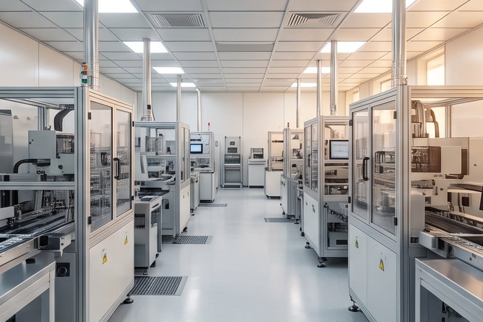
    A semiconductor manufacturing production line with various automated equipment arranged in alignment

    Cleaning, lamination, and grinding may appear to be independent processes, but these three steps are connected as one quality chain. Contamination in an earlier step disrupts precision in a later step, and subtle differences in curing conditions determine the reliability of the final chip. Preventing defects in semiconductor processes ultimately comes down to how tightly these invisible connections are managed.


    Huvics is an advanced technology company that develops and manufactures automated equipment and
    production systems across the semiconductor, LED, Mobile, and Cosmetic industries.
    With top talent and continuous technological innovation, we support improved customer productivity and
    secure quality competitiveness.

    Huvics Contact

    Phone: 031-374-8285
    Email: cdpark@huvics.com

    Huvics Inquiry

  • Precision Cleaning and Process Automation Solutions That Determine Semiconductor Wafer Yield: Analysis of Huvics Technology

    Precision Cleaning and Process Automation Solutions That Determine Semiconductor Wafer Yield: Analysis of Huvics Technology

    Huvics

    In semiconductor manufacturing, even a microscopic residue invisible to the eye can become the trigger for a major defect. Today, as nanoscale precision processes have become standard, the cleanliness of the wafer surface is more than just one step in the process. It is a key indicator that determines the final product yield. Because such micro contamination directly leads to significant cost losses for companies, thorough and flawless surface management has now become a strategic necessity rather than an option.

    Based in Osan, Gyeonggi-do, Huvics is a group of specialists that has transformed deep challenges from the field into technical solutions, from semiconductor tape bonding processes to tray cleaning technology. Let us take a closer look at the core of the innovative process design Huvics offers for your journey to maximize production yield through precision cleaning and process automation.

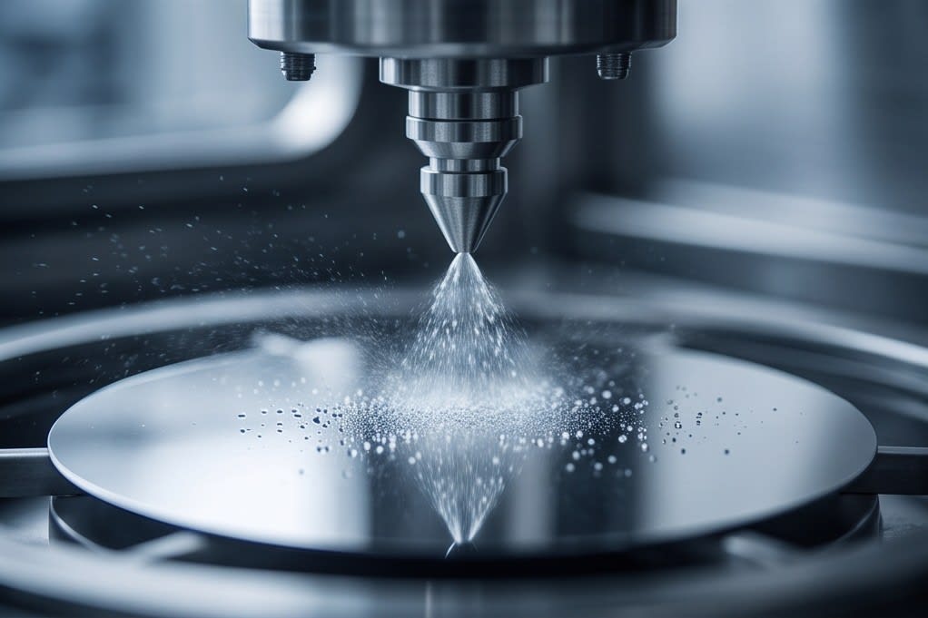
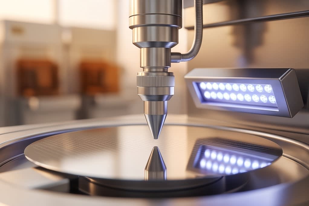
    Cleaning technology with an ultra-precision nozzle

    The Core of Semiconductor Processes, Precision Cleaning Technology

    The Impact of Micro Contamination on Yield

    In semiconductor manufacturing processes, the cleanliness of the wafer surface is a key indicator that determines the final product yield. In the modern semiconductor ecosystem, where nanoscale micro processes have become routine, even a tiny residue invisible to the eye can disrupt the pattern of fine circuits and become a critical variable that produces defective products in large quantities. Defects caused by this micro contamination directly lead to enormous cost losses for companies and ultimately weaken price competitiveness in the market.

    Huvics’ Technical Solution

    Huvics deeply understands these on-site concerns and provides the following technical solutions.

    • Solving challenging defect issues in semiconductor tape bonding processes
    • Overcoming technical difficulties encountered in tray cleaning processes
    • Responding based on extensive hands-on experience accumulated in the field

    We go beyond simply providing cleaning and support automation and simplification design across the entire manufacturing process of our customers. Through this, companies can significantly reduce unnecessary operating costs while maximizing consistency and stability in process quality. Precision cleaning technology ultimately lowers defect rates, optimizes equipment uptime, and improves overall productivity.

    With Huvics, which continues to build unmatched technological capabilities in precision cleaning and automation equipment through constant research and development, experience the highest production yield your semiconductor process can achieve.

    Site-Customized Process Redesign

    Solving Technical Challenges and Optimizing Processes

    The solutions provided by Huvics go beyond the step of simply removing contamination. They focus on fundamentally solving technical challenges in manufacturing sites and redesigning process workflows. In particular, Huvics presents site-customized response strategies by dramatically improving micro defect issues in the tape bonding process, a chronic problem in the semiconductor industry, and overcoming the physical limitations of tray cleaning technology. The many variables encountered in the field are difficult to solve with a fragmented approach.

    Sustainable Innovation and Automation Integration

    Based on years of accumulated field data, Huvics builds the most efficient precision cleaning process and tightly integrates it with automation systems. By introducing precise process automation and process simplification, we reduce the burden of chronic operating costs faced by companies while also practicing sustainable innovation that maximizes process quality stability.

    Our proven technological capabilities, developed through close collaboration with leading global companies, have become the most powerful core driver for increasing production yield in increasingly sophisticated micro process environments. When the invisible obstacles that hinder process efficiency are removed one by one through the professional perspective of Huvics, your manufacturing competitiveness will finally reach results with a higher level of perfection.

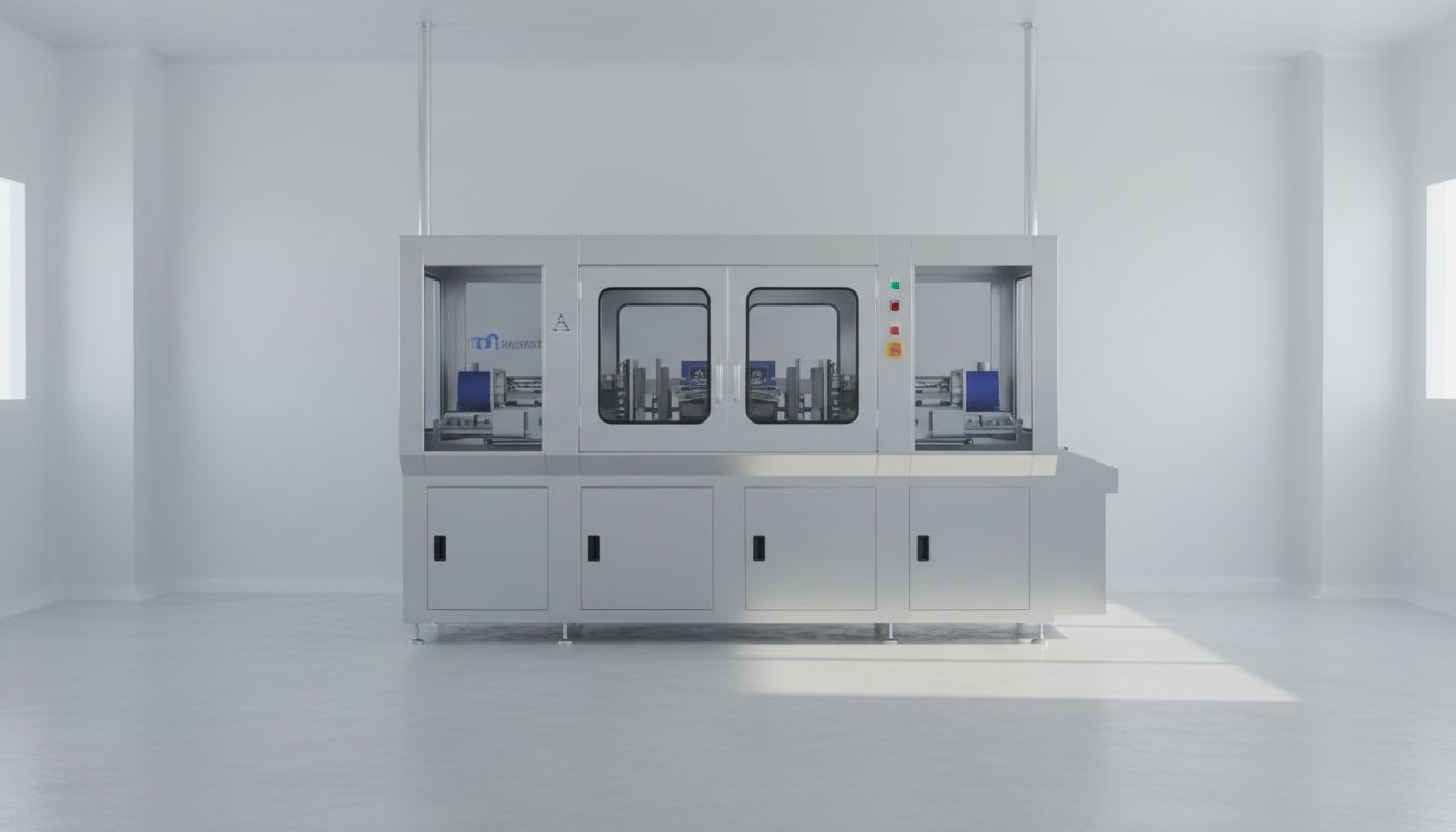
    Overview of automated equipment inside a cleanroom

    System-Based Automation Solutions

    Automation Systems for Quality Assurance

    Productivity in semiconductor manufacturing ultimately depends on how effectively invisible contamination is controlled. However, as processes become more complex, there are limits to direct human management. Huvics is advancing system-based automation solutions to address these limitations. Precision cleaning equipment is not simply a machine that wipes products clean. It is a quality assurance system that helps maintain consistent cleanliness from the beginning to the end of the process. Huvics technology, which blocks difficult contamination factors such as tape residue and fine particles at the source, is installed at key points across semiconductor production lines to continuously monitor potential threats.

    Improving Productivity and Preventing Human Error

    Reducing defect rates in the field is not simply about preventing losses. It is about increasing the mass production share of high-value-added products. Huvics diagnoses inefficient manual processes that customers struggle with and replaces them with the latest automation equipment, minimizing the room for human intervention. This improves the work environment, prevents human error, and dramatically enhances process efficiency. Huvics solutions, which integrate technical know-how accumulated in the field, solve the practical challenges customers face and help them secure manufacturing competitiveness at the next higher level.

    Efficient wafer process flow

    Huvics Technology Portfolio and Future Value

    Business Success Through Customized System Implementation

    The broad technology portfolio held by Huvics is the most powerful tool for actively responding to the demanding requirements of the rapidly changing semiconductor market. Based in Osan, Gyeonggi-do, we continue to invest in research and development while advancing our technological capabilities in precision cleaning and automation equipment. On this foundation, we accurately diagnose inefficiencies in the complex manufacturing processes faced by customers and build customized systems that boldly reduce unnecessary steps, thereby substantially driving the business success of our partners. Maintaining stable quality standards amid a rapidly changing market environment is more important than anything else, and Huvics aims to be your trusted supporter at the center of creating those standards.

    Partnership for Process Innovation

    Beyond simply improving existing problems, an innovative approach that changes the paradigm of the process presents higher quality standards in the next generation semiconductor industry while also becoming a solid foundation for sustainable growth. Accumulated technological expertise in precision cleaning and deep understanding of field automation are the distinctive competitiveness of Huvics. We will provide full technical support so that your company can go beyond simple cleaning, enhance the perfection of the entire process, and achieve overwhelming production yield in the market. Through the precise technology and sincere partnership of Huvics, complete your process innovation and create future value together through higher production yield.

    Final quality of a defect-free wafer

    In semiconductor manufacturing, invisible micro contamination becomes a decisive variable that determines corporate competitiveness. Because cleanliness that may seem minor creates the major result known as yield, process perfection is now completed through collaboration with a partner that has technical insight.

    Based on precision cleaning technology and process automation solutions that fundamentally solve complex on-site challenges, Huvics will help your company surpass the limits of production yield and take the lead in the market. Removing invisible obstacles and innovating the process paradigm. Now, add overwhelming growth momentum to your business through the professional perspective of Huvics.


    Huvics is an advanced technology company that develops and manufactures automation equipment and
    production systems across the semiconductor, LED, Mobile, and Cosmetic industries.
    With top talent and continuous technological innovation, we support customers in improving productivity and
    securing quality competitiveness.

    Huvics Contact Information

    Phone: 031-374-8285
    Email: cdpark@huvics.com

    Contact Huvics

  • The Value of Precision Cleaning in Semiconductor Yield and the Process Innovation Strategy of the Huvics One Stop Laminator

    The Value of Precision Cleaning in Semiconductor Yield and the Process Innovation Strategy of the Huvics One Stop Laminator

    Huvics

    An industry saying states that the success or failure of semiconductor manufacturing is determined not at the beginning of a massive process, but by the level of cleanliness at the final stage. Today, that message carries even greater weight. At a time when even invisible microscopic contamination can undermine the reliability of an entire product, precision cleaning has become the final safeguard that determines production yield, going far beyond a simple auxiliary measure.

    To block unnecessary exposure within complex assembly lines and reach the highest level of manufacturing efficiency, we will explore how the process integration strategy presented by the Huvics one stop laminator system can resolve chronic bottlenecks in semiconductor manufacturing sites and maximize competitiveness.

    Integrated Laminator Solution by Huvics

    The Importance of Precision Cleaning in Determining Semiconductor Yield

    Core Value in Back End Processes

    The semiconductor manufacturing process is often described as a continuous series of fine processes, but in reality, the back end stage at the peak of that process is the most sensitive section that determines yield. Just before a wafer fully takes shape as a chip, the introduction of even a single microscopic contaminant can cause critical damage to the reliability of the entire product.

    For this reason, today precision cleaning systems have become a core process that fundamentally blocks defect factors and guarantees final product quality, rather than merely serving as an auxiliary method for removing foreign substances. In increasingly complex and sophisticated semiconductor structures, it is no exaggeration to say that cleanliness in the final stage is the last line of defense for measuring product completeness.

    Strengthening Production Efficiency and Competitiveness

    In particular, at sites where advanced equipment such as the Huvics one stop laminator is introduced, precision cleaning acts as a solution that removes chronic bottlenecks in the manufacturing process. This process goes beyond maintaining cleanliness and becomes a pivotal point that makes the entire production line flow more flexibly and dramatically improves final yield.

    Only chips completed in the cleanest possible state can meet the strict requirements of the market, and this precision cleaning strategy becomes the most reliable foundation for maintaining manufacturing competitiveness in the rapidly changing global semiconductor market.

    Core of Precision Cleaning and Curing Processes

    Technological Innovation of the Huvics One Stop Laminator

    Perfect Control of Potential Risk Factors

    The reason the Huvics precision cleaning system receives outstanding evaluations in the field is that it goes beyond the technical level of removing visible foreign substances. Inside the manufacturing environment, microscopic defect factors that are difficult to detect with the naked eye are constantly present, and the Huvics system detects these potential risk factors in advance and prevents them before they occur, ensuring product quality uniformity at a level close to perfection.

    The core technologies implemented by Huvics in the latest semiconductor assembly lines are as follows.

    • Improving process efficiency by applying an LED based UV curing process
    • Operating the precision cleaning process and UV curing stage in an organically integrated manner

    Process Efficiency Through Integrated Equipment

    In the past, each process was separated, resulting in frequent product movement, and the gaps and unnecessary exposure generated during that movement often caused takt time delays and potential contamination. However, Huvics has overcome these physical limitations by processing everything from tape mounting to expander operation and precise UV curing within a single piece of equipment.

    This integrated method, which controls residues in real time and achieves optimal adhesion strength, strengthens product durability while minimizing unnecessary movement, thereby maximizing process stability. From the producer perspective, it provides a powerful tool to minimize the probability of defects even within complex assembly stages, which directly leads to a dramatic improvement in overall production efficiency.

    Huvics is proving directly in the field that precision cleaning is a core strategic asset that supports the stability of the entire manufacturing process, going beyond simple cleanliness maintenance.

    Precise Design of the Huvics System

    A Strategic Choice for Manufacturing Innovation

    Ultimately, the competitiveness of semiconductor manufacturing depends not on the act of cleaning chips itself, but on how perfectly invisible uncertainty can be controlled. True manufacturing innovation begins only when precision cleaning is redefined from a simple maintenance concept into a strategic asset that integrates the process flow and secures quality uniformity.

    As proven by the integrated equipment of Huvics, the choice to transform process complexity into efficient simplicity will become the most powerful weapon for protecting irreplaceable quality value in a rapidly changing market. Now is the time to remove the invisible contamination factors hidden in your production line and experience a higher level of yield completeness.


    Huvics is an advanced technology company that develops and manufactures automation equipment and
    production systems across the semiconductor, LED, Mobile, and Cosmetic industries.
    With top talent and continuous technological innovation, we support customers in improving productivity and
    securing quality competitiveness.

    Huvics Contact Information

    Phone: 031-374-8285
    Email: cdpark@huvics.com

    Huvics Inquiry

  • Huvics 4-Step Cleaning and Drying System—Core Technology for Achieving Unmatched Quality in IT Components

    Huvics 4-Step Cleaning and Drying System—Core Technology for Achieving Unmatched Quality in IT Components

    Huvics

    As the performance of today’s IT devices continues to advance, the key factor that determines product completeness depends on how perfectly even the finest contamination is managed. In demanding manufacturing sites where even invisible particles are not tolerated, Huvics sets a new standard for quality based on its unrivaled technological expertise.

    Core Technologies of the 4-Step Cleaning and Drying System

    Huvics’ 4-Step Cleaning and Drying System provides a precision solution that completely removes microscopic contaminants from the surfaces of advanced components. The main technologies of this system are as follows.

    • Removal of fine contaminants using microbubbles
    • Powerful cleaning through water jet technology
    • Surface residue removal with air knife technology
    • Residual moisture treatment through oven drying functionality

    Going beyond simple cleaning, the system uses its built-in oven drying function to thoroughly remove residual moisture, implementing an integrated batch process that combines cleaning and drying into one workflow. This unique Huvics system is recognized as essential equipment in automotive electronics manufacturing sites that demand the highest level of quality stability, such as camera modules and autonomous driving sensors.

    Ultimately, Huvics’ process technology, which leaves no fine contamination unchecked, minimizes product defect rates and maximizes reliability, making it a solid starting point for creating the unmatched quality pursued across the IT industry.

    Precision process in an advanced manufacturing site

    Residual Moisture Control and Process Stability

    In particular, the high-performance oven drying technology built into the Huvics system perfectly controls residual moisture that may occur immediately after cleaning and supports a batch processing method that completes the drying process in a single step. If even a small amount of moisture remains on a component during manufacturing, it can later become a critical cause of corrosion or performance degradation. Huvics fundamentally blocks this risk and maximizes process stability.

    This integrated solution dramatically improves production efficiency at manufacturing sites while proactively eliminating unexpected defect factors, making the overall process flow smoother and more stable. In advanced manufacturing environments that require high-level technology, even the smallest difference creates a quality gap. Introducing the integrated Huvics process system means going beyond the installation of excellent cleaning equipment and securing strong competitiveness that can maintain consistent high quality in any environment.

    Automated batch production process

    The Ideal Partner for the Automotive Electronics Industry

    Today’s automotive electronics industry, centered on camera modules and autonomous driving sensors, demands strict quality standards that do not allow even the slightest error. In such a harsh and precise environment, enabling components to fully deliver their intended performance ultimately depends on how thoroughly the cleaning process is managed.

    Huvics’ cleaning solution proves outstanding stability at this critical point and is recognized as the ideal partner for ensuring component quality under even the most demanding process conditions. In the highly technical IT component market, even one small contaminant can determine a company’s competitiveness. The unrivaled cleaning technology provided by Huvics goes beyond simply removing contaminants and becomes a reliable technological foundation that helps companies secure an overwhelming advantage in the market.

    Huvics integrated cleaning system

    Huvics as a Technology Partner

    Ultimately, the direction of Huvics is very clear. It is to take responsibility for quality even in unseen areas so that customers can maximize product completeness and earn market trust, thereby realizing true unmatched quality. Competition in the IT industry is intensifying day by day, and producing smaller and more precise components has become a key challenge for every company.

    Within this trend, Huvics goes beyond being a simple equipment supplier and serves as a technology partner that shares manufacturing site challenges and presents solutions. By preventing in advance the potential risks that even a single small particle can create, the Huvics 4-Step Cleaning and Drying System allows companies to enjoy an optimal environment where they can focus more fully on product production.

    The completeness of advanced IT components is ultimately determined by the precision required to control even invisible microscopic contaminants. For every company seeking unmatched quality, Huvics presents the most reliable answer.

    Manufacturing site that improves production efficiency


    Huvics is an advanced technology company that develops and manufactures automation equipment and
    production systems across the semiconductor, LED, Mobile, and Cosmetic industries.
    With top talent and continuous technological innovation, we support customers in improving productivity and
    securing quality competitiveness.

    Huvics Contact Information

    Phone: 031-374-8285
    Email: cdpark@huvics.com

    Huvics Inquiry

  • Huvics 4-Stage Cleaning and Drying System Captures Global Market Attention – A Defect-Free Quality Solution for Semiconductors and Precision Parts

    Huvics 4-Stage Cleaning and Drying System Captures Global Market Attention – A Defect-Free Quality Solution for Semiconductors and Precision Parts

    Huvics

    In semiconductor and ultra-precision parts manufacturing, even a single microscopic contaminant can become a critical variable that determines the success or failure of the entire process. Today, when product perfection directly translates into corporate competitiveness, the global market is focusing on perfect cleaning as the engineering answer to achieving defect-free quality.

    Huvics meets the strict demands of these advanced industries and sets a new standard through its distinctive 4-stage cleaning and drying system, which extends from microbubbles to water jets, air knives, and precision oven drying. Let us take a closer look behind this innovative process and see why manufacturing sites around the world choose Huvics solutions and trust its technological expertise.

    Huvics precision cleaning equipment

    Huvics, an Essential Solution for Advanced Manufacturing Sites

    The Core of the 4-Stage Cleaning and Drying System

    In the semiconductor and precision parts industries, cleanliness goes beyond simply maintaining product appearance and becomes a core factor that determines product viability. In advanced manufacturing environments where one tiny particle or invisible contaminant can affect the defect rate of an entire process, perfect cleaning is directly linked to corporate competitiveness.

    Huvics deeply understands these industrial demands and has built the following distinctive 4-stage cleaning and drying system.

    • Separation of microscopic contaminants using microbubbles
    • Powerful removal of foreign matter through water jets
    • Precision surface treatment with air knife technology
    • Removal of residual moisture through precision oven drying

    By perfectly separating and removing even invisible microscopic contaminants, this system has earned strong trust across the industry.

    Huvics cleaning system structure

    Blocking Residual Moisture and Ensuring Quality Stability

    The Huvics approach does not stop at simply wiping away foreign matter. Through the precision oven drying function built into the system, residual moisture immediately after cleaning is dried at once, securing a technological advantage that fundamentally blocks corrosion and quality degradation factors that may be caused by moisture.

    This consistent process treatment prevents unexpected quality defects that may occur during subsequent processes and greatly contributes to productivity improvement at manufacturing sites. If defect-free quality is the most important value in the semiconductor and ultra-precision parts fields today, Huvics presents the most reliable engineering answer for achieving that defect-free quality.

    advanced robotic cleaning process

    Technology Trusted by the Global Market

    Strict Quality Standards and Field Suitability

    The reason Huvics is recognized in the global market for its unmatched technological capability is that it has consistently met the extremely strict quality standards required by the electronics industry. Especially in advanced fields such as autonomous driving sensors and camera modules, where even the smallest error cannot be tolerated, a minor product defect can lead directly to a critical safety issue.

    Huvics cleaning solutions have become core infrastructure that guarantees both efficiency and product stability in processes requiring this extreme level of precision. Field engineers trust the Huvics system for the following reasons.

    • Consideration of harsh field environments from the design stage
    • Consistent cleaning performance maintained even after long operation
    • Technological capability that enables process standardization

    Ultimately, defect-free quality is a non-negotiable standard in the semiconductor and ultra-precision parts industries, and the Huvics 4-stage cleaning and drying system is the most engineering-based and reliable answer for achieving that strict standard. Just as true trust is built when technology proves strong results in real field environments, Huvics will continue to serve as a reliable partner that drives customer success and presents a new standard for advanced industries.


    Huvics is an advanced technology company that develops and manufactures automation equipment and
    production systems across the semiconductor, LED, Mobile, and Cosmetic industries.
    With top talent and continuous technological innovation, we support customers in improving productivity and
    securing quality competitiveness.

    Huvics Contact

    Phone: 031-374-8285
    Email: cdpark@huvics.com
    Huvics inquiry

  • Huvics 4-Step Precision Process that Maximizes Process Efficiency: Site-Specific Solution Strategy

    Huvics 4-Step Precision Process that Maximizes Process Efficiency: Site-Specific Solution Strategy

    Huvics

    In the fierce competition of semiconductor manufacturing sites, you know better than anyone that even a 1 percent difference in yield can determine the success or failure of a company. In particular, subtle defects in the tape adhesion process or recurring tray cleaning issues often remain unresolved challenges for site managers. Can we truly control these invisible variables completely and free ourselves from the technical hurdles we face every day? Huvics goes beyond simply supplying equipment, thoroughly analyzing the unique physical environment of each site and presenting precise answers that maximize process potential. From here, let us explore those answers through the unique 4-step precision process from Huvics, which transforms site complexity into exceptional efficiency.

    Initial diagnosis process of Huvics

    Stage 1: Site-Specific Initial Diagnosis

    Analysis of Process Variables and Root Causes

    Semiconductor manufacturing sites are a world of precision where not even the slightest error is allowed. In particular, subtle defects that occur in the tape adhesion process or the challenges of repetitive tray cleaning are often considered major technical bottlenecks that hinder production efficiency. Huvics does not try to solve these site concerns merely by supplying standardized equipment.

    We focus on the fact that every customer manufacturing line has different physical characteristics and environments. Therefore, from the initial diagnosis stage, we thoroughly analyze invisible variables within the process and the root causes of problems. This precise diagnosis becomes the logical foundation that allows the customized solution to be implemented in the most complete way.

    The First Step in a Strategic Partnership

    From precision cleaning systems to advanced automation equipment, every process designed by Huvics is the first step in a strategic partnership that helps customer production lines achieve the highest efficiency. The initial diagnosis we perform goes beyond simply identifying problems. It is like fastening the first button to bring out the full potential of the process.

    Precision cleaning solution technology

    Stage 2: Differentiated Customized Design and Implementation

    Optimal Engineering Based on Data

    Once the full-scale design stage begins, the differentiated customized engineering of Huvics comes into play. We do not simply place existing equipment on site. Instead, we conduct an optimal design process that closely reflects the extensive site data and unique process characteristics of each customer. This process is a key strategy for directly overcoming the technical challenges within the manufacturing line.

    Productivity Improvement Through Integrated Solutions

    After the design is completed, a 3-step implementation process is carried out to successfully settle precision cleaning systems and automation equipment on site. In this process, the technology of Huvics goes beyond the physical installation of equipment and functions as an integrated solution that designs the organic flow of the entire manufacturing process.

    As a result, these customized integrated solutions minimize unnecessary downtime in manufacturing lines and dramatically improve yield. Through this, companies leading the global IT and automotive electronics industries can secure a solid technical foundation that gives them a commanding advantage in the changing future technology competition environment. Customized design is the surest key to turning site complexity into simplicity.

    Customized design and implementation stage

    Stage 3: Process Stabilization and Real-Time Monitoring

    Continuous Process Tuning and Quality Maintenance

    The final stage after equipment introduction, process stabilization, is the area where Huvics places the greatest focus. No matter how advanced the technology of the equipment is, it is difficult to expect production efficiency if it cannot be fully integrated into the actual manufacturing line. Huvics continuously performs real-time data monitoring and detailed process tuning so that the installed equipment can maintain consistent high quality on site.

    The Role of a Smart Process Partner

    In this process, the equipment goes beyond simple hardware and becomes a smart partner that operates organically within the overall process flow while preventing potential bottlenecks in advance. As a result, this precise stabilization strategy from Huvics becomes a key driving force that helps customers minimize unexpected defects and secure unwavering production competitiveness.

    We make equipment more than machines that simply stand still. We enable it to breathe with the constantly evolving flow of the process. Ultimately, our goal is to become a reliable and sustainable process partner that helps customers maintain the highest productivity in any situation and secure the most dependable technological advantage.

    Precision control and defect minimization

    Stage 4: Future-Oriented Technology Partnership

    Continuous Technical Support and Innovation

    The journey of Huvics does not stop at installing and stabilizing equipment. We provide continuous technical support and future-oriented partnerships so that customer manufacturing lines can maintain optimal performance even in a changing technological environment over time. Manufacturing sites are becoming increasingly advanced, and the challenges that follow are also evolving rapidly.

    The Future of Sustainable Manufacturing

    Huvics anticipates the new technical challenges customers will face and works together to develop strategic solutions that enhance competitiveness across the entire process, beyond the equipment we supply. Through this partnership, customers experience innovation that leads future markets, going beyond the simple introduction of equipment.

    The ultimate goal of Huvics is to become a dependable technology hub that helps customers build a stable production system that remains solid at any technological turning point and become leaders who drive industrial innovation. This 4-step precision process we propose is more than a technology that improves process efficiency. It is a firm commitment to shaping the future of sustainable manufacturing together with our customers.

    Sustainable process partnership

    Conclusion

    The success or failure of semiconductor manufacturing ultimately depends on how precisely invisible errors are controlled. Going beyond simply replacing equipment, the 4-step process from Huvics analyzes complex variables on site one by one and designs an integrated flow. It is the most reliable strategic move a company can make in the ever-changing competition of future technology.

    Just as the precision we pursue becomes a powerful asset that increases customer productivity, Huvics will stay by your side as a partner that overcomes process limitations and realizes unmatched yield. The technical challenge your manufacturing line faces today may very well be the most important turning point for a new leap forward.


    Huvics is an advanced technology company that develops and manufactures automation equipment and
    production systems across the semiconductor, LED, mobile, and cosmetics industries.
    With outstanding talent and continuous technological innovation, we support customer productivity improvement and
    quality competitiveness.

    Huvics Contact Information

    Phone: 031-374-8285
    Email: cdpark@huvics.com
    Huvics Inquiry

  • Why the Early Stage of the Semiconductor Process Matters – Technical Insights and Strategic Value Presented by Huvics

    Why the Early Stage of the Semiconductor Process Matters – Technical Insights and Strategic Value Presented by Huvics

    Huvics

    In semiconductor manufacturing, where ultrafine circuits at the nanometer scale are realized, why do global technology experts point to the very beginning of the process as the most critical battleground above all else? In today’s environment, where even one invisible microscopic particle can disrupt the entire yield, precise cleaning and control in the early stage have become not just a process sequence but a core strategy that determines a company’s survival.

    This is precisely the area Huvics focuses on, having proven its technological reliability in the global market by receiving the USD 1 Million Export Tower award on Trade Day 2025. Let us take a closer look at the decisive insights Huvics has gained in the field, and how the future of semiconductors changes depending on how perfectly the first step of the process is executed.

    View of a semiconductor cleanroom

    The Core of the Semiconductor Process, the Importance of the Early Stage

    The Golden Time That Determines Process Success

    In the vast and complex world of semiconductor manufacturing, why do experts focus so persistently on the beginning, or early stage, of the process? This goes beyond simply being the first step in sequence. It is the decisive golden time that determines the success or failure of the entire production process.

    Today, as semiconductor circuits have become extremely miniaturized to the nanometer scale, even one tiny particle that is difficult to detect under a microscope can shake the reliability of the entire product. How completely and precisely impurities are removed in the early stage of the process directly becomes the most essential indicator that determines final yield.

    Huvics’ Precision Cleaning and Efficiency Maximization

    Huvics deeply understands the importance of this early process and concentrates all its capabilities on strengthening the foundation of the process through precision cleaning technology and advanced automated equipment. Thorough contamination control in the early stage dramatically reduces the complexity of subsequent processes and ultimately creates a powerful virtuous cycle that maximizes the efficiency of the entire production line.

    With years of accumulated proprietary patented technologies and field-centered know-how, Huvics pursues perfection from the very first step of the process as a strategic partner that solves the challenges of semiconductor manufacturing, driving global technological competitiveness.

    Core of precision cleaning technology

    Huvics’ Technology Recognized by the Global Market

    Unique Capabilities and Risk Prevention

    The reason companies like Huvics, which have proven technological reliability, are recognized as key problem solvers in the fiercely competitive global manufacturing field is their unique capability to overcome the high technological barriers present in the early stage of the process. Huvics, which proved its capabilities in the global market by receiving the USD 1 Million Export Tower award on Trade Day 2025, completely blocks potential risks hidden in the early stage of the process in advance, based on numerous patented technologies accumulated over many years and extensive field project experience.

    Value as a Strategic Partner

    This goes beyond the general level of manufacturing support that simply supplies equipment. It carries a highly strategic value by helping customers secure a strong competitive advantage from the starting point of their manufacturing processes. Through continuous research and development investment, Huvics has steadily expanded its portfolio in precision cleaning and automation, and even now works alongside global companies to solve diverse challenges while serving as the most reliable partner in building stable mass production systems.

    Controlling unexpected variables in advance within complex manufacturing processes not only prevents economic losses for companies but also becomes the most reliable line of defense for protecting market share over the long term.

    Advanced automated equipment

    The Technical Standard of the Future Semiconductor Industry

    Securing Market Competitiveness Through Technological Innovation

    The future semiconductor industry will be rapidly reshaped around advanced precision cleaning and automation technologies that go beyond existing limits. Ultimately, the technological gap in the early process will become a key variable that determines a company’s market competitiveness, and this will lead to raising the technical standards of the entire semiconductor ecosystem by one level, beyond simple improvements in manufacturing efficiency.

    Huvics is taking the lead in this change by expanding its portfolio in precision cleaning and automation through continuous research and development investment. We clearly understand that securing the completeness of the early process without any gaps is the most reliable strategy for surviving in the next generation IT manufacturing market and leading innovation.

    Huvics’ Path as a Global Milestone

    With Huvics, which continues to drive the future competitiveness of semiconductors through ongoing technological innovation, customers can design a future one step ahead from the very starting point of the process. Huvics’ steps toward creating global standards based on technological reliability are becoming a new milestone not only for Korea but also for the global semiconductor manufacturing market, and they will remain at the center of continued change.

    Standard of the semiconductor ecosystem

    Expert Recommendations for a Successful Manufacturing Environment

    A Technical Foundation for High-Quality Mass Production

    The reason we must once again recognize the importance of the early stage of the semiconductor process is that the speed of technological progress is incomparably faster than before. As microprocesses become more advanced, the precision of early cleaning serves as a shield that prevents product defects and, at the same time, as an engine that enables high-quality mass production.

    Huvics goes beyond being a company that simply supplies equipment. It pursues value as a group of experts that analyzes process flows, predicts potential errors, and presents optimal solutions. It is an unchanging rule of the industry that the performance of the latest semiconductor devices can be fully realized only on a clean foundation secured in the early process.

    Partnership for Sustainable Growth

    Going forward, Huvics will continue to devote its full efforts to helping customers overcome manufacturing limitations through technology and to providing a successful manufacturing environment where the beginning of the process leads directly to the best results. These continuous efforts will ultimately enhance the brand value of customers and become a key contribution that accelerates the development of the entire semiconductor manufacturing industry.

    The future of semiconductors we envision begins at this very moment, with the commitment to perfecting the very first step of the process.

    Stable mass production system

    Conclusion

    Ultimately, we have clearly confirmed that the success or failure of semiconductor manufacturing does not begin with the sum of countless processes, but with a perfectly prepared first step. Huvics’ precision cleaning technology and automation solutions, proven through the USD 1 Million Export Tower award on Trade Day 2025, go beyond simple manufacturing support and serve as a strategic shield that solves the challenges customers face and ensures optimal yield.

    Huvics’ rigorous standards, which do not tolerate even the smallest invisible defect, will soon become the new standard in the next generation semiconductor market. Now that the starting point of the process is directly becoming a company’s future competitiveness, we invite you to complete a stable manufacturing ecosystem together with Huvics, which guarantees technological reliability.


    Huvics is an advanced technology company that develops and manufactures automation equipment and
    production systems across the semiconductor, LED, Mobile, and Cosmetic industries.
    With outstanding talent and continuous technological innovation, we support customers in improving productivity and
    securing quality competitiveness.

    Huvics Contact Information

    Phone: 031-374-8285
    Email: cdpark@huvics.com
    Huvics Inquiry

  • Three Success Factors Behind Huvics’ Customized Solutions Winning Over Global Semiconductor Sites

    Three Success Factors Behind Huvics’ Customized Solutions Winning Over Global Semiconductor Sites

    Huvics

    According to the 2024 industry trend report from Semiconductor Equipment and Materials International, the success of ultrafine contamination control in semiconductor processes determines more than 30% of production yield. This is a clear signal that in advanced manufacturing, where even the smallest error or a single particle of dust can lead to critical product defects, high-precision equipment control capabilities are a key indicator that determines a company’s reliability and survival. In particular, customized total solutions that perfectly respond to different manufacturing environments, reduce downtime, and dramatically improve defect rates are becoming the most reliable breakthrough for overcoming the limitations faced by global production sites. Backed by unrivaled technology and a strong patent portfolio, Huvics received the Million Dollar Export Tower in 2025 and is supplying equipment to world-class production hubs, proving exactly why customized equipment solutions deserve our attention now.

    The highest value created by clean technology

    Microprocess competition in advanced industries and Huvics’ global leap forward

    Recently, the global semiconductor market and the advanced automotive electronic component manufacturing sector have been engaged in fiercer technological competition than ever before. As microprocesses that handle circuits so small they are nearly invisible become increasingly advanced, extreme precision is required because even a tiny particle of dust or a minute error can cause defects across an entire product. In these manufacturing sites, the value of precision cleaning and automation equipment that precisely controls and organically connects the entire process is becoming more important every day, going beyond simply improving production speed. Since even the smallest instability in a process can deal a major blow to a company’s reliability and survival, global manufacturers often apply more conservative and demanding standards to equipment adoption than in almost any other field.

    In this advanced industrial environment, where barriers are high and thorough verification is required, Huvics has made generous investments in research and development over many years. The company has not only deepened its technological capabilities but has also steadily built a strong patent portfolio to protect them and strengthen its competitiveness. These efforts finally came to fruition when Huvics achieved the remarkable honor of receiving the Million Dollar Export Tower on Trade Day in 2025. This meaningful achievement signifies that its unrivaled technology has been officially recognized in overseas advanced manufacturing markets, known for their demanding standards. Huvics’ high-precision cleaning equipment and customized automation systems fully satisfy the strict standard specifications and detailed quality requirements demanded by leading global companies today, quietly playing a critical role at major semiconductor and automotive electronic component production hubs around the world. Rather than stopping at one-time supply through equipment manufacturing and sales, Huvics is actively expanding into new markets as a reliable technology companion and partner that supports the stability of the global information technology industry.

    Advanced manufacturing solutions recognized and chosen by the world

    Three success factors that captivated the global market

    The remarkable results and paradigm shift demonstrated by Huvics in global manufacturing sites come from three specific success factors. The key success factors of Huvics are as follows.

    1. High-precision cleaning technology that meets strict quality specifications
    2. Customized design capabilities that flexibly respond to manufacturing environments
    3. A fast and powerful close-support technical service network

    High-precision cleaning technology that meets strict quality specifications

    The first factor is the completeness of high-precision cleaning technology and automation equipment that meet strict quality specifications where not even the slightest error is tolerated. In semiconductor processes, where fine dust and residue can have a critical impact on production yield, the unrivaled precision control capabilities of Huvics serve as a strong barrier that fundamentally blocks the possibility of microscopic defects. Because it helps maintain consistent cleanliness from the beginning to the end of the process, customers are experiencing practical results through a dramatic reduction in defect rates.

    Perfection that allows not even the slightest error

    Customized design capabilities that flexibly respond to manufacturing environments

    The second factor is outstanding customized design capability that can flexibly respond to different manufacturing environments. Numerous manufacturing plants around the world each have different spatial structures, connections with existing lines, and proprietary process standards. It is difficult for off-the-shelf equipment to embrace all of this diversity, but Huvics closely analyzes the unique conditions of each site from the design stage and provides customized engineering that fits most perfectly. Through this, customers can avoid unnecessary space waste or the burden of rearranging production lines, while fully benefiting from customized equipment that maximizes production efficiency.

    Innovating both the speed and precision of production lines

    Fast and powerful close-support technical service

    The final third factor is a fast and powerful technical support service network built on a deep understanding of the manufacturing industry, where equipment stoppage immediately leads to astronomical losses. No matter how excellent the equipment is, there is always a risk of temporary shutdown due to unexpected situations or subtle setting errors. Huvics operates a close-care system so that equipment can run stably without gaps even at overseas local factories. By providing immediate and professional feedback when problems occur, Huvics minimizes production downtime on site and creates a decisive opportunity to build strong trust with customers.

    Close support that cares for the safety of the production line

    Trust and partnership that drive sustainable growth

    The global leap achieved by Huvics has become an exemplary case showing how powerful business impact can be when advanced technological completeness is combined with sincere, locally focused service, going beyond simply selling high-performance machines. While many companies focus only on price competitiveness or specification comparisons to overcome the high barriers of the global market, Huvics focused on minimizing downtime, a potential risk faced by customer production lines. The process of quickly providing technical support and continuously proposing customized engineering precisely suited to each site has become the key to building solid partnerships that last for years, beyond short-term supply contracts.

    As a result, Huvics has established itself as an indispensable and valuable partner in the global information technology industry ecosystem, continuously achieving sustainable growth while innovating production sites around the world. This successful track record provides a very clear and realistic milestone for many domestic manufacturers that are currently knocking on the door of overseas markets or deeply considering global expansion. Huvics is personally proving that close collaboration, which goes beyond advancing one’s own core technologies and thoroughly considers the sites where products are used and the perspectives of customers, is the surest and strongest force for expanding global territory and securing long-term growth.

    Uninterrupted process flow, realized by Huvics

    Ultimately, in an advanced manufacturing environment where minute process errors and yield differences of only a few percent determine a company’s survival, the precision and operational stability of equipment become the most reliable competitive weapons beyond technical capability alone. The high-precision cleaning technology and site-focused customized solutions built by Huvics fundamentally block the possibility of such defects and the risk of sudden equipment shutdowns, proving their overwhelming value in the global market. Moving forward together with Huvics, which is expanding into new territories on the world stage based on thorough technical verification and trust, will serve as the clearest and most reliable technological milestone for many advanced manufacturers dreaming of higher production efficiency and stable global expansion.


    Huvics is an advanced technology company that develops and manufactures automation equipment and
    production systems across the semiconductor, LED, mobile, and cosmetics industries.
    With top talent and continuous technological innovation, Huvics supports customers in improving productivity and
    securing quality competitiveness.

    Huvics Contact Information

    Phone: 031-374-8285
    Email: cdpark@huvics.com

    Huvics Inquiry