Tag: industrialautomation

  • Case Study from a Semiconductor Site Showing How Integrated Cleaning and Vision Inspection Changed the Defect Rate

    Case Study from a Semiconductor Site Showing How Integrated Cleaning and Vision Inspection Changed the Defect Rate

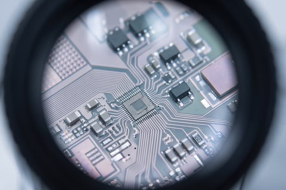
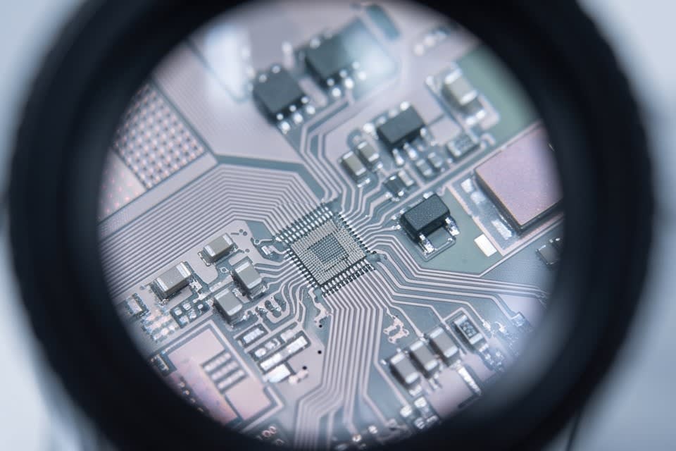
    Inspecting microscopic components on a circuit board through a magnifying glass

    In semiconductor processes, it is not uncommon for a single defect to lead to the disposal of an entire finished product. According to an analysis by Elementary ML, automated optical inspection systems can achieve defect detection rates of up to 99.5%, while visual inspection remains at a maximum of around 80%, allowing 20% of actual defects to pass through the process unchecked. This figure is not simply a comparison of performance. It is a signal that the choice of inspection method directly determines competitiveness. In semiconductor manufacturing, where precision determines yield and cost, the question of how inspection is performed carries far greater weight than it may seem.
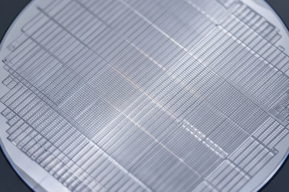
    Microscopic circuit patterns on a semiconductor wafer requiring extremely strict contamination standards

    Limitations of Visual Inspection and the Need for Automated Inspection

    In semiconductor manufacturing processes, fine particle contamination becomes more critical as feature sizes shrink. According to patents registered with the United States Patent and Trademark Office (USPTO), contamination standards are so strict that even particles as small as 5 nanometers (nm) are not acceptable in many semiconductor manufacturing processes. However, visual inspection has structural limitations in identifying contamination at this microscopic level.

    As confirmed in Instrumental’s 2024 analysis, the detection rate of visual inspection reaches only up to 80%. This means that one out of every five actual defects passes inspection. In contrast, automated optical inspection systems achieve detection rates of up to 99.5%, allowing algorithms to cover areas that the human eye can miss.

    The gap between the two methods is not merely a difference in accuracy. Given the nature of semiconductor manufacturing, where the cost of detecting defects rises exponentially in later process stages, the choice of inspection timing and method becomes a variable that changes the entire yield structure. As miniaturization continues to accelerate, the need for an inspection system that does not miss even a single particle is becoming clearer. Industry standards themselves are shifting toward automated inspection, which meets the precision requirements that visual inspection can no longer handle.
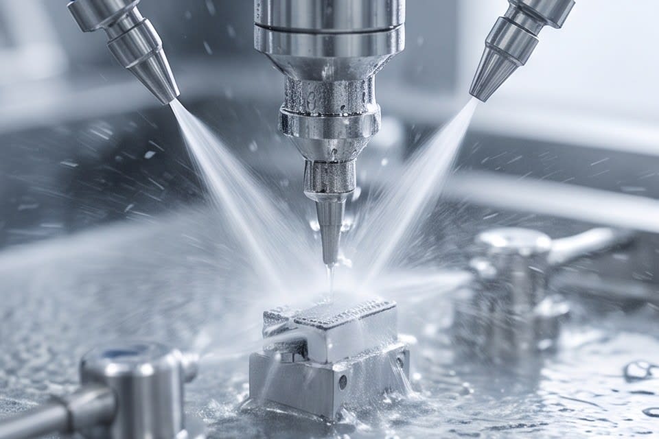
    A site where multi-stage cleaning technology is applied to remove foreign matter from component surfaces

    Integrating Cleaning and Vision Inspection into One Flow

    Operating cleaning and inspection as separate processes has a blind spot. When inspection is performed after cleaning is completed, secondary contamination generated during cleaning or particles that were not fully removed may be missed. One approach to solving this issue is to integrate the cleaning process and vision inspection algorithms into a single flow.

    Huvics cleaner systems combine multi-stage cleaning technologies such as microbubble, water jet, and air knife to remove contamination particles from product surfaces step by step. Vision inspection algorithms are integrated into this process to automatically determine surface conditions before and after cleaning. For various components with different shapes and materials, including camera modules, sensors, VCM motors, and trays, the algorithm analyzes surface images and numerically evaluates residual contamination and cleaning quality. This approach does not rely on subjective operator judgment, and creates a structure that maintains consistent quality standards within the process.

    Ultrasonic dispersion technology plays the role of uniformly dispersing contamination particles within the cleaning solution, while the vision algorithm verifies the result, making the two technologies complementary. As cleaning efficiency improves, the number of defects that inspection must filter decreases. As inspection accuracy improves, cleaning process standards can be adjusted more precisely. When cleaning and inspection form a feedback loop, overall process quality stability is implemented in a structure that improves step by step.
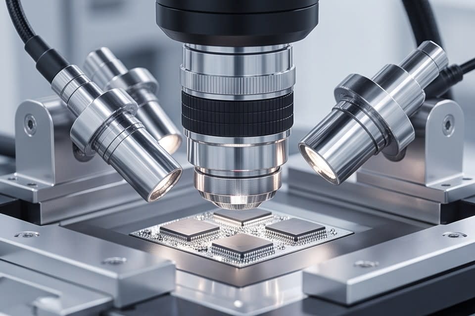
    Precisely observing the surface of electronic components at high magnification with vision inspection equipment

    The Role of Vision Inspection Algorithms Confirmed in the Field

    Huvics has confirmed through multiple field cases how the combination of vision inspection algorithms and cleaning technology changes actual defect rates in MLCC and FPCB processes.

    In the semiconductor tape bonding process, residual foreign matter after tape attachment repeatedly led to bonding defects. By linking vision inspection algorithms with the cleaning process and automatically determining surface conditions before bonding, the point at which defects were identified was moved to the early stage of the process. In camera module processes, microscopic foreign matter between the lens and image sensor was a major cause of finished product defects, and there are accumulated cases showing that solutions combining ultra-precision cleaning with algorithm-based inspection have led to reduced defect rates.

    In both cases, the cause of defects was hidden in a specific stage within the process, and the judgment criteria of the inspection algorithm played a decisive role in identifying it. In the MLCC process, ultrasonic dispersion technology suppressed the reattachment of contamination particles in the cleaning solution, while vision inspection quantitatively verified surface uniformity, improving the reproducibility of process quality.

    In any process, defect patterns repeat. Algorithms learn those repetitions as data and refine their judgment criteria. These field cases show that the combination of precision cleaning and vision inspection is not simply a combination of technologies, but an approach that changes the quality structure across the entire process.
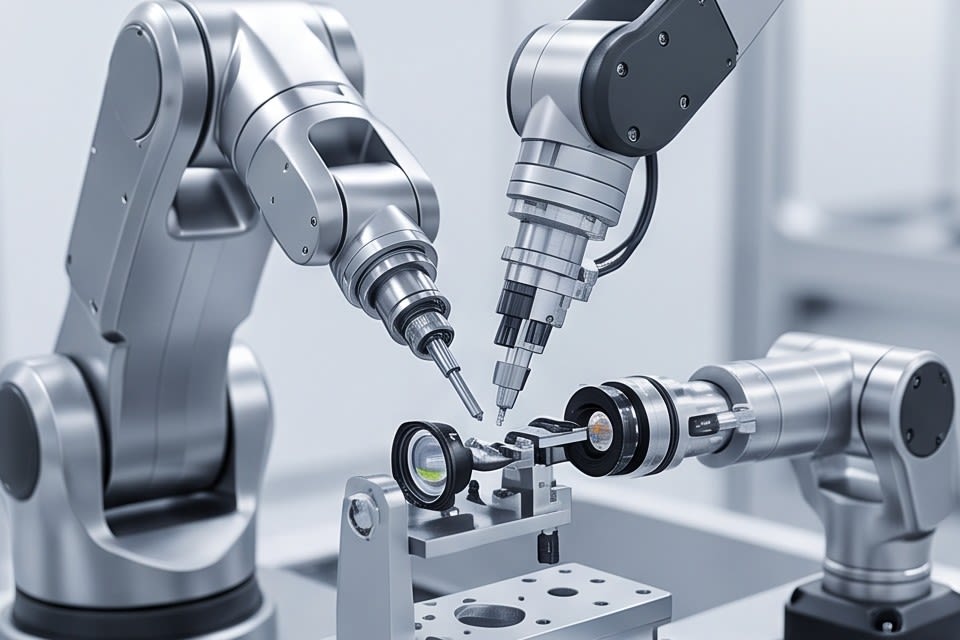
    A cleaning and inspection site where robot arms and inspection equipment are integrated to verify quality in real time

    There is a fundamental difference between a product passing inspection after cleaning is completed and inspection verifying cleaning completeness in real time. Reducing defect rates ultimately depends on when and by what standards a decision is made, and vision inspection algorithms are a means of bringing those standards into the process. When precision cleaning and algorithm-based inspection are connected into one flow, defects are filtered not at the end of the process, but within the process itself.


    Huvics is an advanced technology company that develops and manufactures automated equipment and
    production systems across the semiconductor, LED, Mobile, and Cosmetic industries.
    With top-tier talent and continuous technological innovation, we support customers in improving productivity and
    securing quality competitiveness.

    Huvics Contact

    Tel: 031-374-8285
    Email: cdpark@huvics.com

    Huvics Inquiry

  • Building Semiconductor Automation Equipment: Key Step-by-Step Process Essentials from Grinding to Cleaning

    Building Semiconductor Automation Equipment: Key Step-by-Step Process Essentials from Grinding to Cleaning

    “Opportunity comes only to those who are prepared.” This statement by Louis Pasteur applies not only to science laboratories but also directly to advanced manufacturing sites. Now that semiconductor automation equipment implementation has become a key issue, processes entered without preparation struggle to meet the yield and quality standards demanded by the market. Let us examine the specific context of which technical conditions complete readiness on the production floor.

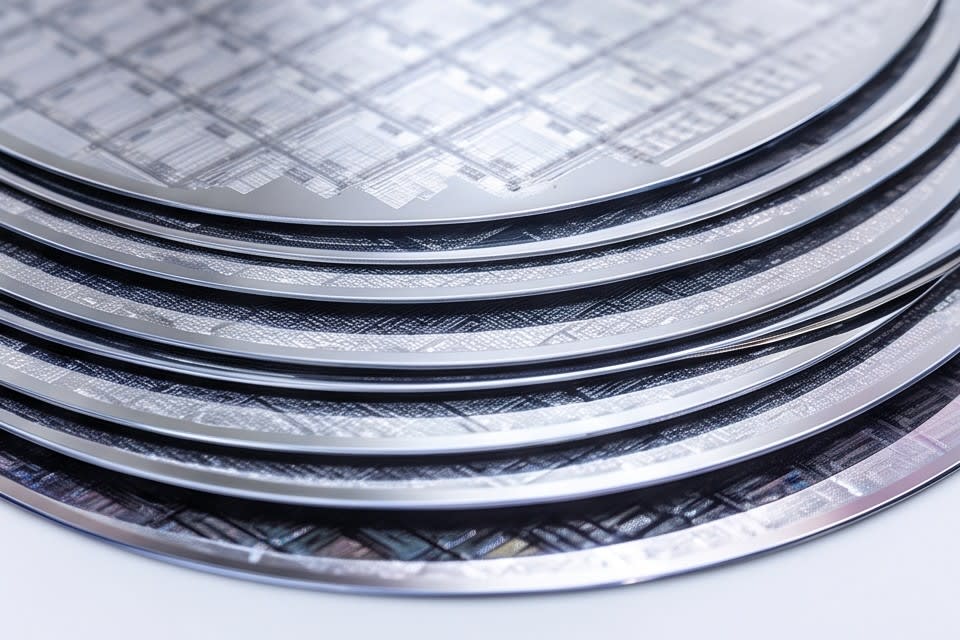
    Stacked wafers show stacking technology and flatness control in the semiconductor packaging process.

    Why the Advanced Packaging Market Demands Automation

    As demand for artificial intelligence (AI) semiconductors and high-performance memory surges, the manufacturing environment in advanced industries is being reshaped rapidly. As stacked package methods that vertically stack chips become more common, thickness uniformity and package flatness are no longer added conditions but prerequisites for design.

    According to a market analysis released by OEMstron, the advanced packaging market is expected to grow from about 53.1 billion dollars in 2025 to 79.4 billion dollars in 2030, with a compound annual growth rate of 8.4%. In the same trend, the flip chip ball grid array (FCBGA) market is also expected to expand from about 5.355 billion dollars in 2024 to around 10 billion dollars in 2031.

    These figures are not simply statistics on market growth. They are also a signal that entering this market is difficult without precise process control. A single package type contains dozens of process variables, and if even one of them moves outside the allowable range, the entire yield becomes unstable. The trend in which automation equipment implementation has become an entry requirement rather than an option is already clear across the market.

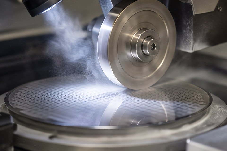
    A diamond wheel is precisely grinding a wafer on the stage at the micron level.

    Technical Principles of Grinding and Lamination Processes

    In semiconductor automation equipment implementation, the order of the process is directly linked to the order of quality. Grinding, lamination, and cleaning and drying must connect as one continuous flow for final yield to remain stable.

    The grinding process uniformly reduces package thickness at the micron (μm, one thousandth of 1 mm) level. Using a diamond wheel and a high-precision stage, it supports various package types such as FCBGA, wafer level chip scale package (WLCSP), and quad flat no lead or dual flat no lead (QFN/DFN). Even a small thickness deviation can lead to bonding defects or reduced electrical reliability in later processes, so equipment design that minimizes deviation even in high-speed processing is essential. The Huvics PKG grinder implements this principle in both Full Auto and Manual methods, ensuring flexibility for production lines.

    The lamination process simplifies production by handling everything from tape attachment to ultraviolet (UV) curing within a single system. A structure that connects one-stop from the Expander to UV curing reduces transfer time between processes and shortens Tact Time, the time required to complete one product. Academic research has also reported analysis results showing that an automated yield improvement framework can raise efficiency by about 17.6% compared with traditional manual methods. The precision and continuity of each process step ultimately determine the overall yield.

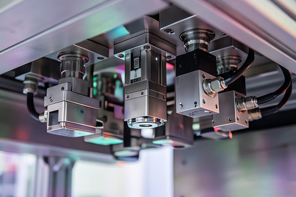
    This shows the sophisticated sensor and nozzle configuration inside equipment designed to control fine contamination particles.

    How the Cleaning Process Completes Final Quality

    The cleaning process often receives attention last in semiconductor automation equipment implementation, but it is in fact the step that determines final quality. No matter how precisely grinding and lamination are performed, defects can occur in later processes if fine contamination particles remain on the surface. For components that are extremely sensitive to contamination, such as camera modules, vibration control motors (VCM motors), and various sensors, the reliability of the cleaning stage determines shipment quality.

    A multi-stage cleaning method that combines Micro Bubble, Water Jet, and Air Knife removes surface contamination particles step by step while minimizing physical impact on the material. According to a study published on ResearchGate, optimizing droplet diameter in a physical cleaning process can achieve a particle removal efficiency of 92.9%.

    Actual production sites have also accumulated cases in which defects repeatedly occurring in semiconductor tape bonding processes were resolved simply by redesigning cleaning conditions, as well as cases in which camera module defect rates dropped noticeably after the introduction of precision cleaning. A configuration that integrates oven drying after cleaning also blocks the possibility of secondary defects caused by residual moisture. This confirms that how precisely the final stage of the process is completed gives meaning to the value of all preceding processes.

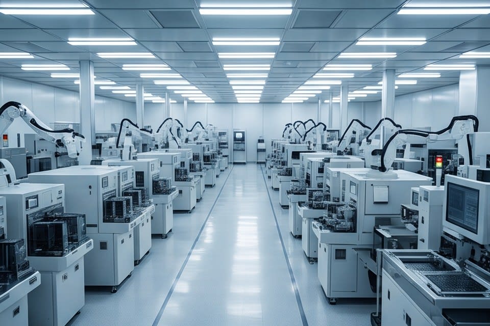
    A panoramic view of a large-scale automation line at a semiconductor manufacturing site where multiple process units are organically connected.

    Semiconductor automation equipment implementation cannot be completed through the excellence of any single process alone. Only when grinding precision, lamination continuity, and cleaning reliability connect as one flow can yield and quality stabilize together. The standards demanded by the market continue to rise, and process design that meets those standards becomes the practical competitiveness of advanced industrial sites.


    Huvics is an advanced technology company that develops and manufactures automation equipment and
    production systems across the semiconductor, LED, Mobile, and Cosmetic industries.
    With top talent and continuous technological innovation, we support customers in improving productivity and
    securing quality competitiveness.

    Huvics Contact

    Phone: 031-374-8285
    Email: cdpark@huvics.com
    Huvics inquiry

  • Huvics Precision Machining Solutions – Customized Strategies Driving Innovation on the Manufacturing Floor and the Foundation of Future Technology

    Huvics Precision Machining Solutions – Customized Strategies Driving Innovation on the Manufacturing Floor and the Foundation of Future Technology

    Huvics

    Do you ever feel uneasy that your factory’s production efficiency may not be keeping pace with technological progress? In a rapidly changing global market, simply introducing new equipment inevitably reaches its limits.

    Manufacturing sites now require more than speed. They demand insight and strategic partnerships that can solve complex challenges with precision. Discover the distinctive answer to how Huvics, at the forefront of precision machining, is transforming customers’ process infrastructure and building a solid foundation for future technology.

    Huvics integrated solution

    Total Solutions for Innovation on the Manufacturing Floor

    Customized Strategies to Maximize Production Efficiency

    The true competitiveness of a manufacturing site does not come merely from increasing production speed. Today’s manufacturing environment is becoming increasingly complex, and customer expectations for quality continue to rise day by day.

    In this environment, simply supplying machining equipment is not enough to keep up with market change. Beyond being a hardware supplier, Huvics focuses on deeply analyzing the entire manufacturing process of each customer and designing total customized solutions that maximize production efficiency.

    Efficient automated process

    Securing Manufacturing Competitiveness Through Technical Support

    By resolving complex and demanding challenges that arise on site with precision machining technology, Huvics provides close technical support throughout the entire process so that customers can secure the highest levels of quality and productivity. This becomes a practical driving force that helps customers minimize trial and error and focus on the essential value of manufacturing.

    Even amid rapidly changing technology trends, Huvics solutions serve as a strong strategic foundation that helps manufacturers achieve sustainable growth and a distinctive competitive edge. They play a key role in building the foundation for new future technologies that go beyond the limits of manufacturing.

    Precision machining technology capabilities

    Distinctive Expertise and Strategic Partnerships

    Technical Data Proven in Global Industrial Sites

    The strength of Huvics is rooted in distinctive expertise gained by completing numerous projects in the most dynamic fields with the strictest standards, including global IT and automotive electronics industries. We analyze years of accumulated precision machining technical data and success cases from multiple perspectives to present the most effective and optimized customized strategies for the individual challenges faced by each customer.

    A Strategic Partner Driving Business Growth

    The insight to identify and analyze market technology trends and rising customer requirements one step ahead is a powerful differentiator unique to Huvics. Going beyond the supplier role of simply providing technology, we continue to innovate as a strategic partner that thinks through each customer’s business journey together and drives tangible results.

    Advanced robot system

    Building Future-Oriented Process Infrastructure

    Process Optimization for Sustainable Growth

    Ultimately, the goal Huvics pursues is to help customers build robust and flexible process infrastructure that enables them to lead market changes on their own. The precision machining solutions we provide do not stop at short-term results that optimize current processes. They become a solid foundation and cornerstone for turning the possibilities of future technology into reality.

    Technology Innovation for a Clear Competitive Advantage

    Huvics technological innovation, which continuously breaks through the physical limits of manufacturing processes and maximizes efficiency, supports customers in securing a clear and stable advantage in highly competitive markets. Only companies that respond with agility on a stable production foundation can continue to grow through any external market change.

    With the unwavering belief that our customers’ success is our success, Huvics will continue to add new value to your business as a future-oriented partner leading innovation on the manufacturing floor.

    Recommendations for Successful Manufacturing Sites

    The success of a manufacturing site depends on the precision required to find the optimal answer within complex processes. Discover how the customized solutions proposed by Huvics can add greater value and growth momentum to your manufacturing site.


    Huvics is an advanced technology company that develops and manufactures automation equipment and
    production systems across the semiconductor, LED, Mobile, and Cosmetic industries.
    Through top-tier talent and continuous technological innovation, we support customers in improving productivity and
    securing quality competitiveness.

    Huvics Contact Information

    Phone: 031-374-8285
    Email: cdpark@huvics.com
    Huvics inquiry