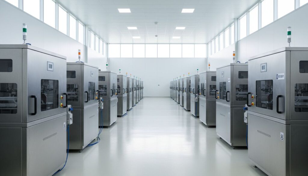
“Opportunity comes only to those who are prepared.” This statement by Louis Pasteur applies not only to science laboratories but also directly to advanced manufacturing sites. Now that semiconductor automation equipment implementation has become a key issue, processes entered without preparation struggle to meet the yield and quality standards demanded by the market. Let us examine the specific context of which technical conditions complete readiness on the production floor.
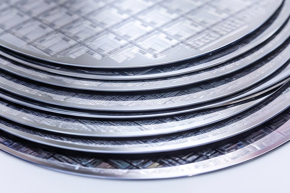
Why the Advanced Packaging Market Demands Automation
As demand for artificial intelligence (AI) semiconductors and high-performance memory surges, the manufacturing environment in advanced industries is being reshaped rapidly. As stacked package methods that vertically stack chips become more common, thickness uniformity and package flatness are no longer added conditions but prerequisites for design.
According to a market analysis released by OEMstron, the advanced packaging market is expected to grow from about 53.1 billion dollars in 2025 to 79.4 billion dollars in 2030, with a compound annual growth rate of 8.4%. In the same trend, the flip chip ball grid array (FCBGA) market is also expected to expand from about 5.355 billion dollars in 2024 to around 10 billion dollars in 2031.
These figures are not simply statistics on market growth. They are also a signal that entering this market is difficult without precise process control. A single package type contains dozens of process variables, and if even one of them moves outside the allowable range, the entire yield becomes unstable. The trend in which automation equipment implementation has become an entry requirement rather than an option is already clear across the market.
Technical Principles of Grinding and Lamination Processes
In semiconductor automation equipment implementation, the order of the process is directly linked to the order of quality. Grinding, lamination, and cleaning and drying must connect as one continuous flow for final yield to remain stable.
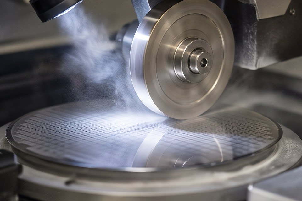
The grinding process uniformly reduces package thickness at the micron (μm, one thousandth of 1 mm) level. Using a diamond wheel and a high-precision stage, it supports various package types such as FCBGA, wafer level chip scale package (WLCSP), and quad flat no lead or dual flat no lead (QFN/DFN). Even a small thickness deviation can lead to bonding defects or reduced electrical reliability in later processes, so equipment design that minimizes deviation even in high-speed processing is essential. The Huvics PKG grinder implements this principle in both Full Auto and Manual methods, ensuring flexibility for production lines.
The lamination process simplifies production by handling everything from tape attachment to ultraviolet (UV) curing within a single system. A structure that connects one-stop from the Expander to UV curing reduces transfer time between processes and shortens Tact Time, the time required to complete one product. Academic research has also reported analysis results showing that an automated yield improvement framework can raise efficiency by about 17.6% compared with traditional manual methods. The precision and continuity of each process step ultimately determine the overall yield.
How the Cleaning Process Completes Final Quality
The cleaning process often receives attention last in semiconductor automation equipment implementation, but it is in fact the step that determines final quality. No matter how precisely grinding and lamination are performed, defects can occur in later processes if fine contamination particles remain on the surface. For components that are extremely sensitive to contamination, such as camera modules, vibration control motors (VCM motors), and various sensors, the reliability of the cleaning stage determines shipment quality.
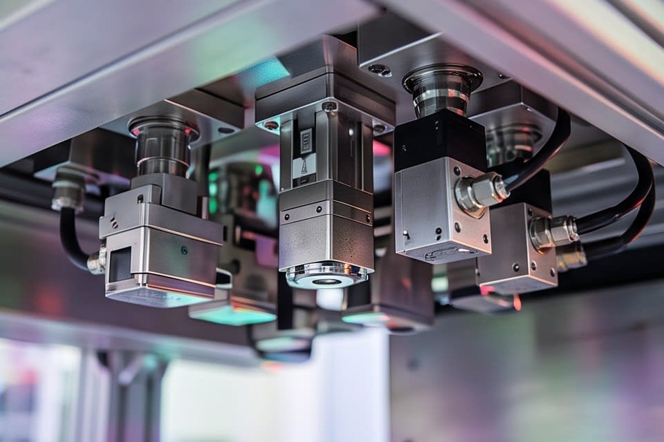
A multi-stage cleaning method that combines Micro Bubble, Water Jet, and Air Knife removes surface contamination particles step by step while minimizing physical impact on the material. According to a study published on ResearchGate, optimizing droplet diameter in a physical cleaning process can achieve a particle removal efficiency of 92.9%.
Actual production sites have also accumulated cases in which defects repeatedly occurring in semiconductor tape bonding processes were resolved simply by redesigning cleaning conditions, as well as cases in which camera module defect rates dropped noticeably after the introduction of precision cleaning. A configuration that integrates oven drying after cleaning also blocks the possibility of secondary defects caused by residual moisture. This confirms that how precisely the final stage of the process is completed gives meaning to the value of all preceding processes.
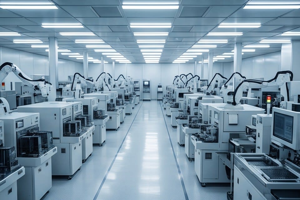
Semiconductor automation equipment implementation cannot be completed through the excellence of any single process alone. Only when grinding precision, lamination continuity, and cleaning reliability connect as one flow can yield and quality stabilize together. The standards demanded by the market continue to rise, and process design that meets those standards becomes the practical competitiveness of advanced industrial sites.
Huvics is an advanced technology company that develops and manufactures automation equipment and
production systems across the semiconductor, LED, Mobile, and Cosmetic industries.
With top talent and continuous technological innovation, we support customers in improving productivity and
securing quality competitiveness.
Huvics Contact
Phone: 031-374-8285
Email: cdpark@huvics.com