Tag: technological innovation

  • AI Semiconductor Stacked Packages: Why the Grinding Process Became the Starting Point for Yield

    AI Semiconductor Stacked Packages: Why the Grinding Process Became the Starting Point for Yield

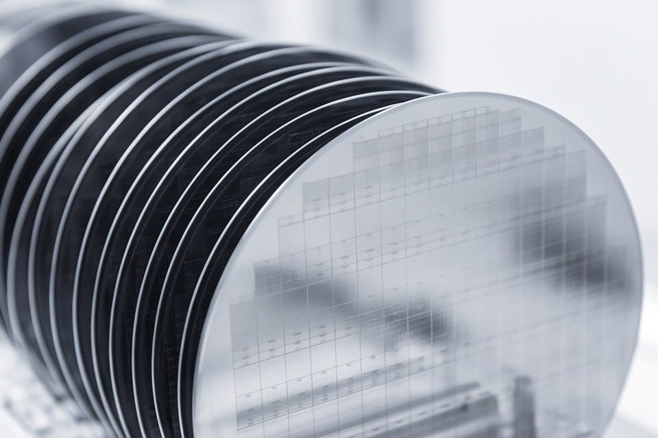
    Multiple wafers stacked vertically

    In semiconductor packaging, controlling thickness was long regarded as simply grinding materials thin enough. However, with the arrival of high-performance artificial intelligence semiconductors that stack multiple chip layers, that standard has changed completely. Simply making the material thinner is no longer enough to ensure bonding reliability in stacked structures, and minute thickness variations in each layer can accumulate and affect the performance of the entire package. Today, a completely different level of grinding technology is required, one that can secure micron-level uniformity and flatness at the same time.

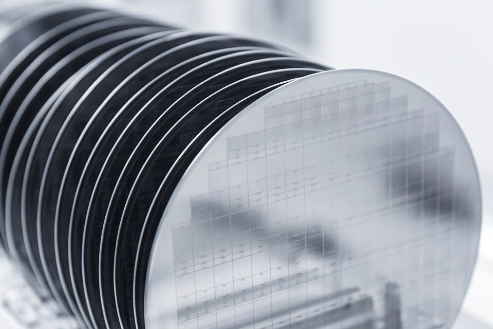
    Cross section of wafers stacked vertically in multiple layers

    Why Thickness Uniformity Becomes a Prerequisite in Stacked Packages

    In stacked package structures where dozens of chips are piled vertically, thickness variation in each layer is not merely a dimensional issue. The more precisely designed the package substrate structure is, as in FCBGA(Flip Chip Ball Grid Array) or WLCSP(Wafer Level Chip Scale Package), the more the uniformity of remaining thickness after grinding becomes a prerequisite for all subsequent processes.

    In particular, WLCSP eliminates the substrate and mounts the chip directly onto the main board, so the impact of grinding precision appears immediately in electrical characteristics as the signal path becomes shorter. According to data from the United States Patent and Trademark Office(USPTO), the current target thickness for wafer backside grinding is about 300μm(microns), and it is expected to become even thinner in the 200 to 250μm range going forward. As the thickness target becomes lower, the allowable margin of error also becomes narrower, while the level of precision required in the process increases inversely. In this trend, the role of the grinding process is increasingly becoming a key variable in packaging quality.
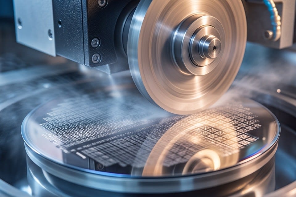
    A semiconductor wafer rotating while being precision ground by a diamond wheel

    The Two-Step Structure and Tolerance Standards of Precision Grinding

    To understand the tolerance level required by precision grinding, a sense of proportion is more important than the numbers themselves. The allowable tolerance required in grinding for semiconductor manufacturing equipment is about ±2.54μm(microns), which is only a few dozenths of the thickness of a human hair, considering that human hair is about 70 to 100μm thick.

    To reliably achieve this level of precision, commercial grinding systems operate two process stages in sequence.

    • Coarse grinding stage: Rapidly removes material at a speed of about 5μm per second.
    • Fine grinding stage: Reduces the speed to 1μm per second or less to secure surface roughness and thickness uniformity.

    Reducing speed is the core principle for increasing precision, and how precisely the transition point and conditions between the two stages are controlled is the key factor that determines final yield. Equipment configuration that combines a diamond wheel with a high-precision stage is the core hardware that reliably supports this transition process, and the completeness of equipment design is directly revealed under conditions that must satisfy both fine tolerance control and repeatable reproducibility.

    Precisely processed semiconductor packages arranged on a tray

    How PKG Grinder Responds to On-Site Conditions

    When introducing grinding equipment at an AI semiconductor packaging site, the first practical question is “which package types can it support”. In many cases, a single production line must handle multiple packages at the same time, including FCBGA, WLCSP, and QFN/DFN(Quad Flat No Lead), while the target thickness required by customers differs by product.

    Huvics PKG Grinder is designed for these on-site conditions with Full Auto A/B types and Manual type options, allowing flexible selection according to the automation level of the production line and the characteristics of the product. Processing uniformly and precisely to the thickness customers require is not simply a matter of equipment specifications. It means the equipment must allow settings that reflect actual process conditions and package structures.

    The requirement to maintain stable yield even during high-speed processes in manufacturing sites that handle ultra-precision components, such as camera modules or autonomous driving sensors, directly shows how important repeatable reproducibility and in-process consistency are for equipment. As stacked structures become more complex and target thickness becomes thinner, the range of precision that grinding equipment must handle also expands. This is where the significance of PKG Grinder in this process becomes clear.
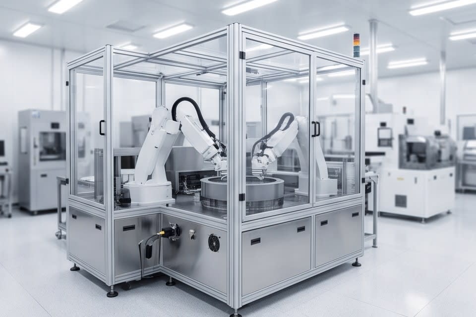
    Exterior of an automated grinding system installed in a cleanroom environment

    The complexity of stacked structures required by AI semiconductors has transformed the grinding process from a simple post-processing step into the starting point of quality. The ability to repeatedly achieve micron-level tolerances ultimately shows where the reliability and yield of the entire package are determined. As thickness targets become thinner and the number of stacked layers increases, the demand for grinding precision will continue to rise.


    Huvics is an advanced technology company that develops and manufactures automation equipment and
    production systems across the semiconductor, LED, Mobile, and Cosmetic industries.
    With top-level talent and continuous technological innovation, we support customers in improving productivity and
    securing quality competitiveness.

    Huvics Contact Information

    Phone: 031-374-8285
    Email: cdpark@huvics.com

    Huvics Inquiry

  • Why the Early Stage of the Semiconductor Process Matters – Technical Insights and Strategic Value Presented by Huvics

    Why the Early Stage of the Semiconductor Process Matters – Technical Insights and Strategic Value Presented by Huvics

    Huvics

    In semiconductor manufacturing, where ultrafine circuits at the nanometer scale are realized, why do global technology experts point to the very beginning of the process as the most critical battleground above all else? In today’s environment, where even one invisible microscopic particle can disrupt the entire yield, precise cleaning and control in the early stage have become not just a process sequence but a core strategy that determines a company’s survival.

    This is precisely the area Huvics focuses on, having proven its technological reliability in the global market by receiving the USD 1 Million Export Tower award on Trade Day 2025. Let us take a closer look at the decisive insights Huvics has gained in the field, and how the future of semiconductors changes depending on how perfectly the first step of the process is executed.

    View of a semiconductor cleanroom

    The Core of the Semiconductor Process, the Importance of the Early Stage

    The Golden Time That Determines Process Success

    In the vast and complex world of semiconductor manufacturing, why do experts focus so persistently on the beginning, or early stage, of the process? This goes beyond simply being the first step in sequence. It is the decisive golden time that determines the success or failure of the entire production process.

    Today, as semiconductor circuits have become extremely miniaturized to the nanometer scale, even one tiny particle that is difficult to detect under a microscope can shake the reliability of the entire product. How completely and precisely impurities are removed in the early stage of the process directly becomes the most essential indicator that determines final yield.

    Huvics’ Precision Cleaning and Efficiency Maximization

    Huvics deeply understands the importance of this early process and concentrates all its capabilities on strengthening the foundation of the process through precision cleaning technology and advanced automated equipment. Thorough contamination control in the early stage dramatically reduces the complexity of subsequent processes and ultimately creates a powerful virtuous cycle that maximizes the efficiency of the entire production line.

    With years of accumulated proprietary patented technologies and field-centered know-how, Huvics pursues perfection from the very first step of the process as a strategic partner that solves the challenges of semiconductor manufacturing, driving global technological competitiveness.

    Core of precision cleaning technology

    Huvics’ Technology Recognized by the Global Market

    Unique Capabilities and Risk Prevention

    The reason companies like Huvics, which have proven technological reliability, are recognized as key problem solvers in the fiercely competitive global manufacturing field is their unique capability to overcome the high technological barriers present in the early stage of the process. Huvics, which proved its capabilities in the global market by receiving the USD 1 Million Export Tower award on Trade Day 2025, completely blocks potential risks hidden in the early stage of the process in advance, based on numerous patented technologies accumulated over many years and extensive field project experience.

    Value as a Strategic Partner

    This goes beyond the general level of manufacturing support that simply supplies equipment. It carries a highly strategic value by helping customers secure a strong competitive advantage from the starting point of their manufacturing processes. Through continuous research and development investment, Huvics has steadily expanded its portfolio in precision cleaning and automation, and even now works alongside global companies to solve diverse challenges while serving as the most reliable partner in building stable mass production systems.

    Controlling unexpected variables in advance within complex manufacturing processes not only prevents economic losses for companies but also becomes the most reliable line of defense for protecting market share over the long term.

    Advanced automated equipment

    The Technical Standard of the Future Semiconductor Industry

    Securing Market Competitiveness Through Technological Innovation

    The future semiconductor industry will be rapidly reshaped around advanced precision cleaning and automation technologies that go beyond existing limits. Ultimately, the technological gap in the early process will become a key variable that determines a company’s market competitiveness, and this will lead to raising the technical standards of the entire semiconductor ecosystem by one level, beyond simple improvements in manufacturing efficiency.

    Huvics is taking the lead in this change by expanding its portfolio in precision cleaning and automation through continuous research and development investment. We clearly understand that securing the completeness of the early process without any gaps is the most reliable strategy for surviving in the next generation IT manufacturing market and leading innovation.

    Huvics’ Path as a Global Milestone

    With Huvics, which continues to drive the future competitiveness of semiconductors through ongoing technological innovation, customers can design a future one step ahead from the very starting point of the process. Huvics’ steps toward creating global standards based on technological reliability are becoming a new milestone not only for Korea but also for the global semiconductor manufacturing market, and they will remain at the center of continued change.

    Standard of the semiconductor ecosystem

    Expert Recommendations for a Successful Manufacturing Environment

    A Technical Foundation for High-Quality Mass Production

    The reason we must once again recognize the importance of the early stage of the semiconductor process is that the speed of technological progress is incomparably faster than before. As microprocesses become more advanced, the precision of early cleaning serves as a shield that prevents product defects and, at the same time, as an engine that enables high-quality mass production.

    Huvics goes beyond being a company that simply supplies equipment. It pursues value as a group of experts that analyzes process flows, predicts potential errors, and presents optimal solutions. It is an unchanging rule of the industry that the performance of the latest semiconductor devices can be fully realized only on a clean foundation secured in the early process.

    Partnership for Sustainable Growth

    Going forward, Huvics will continue to devote its full efforts to helping customers overcome manufacturing limitations through technology and to providing a successful manufacturing environment where the beginning of the process leads directly to the best results. These continuous efforts will ultimately enhance the brand value of customers and become a key contribution that accelerates the development of the entire semiconductor manufacturing industry.

    The future of semiconductors we envision begins at this very moment, with the commitment to perfecting the very first step of the process.

    Stable mass production system

    Conclusion

    Ultimately, we have clearly confirmed that the success or failure of semiconductor manufacturing does not begin with the sum of countless processes, but with a perfectly prepared first step. Huvics’ precision cleaning technology and automation solutions, proven through the USD 1 Million Export Tower award on Trade Day 2025, go beyond simple manufacturing support and serve as a strategic shield that solves the challenges customers face and ensures optimal yield.

    Huvics’ rigorous standards, which do not tolerate even the smallest invisible defect, will soon become the new standard in the next generation semiconductor market. Now that the starting point of the process is directly becoming a company’s future competitiveness, we invite you to complete a stable manufacturing ecosystem together with Huvics, which guarantees technological reliability.


    Huvics is an advanced technology company that develops and manufactures automation equipment and
    production systems across the semiconductor, LED, Mobile, and Cosmetic industries.
    With outstanding talent and continuous technological innovation, we support customers in improving productivity and
    securing quality competitiveness.

    Huvics Contact Information

    Phone: 031-374-8285
    Email: cdpark@huvics.com

    Huvics Inquiry

  • A Strategic Partner for Improving Productivity in Semiconductor Manufacturing Processes, Huvics Customized Engineering Solutions

    A Strategic Partner for Improving Productivity in Semiconductor Manufacturing Processes, Huvics Customized Engineering Solutions

    Huvics

    In semiconductor manufacturing, where a 1 percent difference in yield can determine a company’s survival, are you now looking for the most reliable breakthrough? In a fierce process battlefield where even the slightest momentary error cannot be tolerated, maximizing production efficiency with limited resources and securing leadership in the global market are core challenges for every company.

    Huvics, which proved its technological capabilities on the global stage by receiving the 1 Million Dollar Export Tower on Trade Day in 2025, presents the answer as a strategic partner that goes beyond simple equipment supply to transform the very structure of manufacturing processes. Let us now explore how Huvics resolves bottlenecks in complex processes and completes the unmatched competitiveness of its customers.

    Maximizing semiconductor yield and production efficiency

    Huvics Technology and Core Capabilities

    The semiconductor manufacturing site is like a battlefield of precision and speed where not even the smallest error is allowed. In an environment where yield and production efficiency determined in a fleeting moment can decide the fate of a company, Huvics has established itself as a key partner leading innovation in the global semiconductor and advanced IT industries. In particular, the achievement of receiving the 1 Million Dollar Export Tower on Trade Day in 2025 became an important milestone that objectively proved its technology and reliability on the world stage.

    This achievement means that Huvics technology is being converted into real productivity at manufacturing sites around the world. The core capabilities through which Huvics has built customer trust are as follows.

    • Solving complex and challenging process issues based on an extensive patent portfolio accumulated over many years
    • Analyzing manufacturing processes in a multidimensional way using field-centered practical project experience as an asset
    • Providing customized engineering solutions that fundamentally remove process bottlenecks

    Precise semiconductor automation solutions

    Strategic Approach for Manufacturing Process Optimization

    Rapidly changing semiconductor technology trends and an increasingly competitive global market environment require manufacturers to make highly strategic decisions for survival beyond simple quantitative growth. The biggest challenge companies face is optimizing the entire manufacturing process with limited resources to improve yield and maximize production efficiency. Huvics functions as a practical partner that solves customer concerns at the closest point to the field.

    Strategy for Maximizing Process Potential

    Beyond the general approach of simply diagnosing current conditions and placing equipment, we take a strategic approach that draws out the full potential of the process. This approach not only protects manufacturers’ technological superiority but also serves as the foundation for firmly establishing an unmatched market share in the global market.

    Multidimensional process analysis and management

    Engineering Solutions for Sustainable Growth

    Every process with Huvics will become a source of confidence that fundamentally improves the structure of manufacturing processes and lays the groundwork for sustainable growth that remains stable amid market changes. The innovative engineering solutions we provide go beyond tools that simply increase efficiency. They are the most reliable competitive advantage and a stable alternative that helps customers maintain leadership in future industries.

    Customized engineering design

    Recommendations for Securing Manufacturing Competitiveness

    In the fierce competition of the semiconductor industry, overcoming technological limits is no longer a choice but a matter of survival. Huvics proven engineering solutions, demonstrated by the 2025 Trade Day 1 Million Dollar Export Tower award, will become a reliable partner that fundamentally improves the structure of your processes and helps your company secure unmatched technological superiority in the global market.

    Simply resolving the bottlenecks you face today can dramatically improve production efficiency, and Huvics is ready to present the optimal answer. We hope you secure a higher level of manufacturing competitiveness together with an innovative partner and build your own sustainable future amid a rapidly changing industrial environment.

    Innovation at global manufacturing sites


    Huvics is an advanced technology company that develops and manufactures automation equipment and
    production systems across the semiconductor, LED, mobile, and cosmetic industries.
    With top-tier talent and continuous technological innovation, we support customers in improving productivity and
    securing quality competitiveness.

    Huvics Contact

    Phone: 031-374-8285
    Email: cdpark@huvics.com

    Huvics Inquiry