In semiconductor packaging, controlling thickness was long regarded as simply grinding materials thin enough. However, with the arrival of high-performance artificial intelligence semiconductors that stack multiple chip layers, that standard has changed completely. Simply making the material thinner is no longer enough to ensure bonding reliability in stacked structures, and minute thickness variations in each layer can accumulate and affect the performance of the entire package. Today, a completely different level of grinding technology is required, one that can secure micron-level uniformity and flatness at the same time.

Why Thickness Uniformity Becomes a Prerequisite in Stacked Packages
In stacked package structures where dozens of chips are piled vertically, thickness variation in each layer is not merely a dimensional issue. The more precisely designed the package substrate structure is, as in FCBGA(Flip Chip Ball Grid Array) or WLCSP(Wafer Level Chip Scale Package), the more the uniformity of remaining thickness after grinding becomes a prerequisite for all subsequent processes.
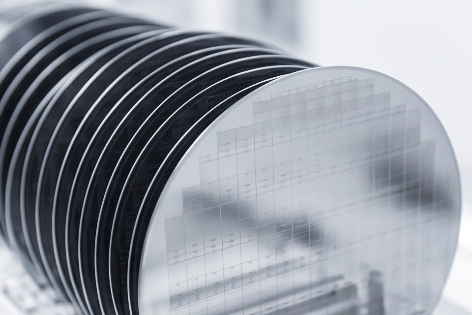
In particular, WLCSP eliminates the substrate and mounts the chip directly onto the main board, so the impact of grinding precision appears immediately in electrical characteristics as the signal path becomes shorter. According to data from the United States Patent and Trademark Office(USPTO), the current target thickness for wafer backside grinding is about 300μm(microns), and it is expected to become even thinner in the 200 to 250μm range going forward. As the thickness target becomes lower, the allowable margin of error also becomes narrower, while the level of precision required in the process increases inversely. In this trend, the role of the grinding process is increasingly becoming a key variable in packaging quality.

The Two-Step Structure and Tolerance Standards of Precision Grinding
To understand the tolerance level required by precision grinding, a sense of proportion is more important than the numbers themselves. The allowable tolerance required in grinding for semiconductor manufacturing equipment is about ±2.54μm(microns), which is only a few dozenths of the thickness of a human hair, considering that human hair is about 70 to 100μm thick.
To reliably achieve this level of precision, commercial grinding systems operate two process stages in sequence.
- Coarse grinding stage: Rapidly removes material at a speed of about 5μm per second.
- Fine grinding stage: Reduces the speed to 1μm per second or less to secure surface roughness and thickness uniformity.
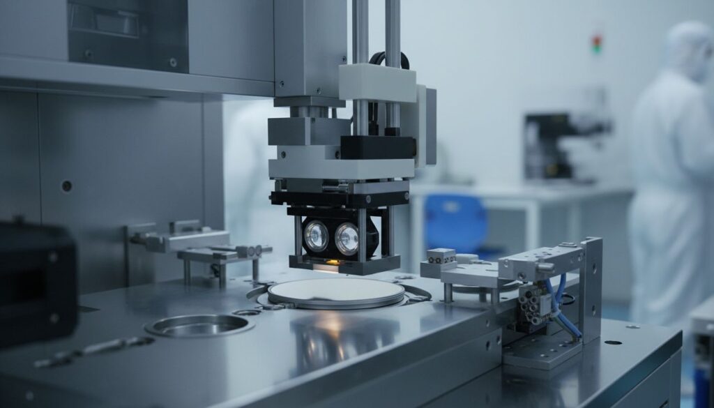
Reducing speed is the core principle for increasing precision, and how precisely the transition point and conditions between the two stages are controlled is the key factor that determines final yield. Equipment configuration that combines a diamond wheel with a high-precision stage is the core hardware that reliably supports this transition process, and the completeness of equipment design is directly revealed under conditions that must satisfy both fine tolerance control and repeatable reproducibility.

How PKG Grinder Responds to On-Site Conditions
When introducing grinding equipment at an AI semiconductor packaging site, the first practical question is “which package types can it support”. In many cases, a single production line must handle multiple packages at the same time, including FCBGA, WLCSP, and QFN/DFN(Quad Flat No Lead), while the target thickness required by customers differs by product.
Huvics PKG Grinder is designed for these on-site conditions with Full Auto A/B types and Manual type options, allowing flexible selection according to the automation level of the production line and the characteristics of the product. Processing uniformly and precisely to the thickness customers require is not simply a matter of equipment specifications. It means the equipment must allow settings that reflect actual process conditions and package structures.
The requirement to maintain stable yield even during high-speed processes in manufacturing sites that handle ultra-precision components, such as camera modules or autonomous driving sensors, directly shows how important repeatable reproducibility and in-process consistency are for equipment. As stacked structures become more complex and target thickness becomes thinner, the range of precision that grinding equipment must handle also expands. This is where the significance of PKG Grinder in this process becomes clear.

The complexity of stacked structures required by AI semiconductors has transformed the grinding process from a simple post-processing step into the starting point of quality. The ability to repeatedly achieve micron-level tolerances ultimately shows where the reliability and yield of the entire package are determined. As thickness targets become thinner and the number of stacked layers increases, the demand for grinding precision will continue to rise.
Huvics is an advanced technology company that develops and manufactures automation equipment and
production systems across the semiconductor, LED, Mobile, and Cosmetic industries.
With top-level talent and continuous technological innovation, we support customers in improving productivity and
securing quality competitiveness.
Huvics Contact Information
Phone: 031-374-8285
Email: cdpark@huvics.com