Tag: yield improvement

  • When 1 Micron Determines Yield in the Field: Key Insights into the Chip Stacking Grinding Process

    When 1 Micron Determines Yield in the Field: Key Insights into the Chip Stacking Grinding Process

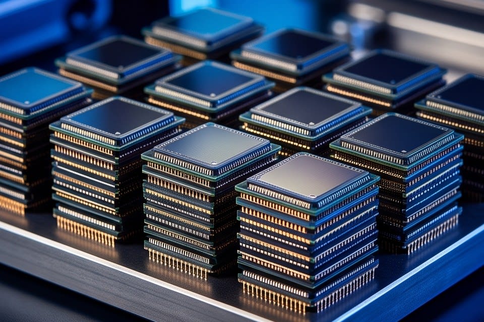
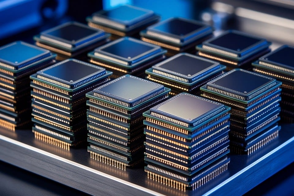
    Semiconductor chips neatly aligned and vertically stacked.

    There is a joke often shared among semiconductor design engineers. “The more chips you stack, the better, but the problem is that stacking them is far too difficult.” In real packaging processes where dozens of chip layers are stacked, the first thing to fail is not the design drawing, but flatness. In a world where a 1 micron difference can disrupt overall yield, the meaning of “grinding well” carries far more weight than expected.
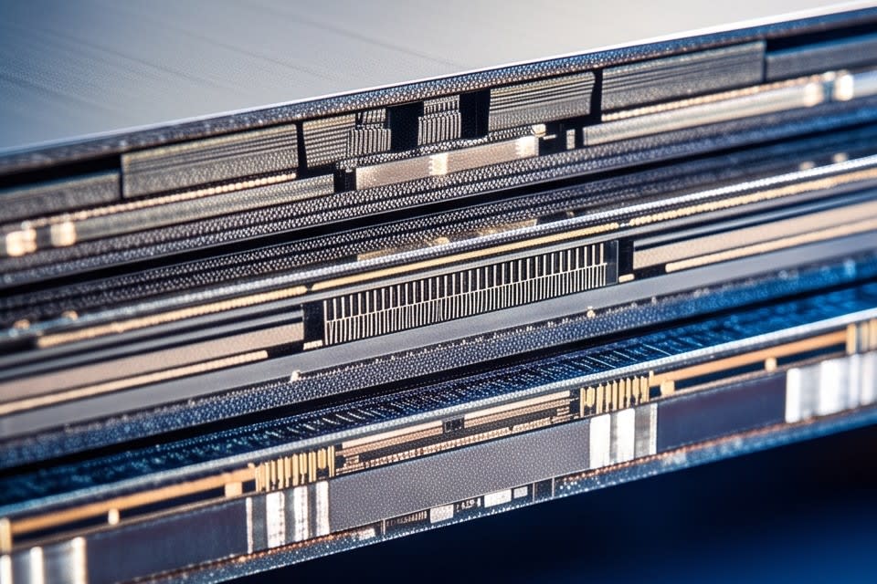
    A cross section of semiconductor chips precisely stacked with microscopic spacing.

    Why TTV Matters in Chip Stacking Structures

    In structures where chips are stacked in multiple layers, thickness variation in each layer is not just a dimensional issue. As layers accumulate, microscopic errors build up and eventually lead to electrical bonding defects or concentrated structural stress. The metric used to express this numerically is total thickness variation, or TTV.

    The TTV required in chip stacking structures is at the level of 1 micron or less, demanding precision far below one hundredth of the thickness of a human hair. If this standard is not met, bonding surfaces can lift during subsequent bonding processes or heat dissipation can become uneven, undermining the reliability of the device itself. For products such as AI semiconductors or high performance memory that vertically connect dozens of chips, the allowable variation range becomes even narrower.

    One reason TTV control is difficult in the field is the structural variables of the grinding equipment itself. The wear pattern of the grinding wheel, microscopic vibration generated during spindle rotation, and changes in the flatness of the chuck that fixes the wafer act together to make the thickness profile uneven. Uniform flatness cannot be achieved simply by turning on the equipment. How precisely these variables are controlled is the key factor that determines the yield of the entire packaging process.
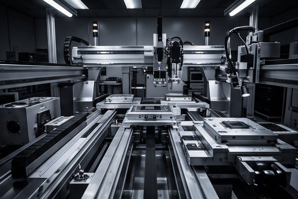
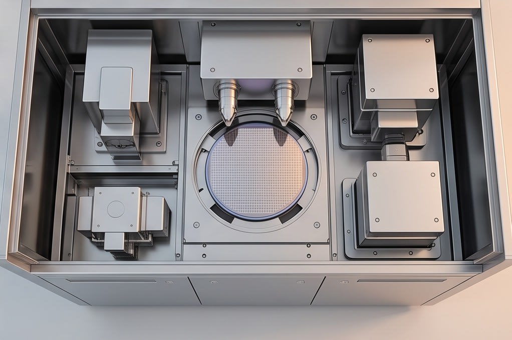
    Semiconductor process equipment equipped with a high precision stage and grinding head.

    Ultra Precision Grinding Design of the PKG Grinder

    There is a way to address this issue from the process equipment design stage. The PKG Grinder from Huvics combines a high precision stage with a diamond wheel to process various package types such as FCBGA, WLCSP, and QFN/DFN at micron level accuracy. The key is a control structure that keeps TTV variation within a defined range even during high speed processing. The TTV requirement for ultra thin wafer stacking processes is approximately 2.0 microns or less, and to meet this value reliably in a high speed grinding environment, spindle runout compensation and chuck flatness maintenance must be built into the equipment from the design stage.

    Another practical challenge in production sites is line flexibility. In many cases, the same equipment must handle both low volume high mix processes and high volume continuous production. The option to choose Full Auto A·B types or a Manual type is a design choice made to respond to this requirement, and it directly contributes to reducing setup loss during process changeovers. Speed and uniformity are usually in conflict, but in grinding equipment, they are implemented in a way that satisfies both conditions at the same time.
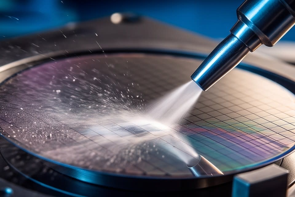
    Cleaning and drying process that removes surface residue after grinding.

    The Role of Cleaning and Drying After Grinding

    Flatness control does not end just because the grinding process is complete. Immediately after machining, grinding residue and fine particles remain on the wafer surface, and the way they are removed determines the final surface quality. This is where the choice of cleaning and drying methods becomes important.

    Comparison of Air Knife and IPA Vapor Drying

    The two drying methods mainly used in the industry are Air Knife and IPA vapor drying. Air Knife mechanically pushes liquid off the surface using a high speed gas jet, and according to research published on ResearchGate, drying within 2 seconds is possible under a speed condition of 150mm/s. In contrast, IPA vapor drying uses ultrapure isopropyl alcohol vapor to lower surface tension and guide moisture to flow away naturally without leaving marks.

    Because the two methods control processing speed and the risk of surface residue in different ways, the selection criteria vary depending on the surface characteristics of the target device and the process requirements.

    Multi Step Cleaning for Components Sensitive to Surface Contamination

    For components sensitive to surface contamination, such as camera modules, sensors, and VCM motors, a multi step cleaning approach that combines micro bubbles and water jets is becoming established.
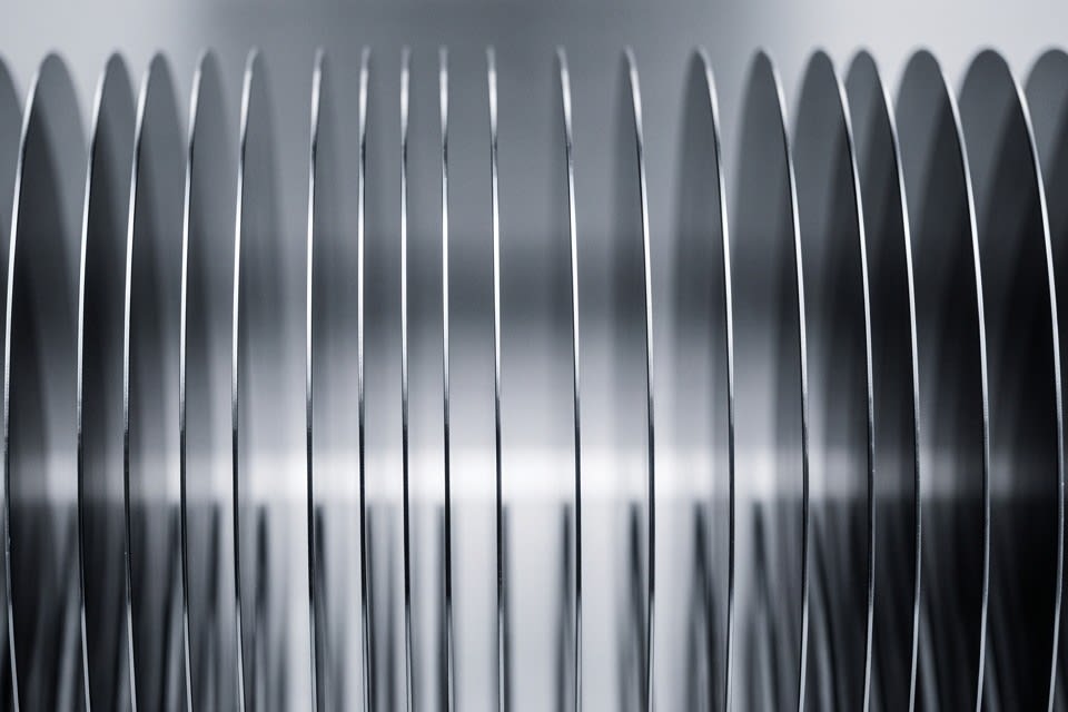
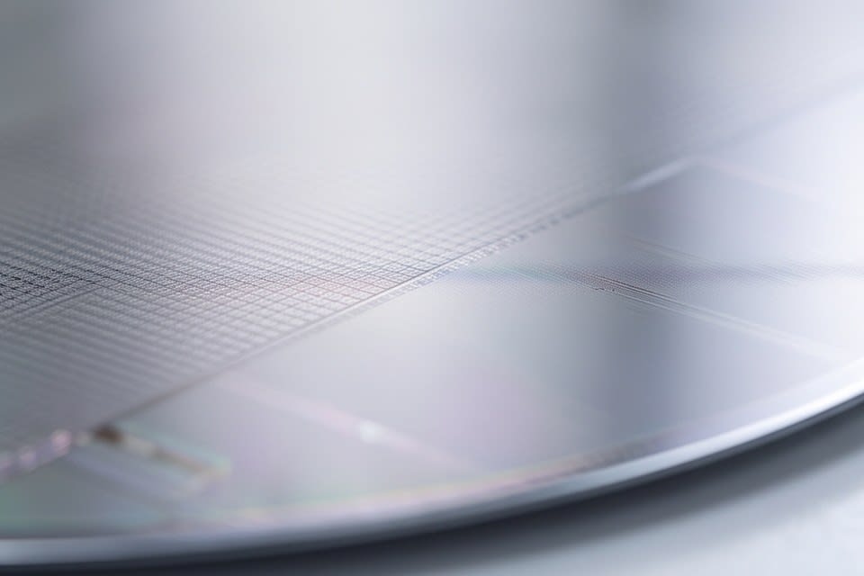
    A circular plate structure expressing the precision of the semiconductor chip stacking process.

    More than how many chips are stacked, how uniformly they are stacked determines the actual yield. From grinding precision to the selection of cleaning and drying methods, the quality of the packaging process is completed on a structure where each stage supports the next. The joke mentioned at the beginning, “stacking them is far too difficult,” turns out to describe the essence of process design quite accurately.


    Huvics is an advanced technology company that develops and manufactures automation equipment and
    production systems across the semiconductor, LED, Mobile, and Cosmetic industries.
    With top tier talent and continuous technological innovation, we support improvements in customer productivity and
    help secure quality competitiveness.

    Huvics Contact

    Phone: 031-374-8285
    Email: cdpark@huvics.com

    Contact Huvics

  • AI Semiconductor Stacked Packages: Why the Grinding Process Became the Starting Point for Yield

    AI Semiconductor Stacked Packages: Why the Grinding Process Became the Starting Point for Yield

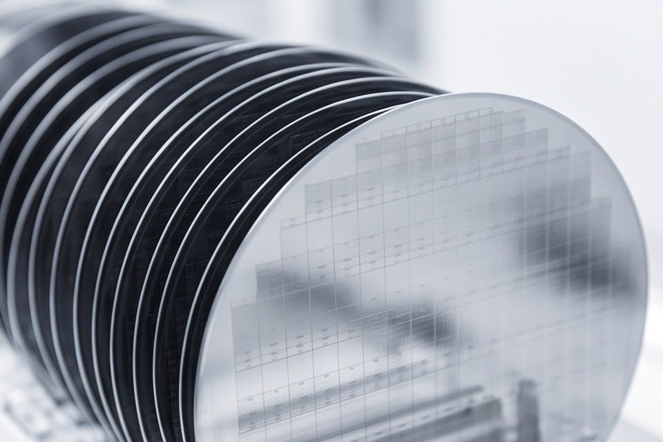
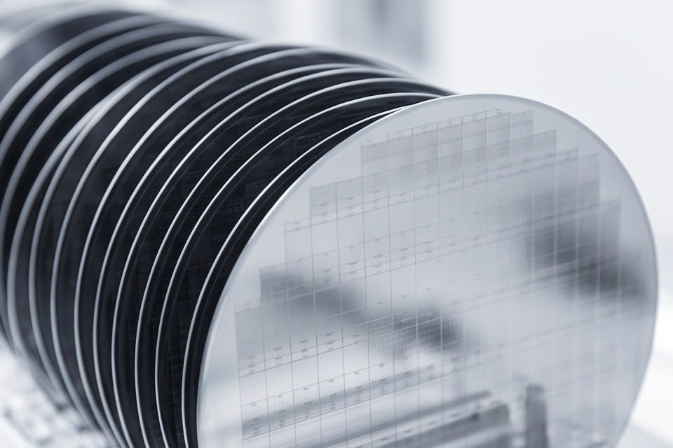
    Multiple wafers stacked vertically

    In semiconductor packaging, controlling thickness was long regarded as simply grinding materials thin enough. However, with the arrival of high-performance artificial intelligence semiconductors that stack multiple chip layers, that standard has changed completely. Simply making the material thinner is no longer enough to ensure bonding reliability in stacked structures, and minute thickness variations in each layer can accumulate and affect the performance of the entire package. Today, a completely different level of grinding technology is required, one that can secure micron-level uniformity and flatness at the same time.

    Cross section of wafers stacked vertically in multiple layers

    Why Thickness Uniformity Becomes a Prerequisite in Stacked Packages

    In stacked package structures where dozens of chips are piled vertically, thickness variation in each layer is not merely a dimensional issue. The more precisely designed the package substrate structure is, as in FCBGA(Flip Chip Ball Grid Array) or WLCSP(Wafer Level Chip Scale Package), the more the uniformity of remaining thickness after grinding becomes a prerequisite for all subsequent processes.

    In particular, WLCSP eliminates the substrate and mounts the chip directly onto the main board, so the impact of grinding precision appears immediately in electrical characteristics as the signal path becomes shorter. According to data from the United States Patent and Trademark Office(USPTO), the current target thickness for wafer backside grinding is about 300μm(microns), and it is expected to become even thinner in the 200 to 250μm range going forward. As the thickness target becomes lower, the allowable margin of error also becomes narrower, while the level of precision required in the process increases inversely. In this trend, the role of the grinding process is increasingly becoming a key variable in packaging quality.

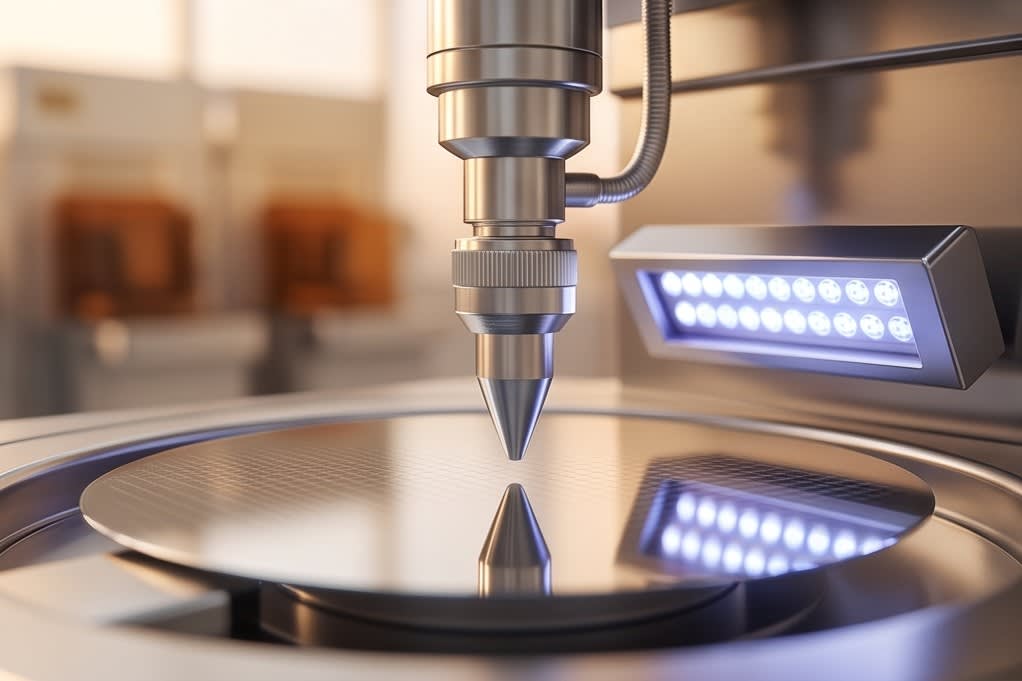
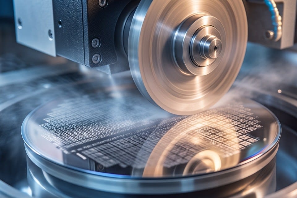
    A semiconductor wafer rotating while being precision ground by a diamond wheel

    The Two-Step Structure and Tolerance Standards of Precision Grinding

    To understand the tolerance level required by precision grinding, a sense of proportion is more important than the numbers themselves. The allowable tolerance required in grinding for semiconductor manufacturing equipment is about ±2.54μm(microns), which is only a few dozenths of the thickness of a human hair, considering that human hair is about 70 to 100μm thick.

    To reliably achieve this level of precision, commercial grinding systems operate two process stages in sequence.

    • Coarse grinding stage: Rapidly removes material at a speed of about 5μm per second.
    • Fine grinding stage: Reduces the speed to 1μm per second or less to secure surface roughness and thickness uniformity.

    Reducing speed is the core principle for increasing precision, and how precisely the transition point and conditions between the two stages are controlled is the key factor that determines final yield. Equipment configuration that combines a diamond wheel with a high-precision stage is the core hardware that reliably supports this transition process, and the completeness of equipment design is directly revealed under conditions that must satisfy both fine tolerance control and repeatable reproducibility.

    Precisely processed semiconductor packages arranged on a tray

    How PKG Grinder Responds to On-Site Conditions

    When introducing grinding equipment at an AI semiconductor packaging site, the first practical question is “which package types can it support”. In many cases, a single production line must handle multiple packages at the same time, including FCBGA, WLCSP, and QFN/DFN(Quad Flat No Lead), while the target thickness required by customers differs by product.

    Huvics PKG Grinder is designed for these on-site conditions with Full Auto A/B types and Manual type options, allowing flexible selection according to the automation level of the production line and the characteristics of the product. Processing uniformly and precisely to the thickness customers require is not simply a matter of equipment specifications. It means the equipment must allow settings that reflect actual process conditions and package structures.

    The requirement to maintain stable yield even during high-speed processes in manufacturing sites that handle ultra-precision components, such as camera modules or autonomous driving sensors, directly shows how important repeatable reproducibility and in-process consistency are for equipment. As stacked structures become more complex and target thickness becomes thinner, the range of precision that grinding equipment must handle also expands. This is where the significance of PKG Grinder in this process becomes clear.

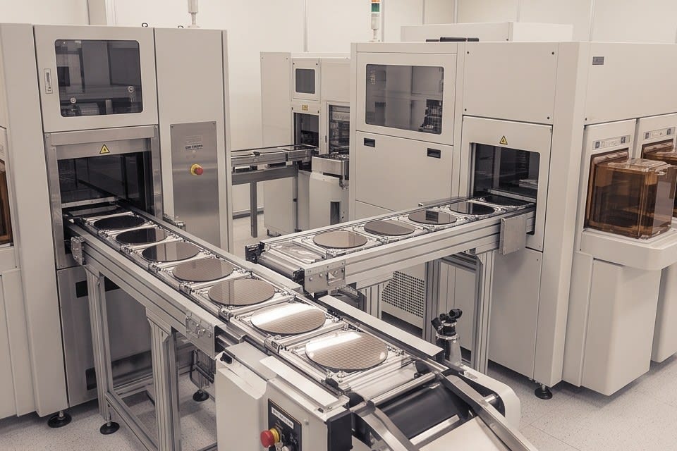
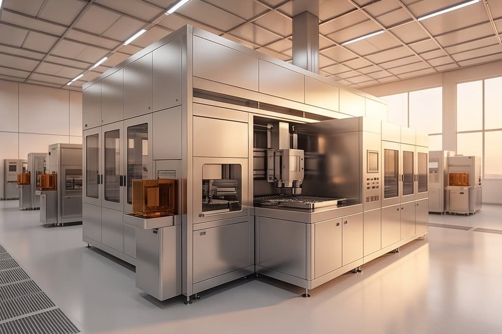
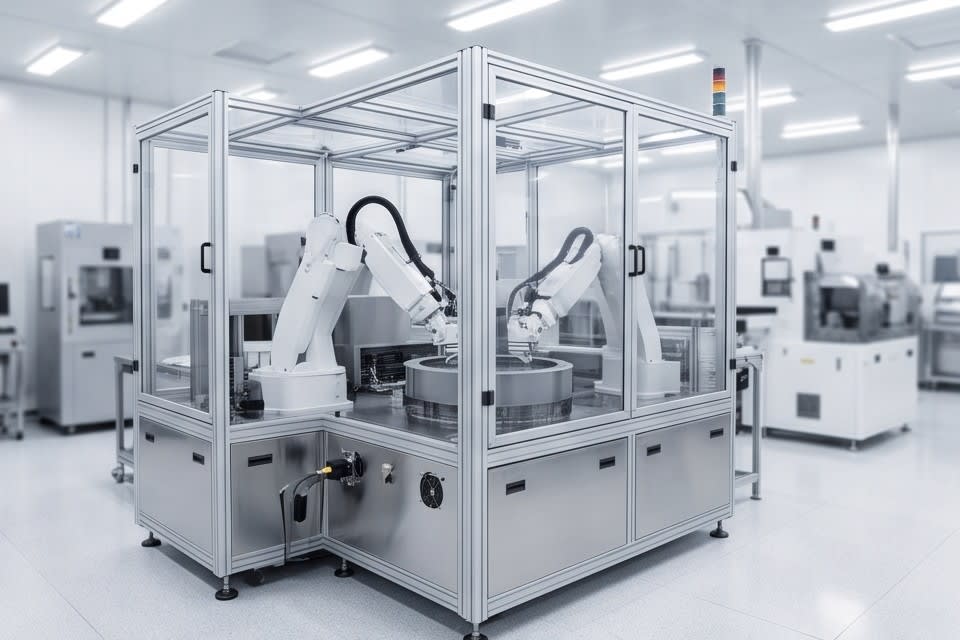
    Exterior of an automated grinding system installed in a cleanroom environment

    The complexity of stacked structures required by AI semiconductors has transformed the grinding process from a simple post-processing step into the starting point of quality. The ability to repeatedly achieve micron-level tolerances ultimately shows where the reliability and yield of the entire package are determined. As thickness targets become thinner and the number of stacked layers increases, the demand for grinding precision will continue to rise.


    Huvics is an advanced technology company that develops and manufactures automation equipment and
    production systems across the semiconductor, LED, Mobile, and Cosmetic industries.
    With top-level talent and continuous technological innovation, we support customers in improving productivity and
    securing quality competitiveness.

    Huvics Contact Information

    Phone: 031-374-8285
    Email: cdpark@huvics.com
    Huvics Inquiry

  • How Grinding Process Uniformity Determines AI Semiconductor Packaging Yield

    How Grinding Process Uniformity Determines AI Semiconductor Packaging Yield

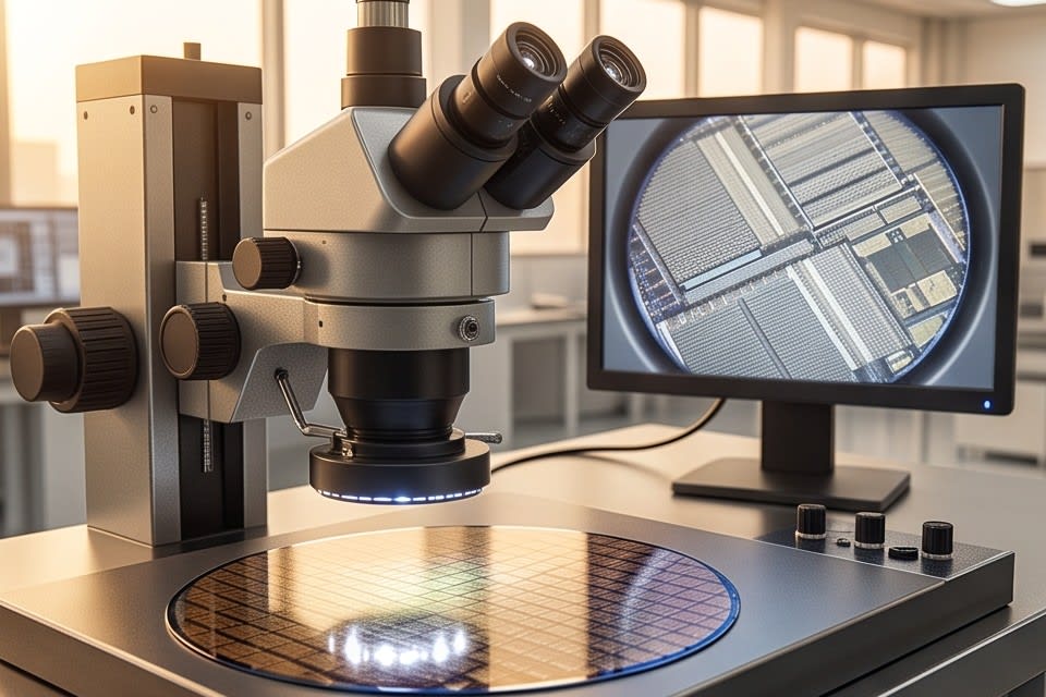
    Optical equipment inspecting fine surface conditions and uniformity in the semiconductor packaging process

    There is one fact that only some people in the semiconductor industry know. The factor that determines the performance of cutting-edge AI chips is not the design or the material, but ‘is hidden in the uniformity of the grinding process’, which is difficult to see with the naked eye. Over time, a yield gap that is difficult to close emerges between sites that understand this fact and those that do not.

    Fine structure of a vertically stacked 3D semiconductor chip cross section

    Why thickness uniformity and flatness determine yield

    In the packaging of AI semiconductors and high-performance memory semiconductors, thickness uniformity and flatness are not simple dimensional requirements. In a 3D stacked structure where chips are stacked vertically, the surface condition of each layer directly determines the bonding quality of the upper and lower layers. According to a technical report by Applied Materials, the uniformity of the wafer surface directly affects stacking yield, reliability, and electrical performance, and even slight surface variations can degrade bonding quality.

    As the number of stacked layers increases, these requirements become even stricter. According to industry discussions reported by TrendForce, the current thickness standard for HBM4, fourth-generation high-bandwidth memory, is 775 micrometers, and raising it to the 825~900 micrometer level is being considered for next-generation HBM4E and HBM5. As technology evolves toward stacking more chips higher, how precisely the flatness of each layer is controlled determines the reliability of the entire package.

    A single thickness error can distort the path of an electrical signal, and that leads to yield loss. This is why ultra-precision processing becomes a prerequisite, not an option, and standards for equipment that meets these requirements are also rising.

    Grinding equipment that uniformly processes the wafer surface through a combination of a high-precision stage and a diamond wheel

    Ultra-precision grinding technology of the PKG Grinder

    Huvics PKG Grinder is high-precision grinding equipment designed to respond to these strict standards. By combining a high-precision stage with a diamond wheel, it enables thickness processing at the micron level and can be applied to various package types, including FCBGA, flip chip ball grid array, WLCSP, wafer level chip scale package, QFN·DFN, and solar cells.

    What is highly valued on production sites is not only its high precision, but also the fact that it maintains stable quality even in high-speed processes and achieves high yield. Depending on the characteristics of the production line, users can choose from fully automated, Full Auto, A type·B type and Manual types, making it flexible for both high-mix low-volume lines and high-volume continuous production lines. For packages that require micron-level precision, the repeatability of equipment determines yield, and whether that repeatability can be maintained even under high-speed conditions is the key factor in equipment selection.

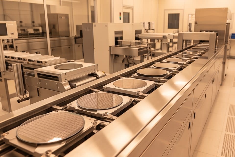
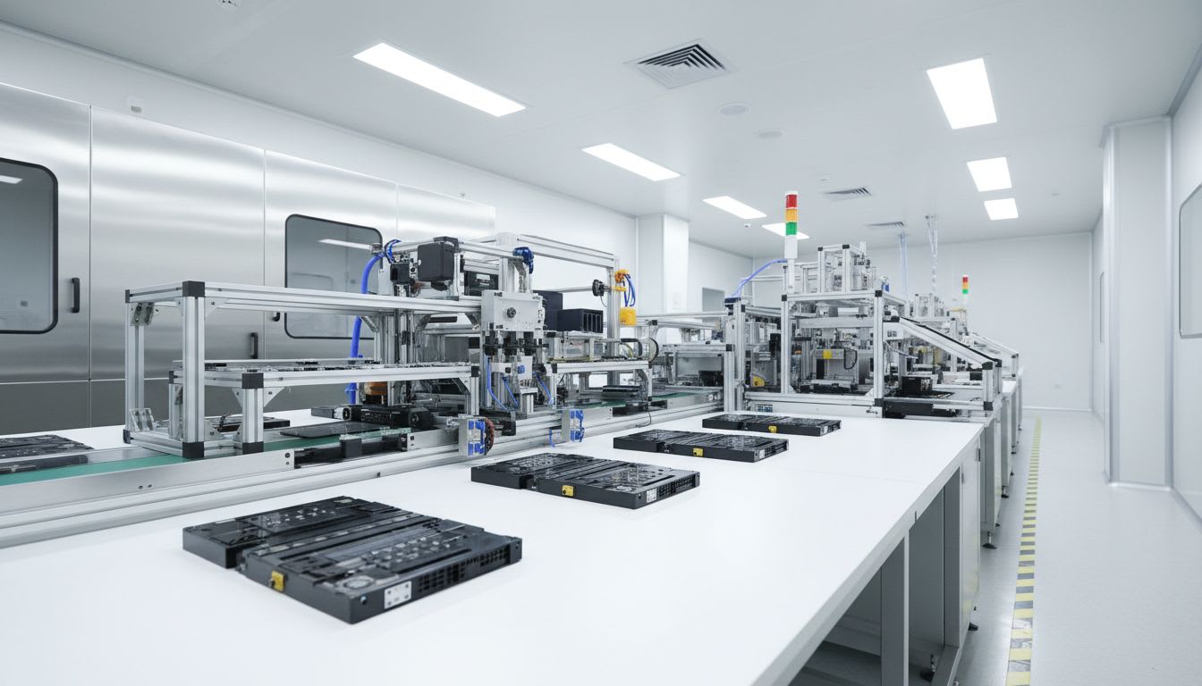
    An operator managing an automated process site through a conveyor system in a cleanroom environment

    The relationship between process automation and cost control

    On the production floor, the impact of equipment selection on the cost structure is greater than many expect. In the industry, unplanned downtime in semiconductor manufacturing lines is known to cause losses of more than 260,000 dollars per hour, and even the same repair is reported to cost 3~5 times more in an unplanned situation than when handled during scheduled maintenance. This is why equipment stability and maintenance predictability become financial decision criteria beyond simple operational convenience.

    The same logic applies to the cleaning process. A method that combines micro bubbles, water jets, and air knives in stages for cleaning various components such as camera modules, sensors, VCM motors, and trays is an approach that removes contamination particles and lowers defect rates in a single process. The laminator system also integrates everything from lamination to UV curing into one flow, reducing process steps and shortening tact time.

    The direction of integrating processes and raising the level of automation is ultimately the way to secure both predictable quality and cost control, and its significance is confirmed in the actual numbers from production sites.

    A stacked semiconductor chip with fine interconnections precisely bonded together

    The precision requirements for AI semiconductor packaging will continue to rise. In this trend, which equipment is used and how processes are configured determine not only current yield, but also the capability to handle next-generation products. The fact that a single grinding process holds the reliability of the entire package is why precision processing equipment deserves attention in this market.


    Huvics is an advanced technology company that develops and manufactures automation equipment and
    production systems across the semiconductor, LED, mobile, and cosmetics industries.
    With top talent and continuous technological innovation, we support customers in improving productivity and
    securing quality competitiveness.

    Huvics Contact

    Telephone: 031-374-8285
    Email: cdpark@huvics.com
    Huvics Inquiry

  • Why Yield Changes When You Follow the 4 Steps of the Semiconductor Cleaning and Drying Process in Order

    Why Yield Changes When You Follow the 4 Steps of the Semiconductor Cleaning and Drying Process in Order

    A systematic and clean semiconductor production line processing ultra-precision components.

    If you are in charge of designing or improving a semiconductor production line for the first time, you have probably felt uncertain when facing the cleaning process. Which cleaning method should be selected, whether drying can be handled within the same process, and how far the level of automation should go. There is an overwhelming amount of information, but without clear standards it can become even more confusing. It is natural for the cleaning process to feel difficult. From here, let us look at its structure step by step.

    A circuit board equipped with camera modules and sensors that are sensitive to microscopic contamination.

    Why Cleaning Determines Yield

    It is often said that cleaning is important in semiconductor processes, but the impact feels different when the reason is shown in numbers. According to research by CMC Northeastern, 75% of yield loss in semiconductor integrated circuit manufacturing originates from contaminants. If a single microscopic particle settles on the substrate during the exposure process, it can lead to a 5~15% yield loss per batch.

    Contaminants begin disrupting the process at sizes invisible to the eye. In ultra-precision component manufacturing sites where surface cleanliness is directly connected to performance, such as camera modules or autonomous driving sensors, this issue becomes even more sensitive. The quality standards required in the automotive electronics industry cannot be met by visual inspection alone. The understanding that the cleaning process is the starting point of yield is now widely established across the industry.

    A multi-step cleaning system where water jets and microbubbles are applied through spray nozzles.

    Structure of the 4-Step Cleaning and Drying System

    The 4-step cleaning and drying system is structured to apply microbubbles, water jets, air knives, and oven drying in sequence. Each step has a different role.

    • Microbubbles lift microscopic contaminants without physical impact on the surface.
    • Water jets push away the lifted contaminants.
    • Air knives serve as the primary drying step by removing moisture remaining on the surface.
    • Oven drying handles the final step by removing residual moisture.

    This structure processes cleaning and drying together within one system instead of separating them into different processes. The Huvics cleaner system is designed to integrate these 4 steps into a single line and apply them to cleaning various components such as camera modules, sensors, VCM motors, and trays. Both Full Auto and Manual methods can be selected, allowing the system to be configured according to the automation level and maintenance conditions of the production line.

    An organized automated production line that reduces labor time in the cleaning process.

    Practical Effects and Decision Criteria for Automation

    The difference between manual cleaning and automated cleaning is not simply a matter of speed. In a case from Alliance Manufacturing, direct cleaning labor time was reduced by about 60% after switching from a manual solvent cleaning method to an automated system. According to an analysis by Zenith Ultrasonics, ultrasonic cleaning can reduce cleaning time by 60~85% compared to traditional methods.

    What these figures mean is that the process layout within the production line changes. When the time required for the cleaning process is reduced, there is room to redesign the connection structure with the previous and following processes. However, introducing automation is not equally suitable for every site. Depending on the diversity of production items, batch size, and workforce operation method, there are environments where Manual can be more advantageous than Full Auto.

    The reason the Huvics cleaner system is configured to allow selection between the two methods is that it reflects these differences in site-specific conditions. The key to determining which method is right is to first understand the overall flow of the process.

    An automated cleaning line where robot arms and conveyors are integrated and organically connected.

    How the cleaning process is configured is ultimately connected to the question of where to begin designing the efficiency structure of the entire production line. The fact that contamination control is a key variable for yield, the possibility of integrating cleaning and drying into one process, and the flexibility to select the automation level according to the site. Only when these three factors are considered together does the direction of the line layout become clear. When what felt difficult at first begins to appear as a structure, the criteria for making decisions also become clearer little by little.


    Huvics is an advanced technology company that develops and manufactures automation equipment and
    production systems across the semiconductor, LED, Mobile, and Cosmetic industries.
    With top-tier talent and continuous technological innovation, Huvics supports customers in improving productivity and
    securing quality competitiveness.

    Huvics Contact

    Phone: 031-374-8285
    Email: cdpark@huvics.com

    Huvics Inquiry

  • Manual Inspection vs Automated Cleaning and Drying System, Where Semiconductor Yield Is Decided

    Manual Inspection vs Automated Cleaning and Drying System, Where Semiconductor Yield Is Decided

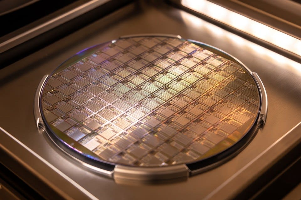
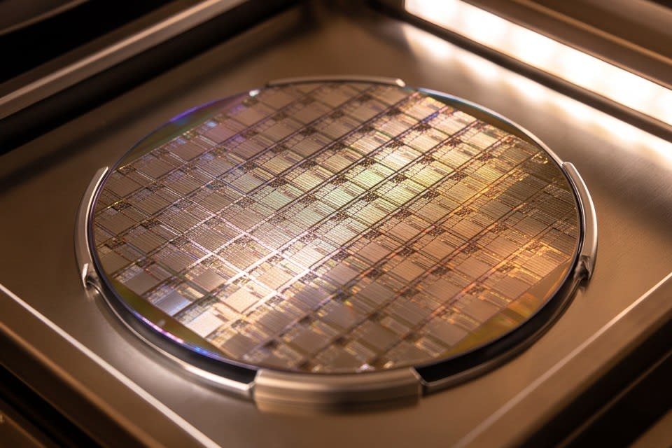
    Precisely integrated circuit patterns on a semiconductor wafer.

    There is a saying among semiconductor process engineers. “If you take cleaning lightly, you can easily lose yield.” Of course, it is hard to confirm whether anyone actually says this, but that is exactly the atmosphere on the production floor. A single speck of dust or one drop of oil can bring down an entire process that has been built with extreme precision. Cleaning may look like the final step of a process, but in reality, it is the starting line of quality.

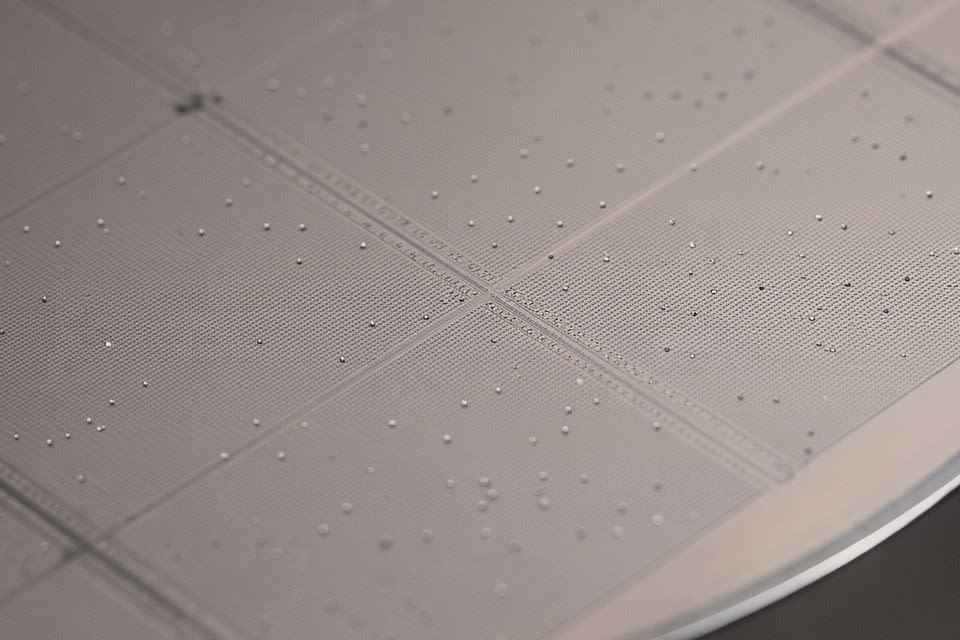
    A close up view of microscopic particles scattered across the surface of a semiconductor wafer.

    The Impact of Microscopic Contamination Particles on Yield

    In semiconductor and advanced electronic component manufacturing, microscopic contamination particles are not simple impurities. According to analysis by TSI, a single particle on a wafer can lead to failures in multiple integrated circuits and significantly reduce overall yield. What makes the issue even more demanding is size. The fact that particles as small as 0.05 micrometers can cause critical defects in semiconductor chips clearly shows that the cleaning process is not just a simple act of washing.

    It is already widely recognized in the industry that particle defects account for a significant share of all defects in high density electronics manufacturing. As ultra fine processes become standard, contamination tolerance limits become even tighter, and the technical completeness of the cleaning stage is increasingly determining the reliability of the final product.

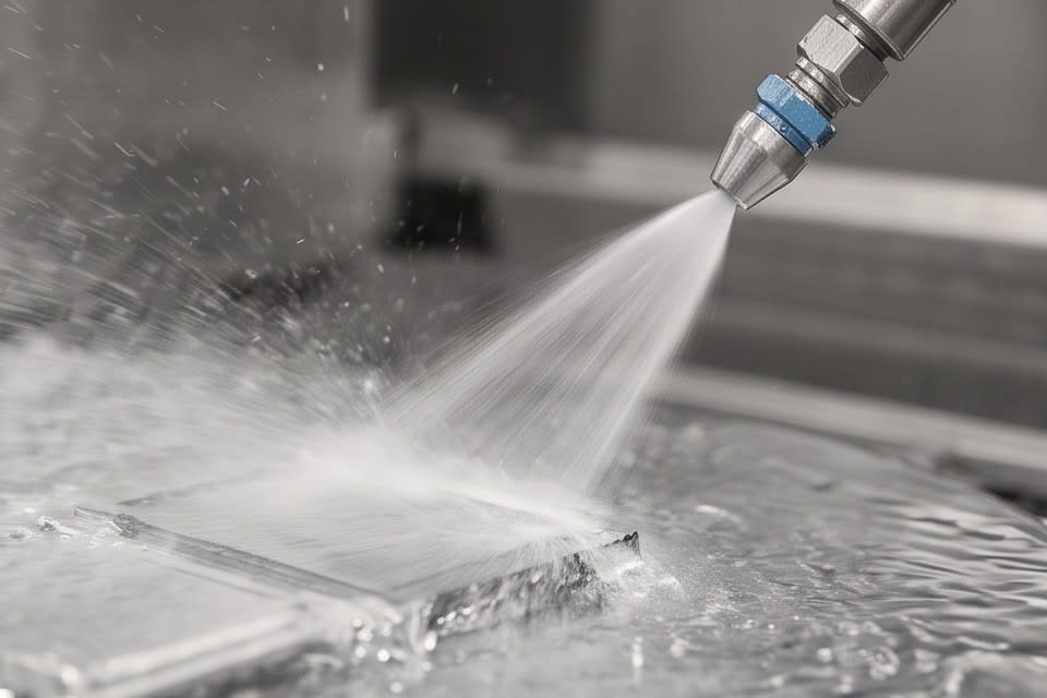
    A high pressure stream of water sprayed from a nozzle washing the surface of a component.

    Multi Stage Cleaning and Drying Technology of the Cleaner System

    The Cleaner System approaches this problem step by step. Its configuration, consisting of Micro Bubble, Water Jet, Air Knife, and Oven Dry, allows each stage to remove contamination and complete drying in a different way.

    Micro bubbles are fine bubbles with diameters ranging from 10 micrometers to several tens of micrometers. They are generated when dissolved air reaches a certain concentration and physically separate contamination particles adhered to the surface. Water Jet removes surface residues with a high pressure water flow, while Air Knife pushes away moisture with a sharp air stream to create the proper condition for the next stage. The final Oven Dry stage completely removes remaining moisture and completes the drying process.

    Depending on the product type, such as camera modules, sensors, VCM motors, and trays, a Full Auto or Manual configuration can be selected to match the conditions of the production site. It is implemented through a design method that treats cleaning and drying not as separate processes, but as one continuous flow.

    Combining Vision Inspection and Ultrasonic Dispersion Technology

    Precision is also required without compromise in the quality verification stage after cleaning. While manual inspection, even when performed by skilled operators, remains at an accuracy level of 85~90%, research published on ResearchGate shows that automated optical inspection(AOI) achieves 98~99% accuracy and processing efficiency of more than 5,000 units per hour. At the point where the human eye reaches the limits of fatigue and concentration, algorithms operate without fluctuation.

    Huvics applies this principle to MLCC and FPCB processes by combining its proprietary ultrasonic dispersion technology with vision inspection algorithms. Ultrasonic dispersion increases particle separation efficiency during the cleaning stage, and the vision inspection algorithm detects remaining defects down to a microscopic level afterward. Because the two technologies operate sequentially, the performance of one stage supports the effectiveness of the other. The key is to connect the cleaning process and the inspection process within a single quality management system, rather than treating them separately.

    Multiple wafers moving along automated equipment.

    There is something often overlooked when selecting a cleaning and drying system. It is not just the performance of the equipment, but how it connects with the entire process. No matter how precise the cleaning technology is, if it does not align with the inspection stage, defects are found too late and yield loss has already accumulated. In semiconductor and advanced component manufacturing, quality stability is not created by the completeness of a single process, but by the entire flow from cleaning to drying and inspection. How that flow is designed ultimately determines product reliability.


    Huvics is an advanced technology company that develops and manufactures automation equipment and
    production systems across the semiconductor, LED, Mobile, and Cosmetic industries.
    With top talent and continuous technological innovation, Huvics supports customers in improving productivity and
    securing quality competitiveness.

    Huvics Contact

    Phone: 031-374-8285
    Email: cdpark@huvics.com
    Huvics Inquiry

  • How the Integrated Lamination·Cleaning Process Improves Stacked Semiconductor Yield

    How the Integrated Lamination·Cleaning Process Improves Stacked Semiconductor Yield

    A semiconductor manufacturing site where wafers move along connected conveyor belts

    To reduce defect rates in semiconductor processes, many manufacturers have focused on improving the precision of individual equipment. Typical approaches include adopting more sophisticated stencils and faster inspection equipment. However, even when the performance of each piece of equipment is enhanced, contamination and alignment errors that occur during transfer between processes still hold back yield. It is now time for an integrated design perspective that connects the entire process into one continuous flow.

    A scene showing blue tape being attached to and peeled from a wafer surface

    Why tape attachment and UV curing determine stacked packaging quality

    In stacked semiconductor packaging, tape attachment and UV curing are not simply auxiliary material processes. The entire sequence from fixing chips onto the wafer to peeling them accurately after dicing depends on these two steps.

    UV curing technology creates immediate adhesion and high tensile strength the moment ultraviolet light activates the photoinitiator inside the adhesive. When ultraviolet light is applied again afterward, adhesion decreases, allowing the chip to be removed cleanly from the tape. If this precise control of adhesion and peeling is not achieved, residual adhesive may remain on the chip surface or microcracks may occur during peeling.

    Especially in ultra-fine packages with a pitch level of 0.3~0.4mm, placement alignment errors must be controlled within several tens of micrometers, and variations in curing timing and intensity lead directly to process defects. As stacked structures become more complex, requirements for thickness uniformity and flatness of each layer also increase.

    Because even slight variations that occur during the tape attachment stage are amplified later in grinding or dicing processes, the stability of the initial adhesion process becomes the baseline for overall yield. Ultimately, maintaining consistent UV exposure uniformity and adhesive strength is the key to stacked packaging quality.

    An integrated laminator system combining an expander and mounter into one unit

    How an integrated laminator structure enhances process quality

    Problems that arise when process equipment is operated separately often come not from the performance of the equipment itself, but from the sections between equipment. Every time a wafer or substrate moves from the expander to the tape mounter and then to the UV curing equipment, the possibility of foreign particle inflow and alignment deviation arises. For process managers, the parameters of each piece of equipment must be managed separately, and it is also difficult to identify at which stage a problem that occurred during transfer originated.

    As the number of transfers decreases, contamination contact points are reduced and continuity of conditions between processes is secured. For this reason, one-stop laminator structures that handle everything from expanding to UV curing within a single system are gaining attention.

    The Huvics laminator system integrates lamination, tape mounting, and UV curing into one flow to reduce quality variables that occur during transfer between processes, while its UV curing system supporting both lamp and LED methods secures adhesive strength and process stability together. With both semi-auto and manual options, it flexibly supports everything from high-mix, low-volume production to mass production lines.

    By simplifying the process, takt time is reduced, and a workflow that eliminates bottlenecks is becoming established on manufacturing floors.

    A cleaning process that removes contaminants from a wafer surface using liquid sprayed from a nozzle

    Why the cleaning process determines final yield

    The cleaning process is often regarded as a finishing step that wipes the surface after assembly is completed, but in reality, it is closer to the starting point that determines final quality stability. Contaminant particles only a few micrometers in size remaining on the semiconductor surface can cause poor electrical contact or degraded optical characteristics, which directly leads to yield loss.

    According to industry analysis, a 1% increase in yield in semiconductor manufacturing can generate an estimated additional net profit of about 150 million dollars, showing that the economic impact created by differences in cleaning efficiency is significant.

    The Huvics cleaner system uses a multi-stage cleaning method that combines micro bubbles, water jet, and air knife to remove contaminant particles from product surfaces step by step. It optimizes cleaning conditions for products with diverse shapes and materials, such as camera modules, sensors, VCM motors, and trays, and is equipped with an oven drying function to completely remove residual moisture after cleaning. Users can choose between full-auto and manual methods depending on line conditions, allowing flexible response to both process automation and maintenance.

    As particle removal efficiency increases, defect rates decrease, and the rework ratio in subsequent inspection processes is also reduced through a chain effect. Only when cleaning is complete does the entire process close, and its meaning is confirmed in the final shipment quality figures.

    Light being evenly applied over multiple wafers arranged at regular intervals

    In semiconductor processes, quality depends not on the performance of any single piece of equipment, but on how tightly each process is connected to the next. Only when the precision of tape attachment, the uniformity of UV curing, and the completeness of cleaning each perform their roles can the yield curve become stable. Reducing gaps between separated equipment and designing the process flow as one connected system is the direction that manufacturing sites need today.


    Huvics is an advanced technology company that develops and manufactures automation equipment and
    production systems across the semiconductor, LED, Mobile, and Cosmetic industries.
    With top talent and continuous technological innovation, Huvics helps customers improve productivity and
    secure quality competitiveness.

    Huvics Contact Information

    Phone: 031-374-8285
    Email: cdpark@huvics.com

    Huvics Inquiry

  • 3 Core Principles Behind How Semiconductor Cleaning Processes Affect Yield and Production Cost—How Are You Managing Them?

    3 Core Principles Behind How Semiconductor Cleaning Processes Affect Yield and Production Cost—How Are You Managing Them?

    Close-up view of a silicon substrate engraved with fine circuit patterns

    In semiconductor production lines, one point many still overlook is that more than half of defects originate from invisible microscopic contaminants. A single cleaning process determines yield, and yield directly determines unit cost. Once you understand this connection, it becomes clear why precision cleaning technology is treated as a critical variable in semiconductor manufacturing.

    Silicon wafer with precise fine circuit patterns highlighted

    Why the Cleaning Process Determines Yield and Production Cost

    In semiconductor manufacturing, cleaning is not a finishing process but the starting point of quality. A single microscopic particle left on the chip surface can cause a circuit short or damage an insulating layer, turning the entire chip into a defective product. As this problem accumulates, yield drops, and as yield drops, the cost required to produce each chip rises.

    According to analysis by KeyLink, manufacturing yield loss caused by inefficient cleaning reaches 5~15%, while the introduction of precision cleaning equipment has been shown to reduce defect-related yield loss by 8~12%. When these loss rates are viewed numerically, it becomes clear that the precision of the cleaning process is directly tied to cost competitiveness.

    As chip integration increases, the allowable size of contaminant particles becomes smaller, and cleaning requirements become more demanding. As process nodes become finer, the cleaning frequency itself also increases. Some reports show that advanced process nodes require more than 30% more cleaning steps than legacy nodes. Ultimately, the precision and stability of cleaning technology are key factors that shape the overall production cost structure.

    Numerous microbubbles gathered in liquid

    How Multi-Step Cleaning Technology Improves Microscopic Contaminant Removal Efficiency

    Microbubbles generate bubbles measuring several tens of micrometers in water and physically separate nanoparticles adhered to surfaces. The shock waves generated when the bubbles collapse, known as cavitation, instantaneously create jet speeds of up to 1,096 m/s. An MDPI study confirmed that microbubbles remove nanoparticles from silicon substrates with 90% efficiency without damaging the substrate structure.

    Residual contaminants that are difficult to remove with microbubbles alone are then washed away by a water jet using high-pressure water flow. In the next stage, an air knife removes surface moisture and remaining particles with a sharp stream of air. When these three technologies are applied in sequence, each following stage compensates for the limitations of the previous one.

    Components requiring optical precision, such as camera modules and autonomous driving sensors, require ISO Class 5 cleanliness at the point of optical system integration, and it is difficult to meet this standard consistently with a single cleaning method. Huvics’ 4-step cleaning and drying system addresses these requirements by arranging microbubble, water jet, and air knife processes sequentially, enabling the removal of microscopic contaminants from the surfaces of ultra-precision components such as camera modules and autonomous driving sensors.

    Heated processing oven equipment receiving parts through a conveyor belt

    How Integrated Cleaning and Drying Design Meets Automotive Electronics Quality Standards

    The automotive electronics industry requires strict quality standards across the entire manufacturing environment. The IATF 16949 standard requires temperature, humidity, and contamination levels in manufacturing facilities to be maintained below specified limits, and this concept also includes the management of residual moisture after cleaning. Even if cleaning is performed with high precision, any moisture remaining in the drying stage can lead to corrosion or electrical failure. For this reason, cleaning and drying should be designed not as separate processes but as one continuous process.

    Huvics’ cleaner system uses a built-in oven drying function to handle everything from cleaning to drying within a single piece of equipment. If the process is not separated, recontamination during transfer can be avoided, and if separate drying equipment is not operated, process time and equipment costs are reduced accordingly. This batch processing structure reduces both types of loss at the same time.

    As the defect rate decreases, the number of discarded parts falls, and rework costs are also reduced. As precision requirements for semiconductors and automotive electronics components continue to rise, process designs that integrate cleaning and drying are becoming a key tool for managing production costs.

    Large manufacturing equipment installed inside a cleanroom under strict management standards

    The view that cleaning is merely a procedure for maintaining cleanliness became outdated long ago. Protecting yield means protecting cost, and the fact that this begins with the cleaning stage becomes even clearer as semiconductor processes become finer. A process design that extends from microbubbles to oven drying is the result of implementing this logic directly into the equipment structure.


    Huvics is an advanced technology company that develops and manufactures automation equipment and
    production systems across the semiconductor, LED, Mobile, and Cosmetic industries.
    With outstanding talent and continuous technological innovation, we support customers in improving productivity and
    securing quality competitiveness.

    Huvics Contact Information

    Tel: 031-374-8285
    Email: cdpark@huvics.com
    Huvics Inquiry

  • Precision Cleaning and Process Automation Solutions That Determine Semiconductor Wafer Yield: Analysis of Huvics Technology

    Precision Cleaning and Process Automation Solutions That Determine Semiconductor Wafer Yield: Analysis of Huvics Technology

    Huvics

    In semiconductor manufacturing, even a microscopic residue invisible to the eye can become the trigger for a major defect. Today, as nanoscale precision processes have become standard, the cleanliness of the wafer surface is more than just one step in the process. It is a key indicator that determines the final product yield. Because such micro contamination directly leads to significant cost losses for companies, thorough and flawless surface management has now become a strategic necessity rather than an option.

    Based in Osan, Gyeonggi-do, Huvics is a group of specialists that has transformed deep challenges from the field into technical solutions, from semiconductor tape bonding processes to tray cleaning technology. Let us take a closer look at the core of the innovative process design Huvics offers for your journey to maximize production yield through precision cleaning and process automation.

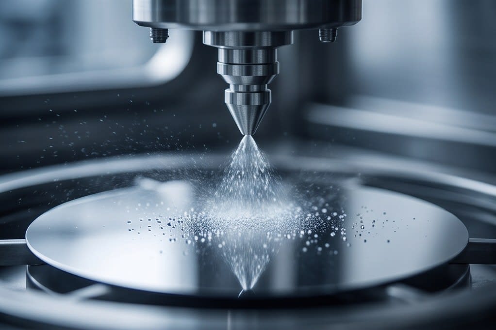
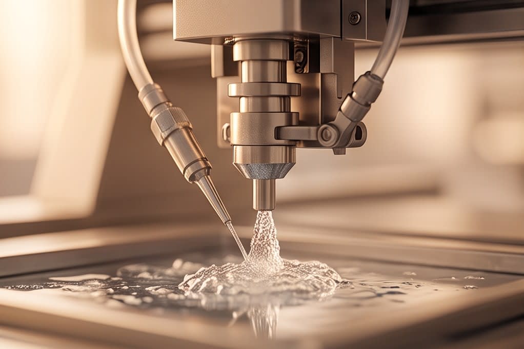
    Cleaning technology with an ultra-precision nozzle

    The Core of Semiconductor Processes, Precision Cleaning Technology

    The Impact of Micro Contamination on Yield

    In semiconductor manufacturing processes, the cleanliness of the wafer surface is a key indicator that determines the final product yield. In the modern semiconductor ecosystem, where nanoscale micro processes have become routine, even a tiny residue invisible to the eye can disrupt the pattern of fine circuits and become a critical variable that produces defective products in large quantities. Defects caused by this micro contamination directly lead to enormous cost losses for companies and ultimately weaken price competitiveness in the market.

    Huvics’ Technical Solution

    Huvics deeply understands these on-site concerns and provides the following technical solutions.

    • Solving challenging defect issues in semiconductor tape bonding processes
    • Overcoming technical difficulties encountered in tray cleaning processes
    • Responding based on extensive hands-on experience accumulated in the field

    We go beyond simply providing cleaning and support automation and simplification design across the entire manufacturing process of our customers. Through this, companies can significantly reduce unnecessary operating costs while maximizing consistency and stability in process quality. Precision cleaning technology ultimately lowers defect rates, optimizes equipment uptime, and improves overall productivity.

    With Huvics, which continues to build unmatched technological capabilities in precision cleaning and automation equipment through constant research and development, experience the highest production yield your semiconductor process can achieve.

    Site-Customized Process Redesign

    Solving Technical Challenges and Optimizing Processes

    The solutions provided by Huvics go beyond the step of simply removing contamination. They focus on fundamentally solving technical challenges in manufacturing sites and redesigning process workflows. In particular, Huvics presents site-customized response strategies by dramatically improving micro defect issues in the tape bonding process, a chronic problem in the semiconductor industry, and overcoming the physical limitations of tray cleaning technology. The many variables encountered in the field are difficult to solve with a fragmented approach.

    Sustainable Innovation and Automation Integration

    Based on years of accumulated field data, Huvics builds the most efficient precision cleaning process and tightly integrates it with automation systems. By introducing precise process automation and process simplification, we reduce the burden of chronic operating costs faced by companies while also practicing sustainable innovation that maximizes process quality stability.

    Our proven technological capabilities, developed through close collaboration with leading global companies, have become the most powerful core driver for increasing production yield in increasingly sophisticated micro process environments. When the invisible obstacles that hinder process efficiency are removed one by one through the professional perspective of Huvics, your manufacturing competitiveness will finally reach results with a higher level of perfection.

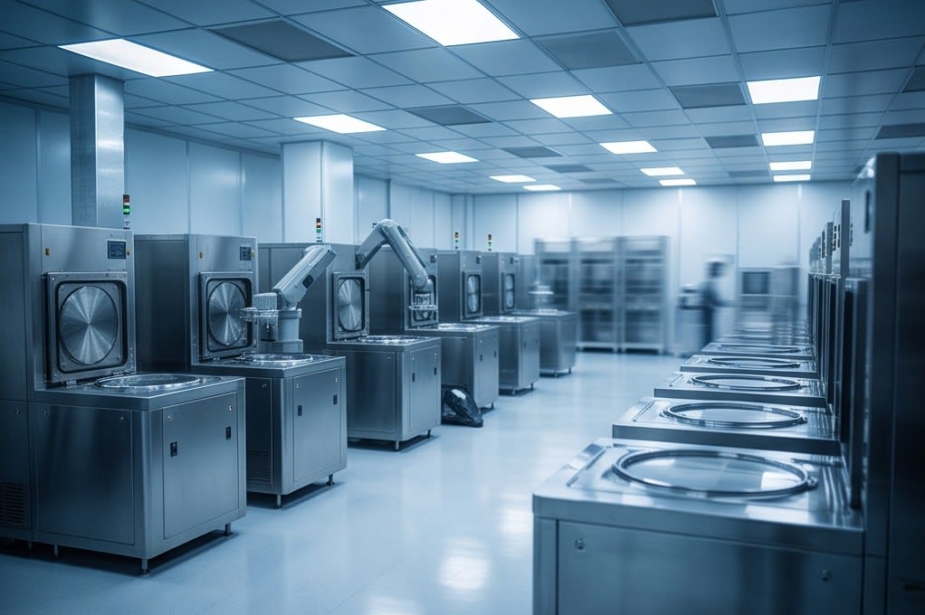
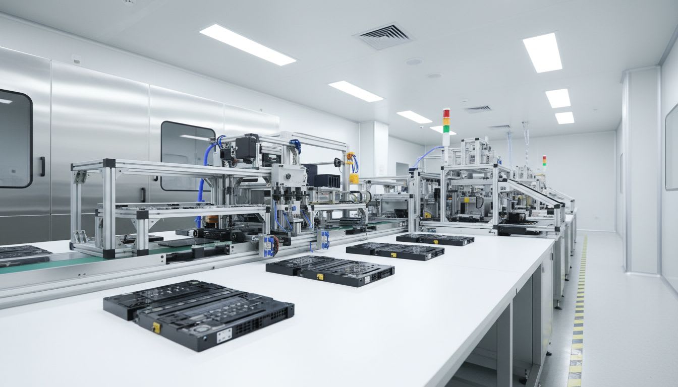
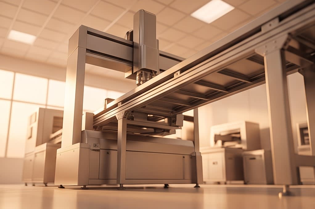
    Overview of automated equipment inside a cleanroom

    System-Based Automation Solutions

    Automation Systems for Quality Assurance

    Productivity in semiconductor manufacturing ultimately depends on how effectively invisible contamination is controlled. However, as processes become more complex, there are limits to direct human management. Huvics is advancing system-based automation solutions to address these limitations. Precision cleaning equipment is not simply a machine that wipes products clean. It is a quality assurance system that helps maintain consistent cleanliness from the beginning to the end of the process. Huvics technology, which blocks difficult contamination factors such as tape residue and fine particles at the source, is installed at key points across semiconductor production lines to continuously monitor potential threats.

    Improving Productivity and Preventing Human Error

    Reducing defect rates in the field is not simply about preventing losses. It is about increasing the mass production share of high-value-added products. Huvics diagnoses inefficient manual processes that customers struggle with and replaces them with the latest automation equipment, minimizing the room for human intervention. This improves the work environment, prevents human error, and dramatically enhances process efficiency. Huvics solutions, which integrate technical know-how accumulated in the field, solve the practical challenges customers face and help them secure manufacturing competitiveness at the next higher level.

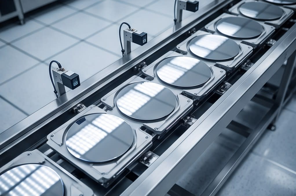
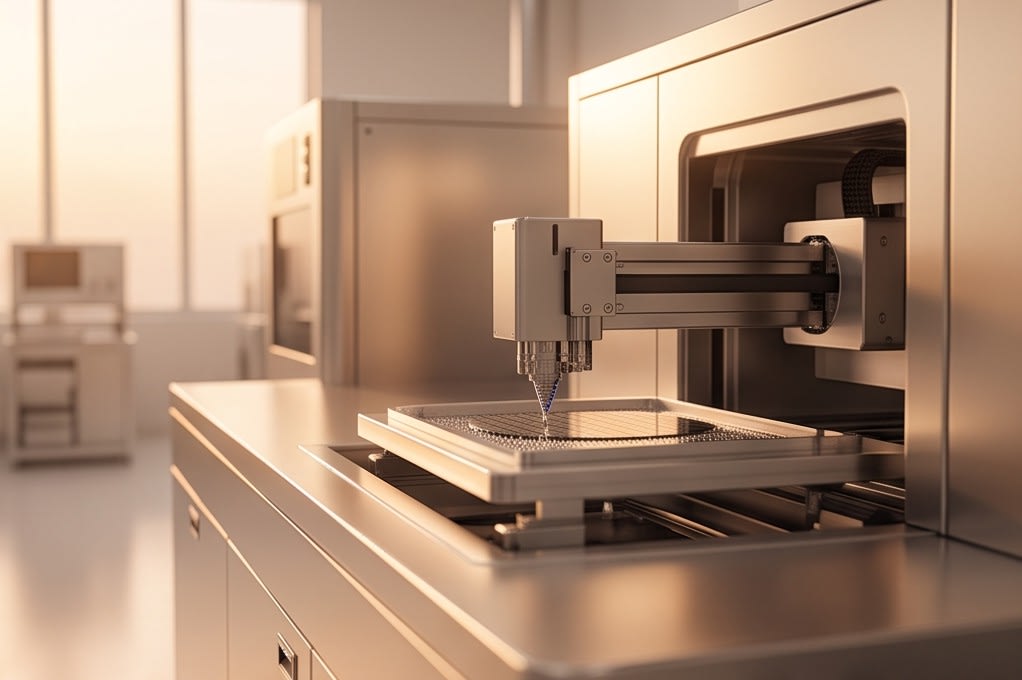
    Efficient wafer process flow

    Huvics Technology Portfolio and Future Value

    Business Success Through Customized System Implementation

    The broad technology portfolio held by Huvics is the most powerful tool for actively responding to the demanding requirements of the rapidly changing semiconductor market. Based in Osan, Gyeonggi-do, we continue to invest in research and development while advancing our technological capabilities in precision cleaning and automation equipment. On this foundation, we accurately diagnose inefficiencies in the complex manufacturing processes faced by customers and build customized systems that boldly reduce unnecessary steps, thereby substantially driving the business success of our partners. Maintaining stable quality standards amid a rapidly changing market environment is more important than anything else, and Huvics aims to be your trusted supporter at the center of creating those standards.

    Partnership for Process Innovation

    Beyond simply improving existing problems, an innovative approach that changes the paradigm of the process presents higher quality standards in the next generation semiconductor industry while also becoming a solid foundation for sustainable growth. Accumulated technological expertise in precision cleaning and deep understanding of field automation are the distinctive competitiveness of Huvics. We will provide full technical support so that your company can go beyond simple cleaning, enhance the perfection of the entire process, and achieve overwhelming production yield in the market. Through the precise technology and sincere partnership of Huvics, complete your process innovation and create future value together through higher production yield.

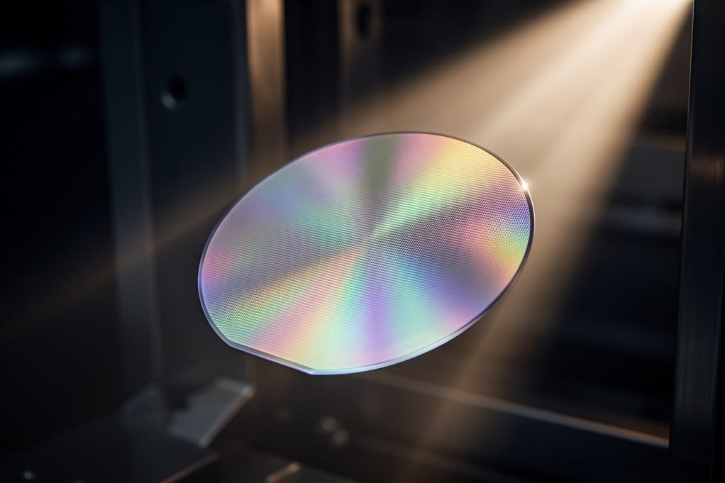
    Final quality of a defect-free wafer

    In semiconductor manufacturing, invisible micro contamination becomes a decisive variable that determines corporate competitiveness. Because cleanliness that may seem minor creates the major result known as yield, process perfection is now completed through collaboration with a partner that has technical insight.

    Based on precision cleaning technology and process automation solutions that fundamentally solve complex on-site challenges, Huvics will help your company surpass the limits of production yield and take the lead in the market. Removing invisible obstacles and innovating the process paradigm. Now, add overwhelming growth momentum to your business through the professional perspective of Huvics.


    Huvics is an advanced technology company that develops and manufactures automation equipment and
    production systems across the semiconductor, LED, Mobile, and Cosmetic industries.
    With top talent and continuous technological innovation, we support customers in improving productivity and
    securing quality competitiveness.

    Huvics Contact Information

    Phone: 031-374-8285
    Email: cdpark@huvics.com
    Contact Huvics

  • The Value of Precision Cleaning in Semiconductor Yield and the Process Innovation Strategy of the Huvics One Stop Laminator

    The Value of Precision Cleaning in Semiconductor Yield and the Process Innovation Strategy of the Huvics One Stop Laminator

    Huvics

    An industry saying states that the success or failure of semiconductor manufacturing is determined not at the beginning of a massive process, but by the level of cleanliness at the final stage. Today, that message carries even greater weight. At a time when even invisible microscopic contamination can undermine the reliability of an entire product, precision cleaning has become the final safeguard that determines production yield, going far beyond a simple auxiliary measure.

    To block unnecessary exposure within complex assembly lines and reach the highest level of manufacturing efficiency, we will explore how the process integration strategy presented by the Huvics one stop laminator system can resolve chronic bottlenecks in semiconductor manufacturing sites and maximize competitiveness.

    Integrated Laminator Solution by Huvics

    The Importance of Precision Cleaning in Determining Semiconductor Yield

    Core Value in Back End Processes

    The semiconductor manufacturing process is often described as a continuous series of fine processes, but in reality, the back end stage at the peak of that process is the most sensitive section that determines yield. Just before a wafer fully takes shape as a chip, the introduction of even a single microscopic contaminant can cause critical damage to the reliability of the entire product.

    For this reason, today precision cleaning systems have become a core process that fundamentally blocks defect factors and guarantees final product quality, rather than merely serving as an auxiliary method for removing foreign substances. In increasingly complex and sophisticated semiconductor structures, it is no exaggeration to say that cleanliness in the final stage is the last line of defense for measuring product completeness.

    Strengthening Production Efficiency and Competitiveness

    In particular, at sites where advanced equipment such as the Huvics one stop laminator is introduced, precision cleaning acts as a solution that removes chronic bottlenecks in the manufacturing process. This process goes beyond maintaining cleanliness and becomes a pivotal point that makes the entire production line flow more flexibly and dramatically improves final yield.

    Only chips completed in the cleanest possible state can meet the strict requirements of the market, and this precision cleaning strategy becomes the most reliable foundation for maintaining manufacturing competitiveness in the rapidly changing global semiconductor market.

    Core of Precision Cleaning and Curing Processes

    Technological Innovation of the Huvics One Stop Laminator

    Perfect Control of Potential Risk Factors

    The reason the Huvics precision cleaning system receives outstanding evaluations in the field is that it goes beyond the technical level of removing visible foreign substances. Inside the manufacturing environment, microscopic defect factors that are difficult to detect with the naked eye are constantly present, and the Huvics system detects these potential risk factors in advance and prevents them before they occur, ensuring product quality uniformity at a level close to perfection.

    The core technologies implemented by Huvics in the latest semiconductor assembly lines are as follows.

    • Improving process efficiency by applying an LED based UV curing process
    • Operating the precision cleaning process and UV curing stage in an organically integrated manner

    Process Efficiency Through Integrated Equipment

    In the past, each process was separated, resulting in frequent product movement, and the gaps and unnecessary exposure generated during that movement often caused takt time delays and potential contamination. However, Huvics has overcome these physical limitations by processing everything from tape mounting to expander operation and precise UV curing within a single piece of equipment.

    This integrated method, which controls residues in real time and achieves optimal adhesion strength, strengthens product durability while minimizing unnecessary movement, thereby maximizing process stability. From the producer perspective, it provides a powerful tool to minimize the probability of defects even within complex assembly stages, which directly leads to a dramatic improvement in overall production efficiency.

    Huvics is proving directly in the field that precision cleaning is a core strategic asset that supports the stability of the entire manufacturing process, going beyond simple cleanliness maintenance.

    Precise Design of the Huvics System

    A Strategic Choice for Manufacturing Innovation

    Ultimately, the competitiveness of semiconductor manufacturing depends not on the act of cleaning chips itself, but on how perfectly invisible uncertainty can be controlled. True manufacturing innovation begins only when precision cleaning is redefined from a simple maintenance concept into a strategic asset that integrates the process flow and secures quality uniformity.

    As proven by the integrated equipment of Huvics, the choice to transform process complexity into efficient simplicity will become the most powerful weapon for protecting irreplaceable quality value in a rapidly changing market. Now is the time to remove the invisible contamination factors hidden in your production line and experience a higher level of yield completeness.


    Huvics is an advanced technology company that develops and manufactures automation equipment and
    production systems across the semiconductor, LED, Mobile, and Cosmetic industries.
    With top talent and continuous technological innovation, we support customers in improving productivity and
    securing quality competitiveness.

    Huvics Contact Information

    Phone: 031-374-8285
    Email: cdpark@huvics.com

    Huvics Inquiry

  • Huvics 4-Step Precision Process that Maximizes Process Efficiency: Site-Specific Solution Strategy

    Huvics 4-Step Precision Process that Maximizes Process Efficiency: Site-Specific Solution Strategy

    Huvics

    In the fierce competition of semiconductor manufacturing sites, you know better than anyone that even a 1 percent difference in yield can determine the success or failure of a company. In particular, subtle defects in the tape adhesion process or recurring tray cleaning issues often remain unresolved challenges for site managers. Can we truly control these invisible variables completely and free ourselves from the technical hurdles we face every day? Huvics goes beyond simply supplying equipment, thoroughly analyzing the unique physical environment of each site and presenting precise answers that maximize process potential. From here, let us explore those answers through the unique 4-step precision process from Huvics, which transforms site complexity into exceptional efficiency.

    Initial diagnosis process of Huvics

    Stage 1: Site-Specific Initial Diagnosis

    Analysis of Process Variables and Root Causes

    Semiconductor manufacturing sites are a world of precision where not even the slightest error is allowed. In particular, subtle defects that occur in the tape adhesion process or the challenges of repetitive tray cleaning are often considered major technical bottlenecks that hinder production efficiency. Huvics does not try to solve these site concerns merely by supplying standardized equipment.

    We focus on the fact that every customer manufacturing line has different physical characteristics and environments. Therefore, from the initial diagnosis stage, we thoroughly analyze invisible variables within the process and the root causes of problems. This precise diagnosis becomes the logical foundation that allows the customized solution to be implemented in the most complete way.

    The First Step in a Strategic Partnership

    From precision cleaning systems to advanced automation equipment, every process designed by Huvics is the first step in a strategic partnership that helps customer production lines achieve the highest efficiency. The initial diagnosis we perform goes beyond simply identifying problems. It is like fastening the first button to bring out the full potential of the process.

    Precision cleaning solution technology

    Stage 2: Differentiated Customized Design and Implementation

    Optimal Engineering Based on Data

    Once the full-scale design stage begins, the differentiated customized engineering of Huvics comes into play. We do not simply place existing equipment on site. Instead, we conduct an optimal design process that closely reflects the extensive site data and unique process characteristics of each customer. This process is a key strategy for directly overcoming the technical challenges within the manufacturing line.

    Productivity Improvement Through Integrated Solutions

    After the design is completed, a 3-step implementation process is carried out to successfully settle precision cleaning systems and automation equipment on site. In this process, the technology of Huvics goes beyond the physical installation of equipment and functions as an integrated solution that designs the organic flow of the entire manufacturing process.

    As a result, these customized integrated solutions minimize unnecessary downtime in manufacturing lines and dramatically improve yield. Through this, companies leading the global IT and automotive electronics industries can secure a solid technical foundation that gives them a commanding advantage in the changing future technology competition environment. Customized design is the surest key to turning site complexity into simplicity.

    Customized design and implementation stage

    Stage 3: Process Stabilization and Real-Time Monitoring

    Continuous Process Tuning and Quality Maintenance

    The final stage after equipment introduction, process stabilization, is the area where Huvics places the greatest focus. No matter how advanced the technology of the equipment is, it is difficult to expect production efficiency if it cannot be fully integrated into the actual manufacturing line. Huvics continuously performs real-time data monitoring and detailed process tuning so that the installed equipment can maintain consistent high quality on site.

    The Role of a Smart Process Partner

    In this process, the equipment goes beyond simple hardware and becomes a smart partner that operates organically within the overall process flow while preventing potential bottlenecks in advance. As a result, this precise stabilization strategy from Huvics becomes a key driving force that helps customers minimize unexpected defects and secure unwavering production competitiveness.

    We make equipment more than machines that simply stand still. We enable it to breathe with the constantly evolving flow of the process. Ultimately, our goal is to become a reliable and sustainable process partner that helps customers maintain the highest productivity in any situation and secure the most dependable technological advantage.

    Precision control and defect minimization

    Stage 4: Future-Oriented Technology Partnership

    Continuous Technical Support and Innovation

    The journey of Huvics does not stop at installing and stabilizing equipment. We provide continuous technical support and future-oriented partnerships so that customer manufacturing lines can maintain optimal performance even in a changing technological environment over time. Manufacturing sites are becoming increasingly advanced, and the challenges that follow are also evolving rapidly.

    The Future of Sustainable Manufacturing

    Huvics anticipates the new technical challenges customers will face and works together to develop strategic solutions that enhance competitiveness across the entire process, beyond the equipment we supply. Through this partnership, customers experience innovation that leads future markets, going beyond the simple introduction of equipment.

    The ultimate goal of Huvics is to become a dependable technology hub that helps customers build a stable production system that remains solid at any technological turning point and become leaders who drive industrial innovation. This 4-step precision process we propose is more than a technology that improves process efficiency. It is a firm commitment to shaping the future of sustainable manufacturing together with our customers.

    Sustainable process partnership

    Conclusion

    The success or failure of semiconductor manufacturing ultimately depends on how precisely invisible errors are controlled. Going beyond simply replacing equipment, the 4-step process from Huvics analyzes complex variables on site one by one and designs an integrated flow. It is the most reliable strategic move a company can make in the ever-changing competition of future technology.

    Just as the precision we pursue becomes a powerful asset that increases customer productivity, Huvics will stay by your side as a partner that overcomes process limitations and realizes unmatched yield. The technical challenge your manufacturing line faces today may very well be the most important turning point for a new leap forward.


    Huvics is an advanced technology company that develops and manufactures automation equipment and
    production systems across the semiconductor, LED, mobile, and cosmetics industries.
    With outstanding talent and continuous technological innovation, we support customer productivity improvement and
    quality competitiveness.

    Huvics Contact Information

    Phone: 031-374-8285
    Email: cdpark@huvics.com

    Huvics Inquiry