In semiconductor production lines, one point many still overlook is that more than half of defects originate from invisible microscopic contaminants. A single cleaning process determines yield, and yield directly determines unit cost. Once you understand this connection, it becomes clear why precision cleaning technology is treated as a critical variable in semiconductor manufacturing.

Why the Cleaning Process Determines Yield and Production Cost
In semiconductor manufacturing, cleaning is not a finishing process but the starting point of quality. A single microscopic particle left on the chip surface can cause a circuit short or damage an insulating layer, turning the entire chip into a defective product. As this problem accumulates, yield drops, and as yield drops, the cost required to produce each chip rises.
According to analysis by KeyLink, manufacturing yield loss caused by inefficient cleaning reaches 5~15%, while the introduction of precision cleaning equipment has been shown to reduce defect-related yield loss by 8~12%. When these loss rates are viewed numerically, it becomes clear that the precision of the cleaning process is directly tied to cost competitiveness.
As chip integration increases, the allowable size of contaminant particles becomes smaller, and cleaning requirements become more demanding. As process nodes become finer, the cleaning frequency itself also increases. Some reports show that advanced process nodes require more than 30% more cleaning steps than legacy nodes. Ultimately, the precision and stability of cleaning technology are key factors that shape the overall production cost structure.

How Multi-Step Cleaning Technology Improves Microscopic Contaminant Removal Efficiency
Microbubbles generate bubbles measuring several tens of micrometers in water and physically separate nanoparticles adhered to surfaces. The shock waves generated when the bubbles collapse, known as cavitation, instantaneously create jet speeds of up to 1,096 m/s. An MDPI study confirmed that microbubbles remove nanoparticles from silicon substrates with 90% efficiency without damaging the substrate structure.
Residual contaminants that are difficult to remove with microbubbles alone are then washed away by a water jet using high-pressure water flow. In the next stage, an air knife removes surface moisture and remaining particles with a sharp stream of air. When these three technologies are applied in sequence, each following stage compensates for the limitations of the previous one.
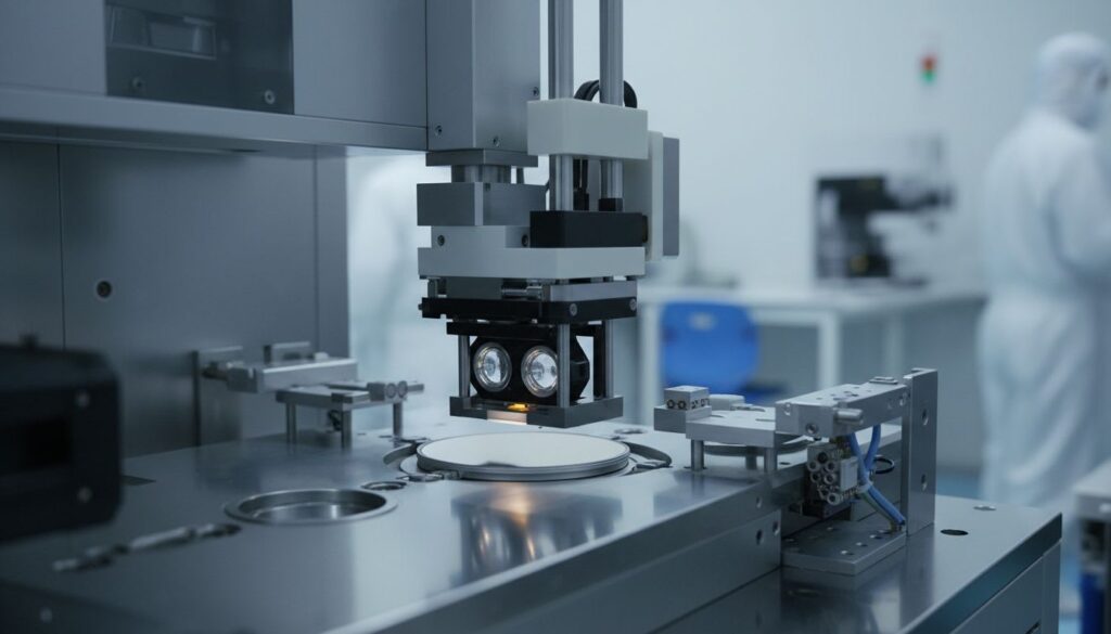
Components requiring optical precision, such as camera modules and autonomous driving sensors, require ISO Class 5 cleanliness at the point of optical system integration, and it is difficult to meet this standard consistently with a single cleaning method. Huvics’ 4-step cleaning and drying system addresses these requirements by arranging microbubble, water jet, and air knife processes sequentially, enabling the removal of microscopic contaminants from the surfaces of ultra-precision components such as camera modules and autonomous driving sensors.

How Integrated Cleaning and Drying Design Meets Automotive Electronics Quality Standards
The automotive electronics industry requires strict quality standards across the entire manufacturing environment. The IATF 16949 standard requires temperature, humidity, and contamination levels in manufacturing facilities to be maintained below specified limits, and this concept also includes the management of residual moisture after cleaning. Even if cleaning is performed with high precision, any moisture remaining in the drying stage can lead to corrosion or electrical failure. For this reason, cleaning and drying should be designed not as separate processes but as one continuous process.
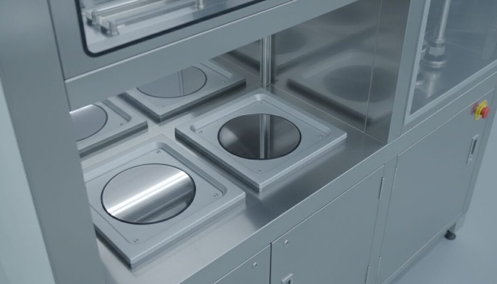
Huvics’ cleaner system uses a built-in oven drying function to handle everything from cleaning to drying within a single piece of equipment. If the process is not separated, recontamination during transfer can be avoided, and if separate drying equipment is not operated, process time and equipment costs are reduced accordingly. This batch processing structure reduces both types of loss at the same time.
As the defect rate decreases, the number of discarded parts falls, and rework costs are also reduced. As precision requirements for semiconductors and automotive electronics components continue to rise, process designs that integrate cleaning and drying are becoming a key tool for managing production costs.

The view that cleaning is merely a procedure for maintaining cleanliness became outdated long ago. Protecting yield means protecting cost, and the fact that this begins with the cleaning stage becomes even clearer as semiconductor processes become finer. A process design that extends from microbubbles to oven drying is the result of implementing this logic directly into the equipment structure.
Huvics is an advanced technology company that develops and manufactures automation equipment and
production systems across the semiconductor, LED, Mobile, and Cosmetic industries.
With outstanding talent and continuous technological innovation, we support customers in improving productivity and
securing quality competitiveness.
Huvics Contact Information
Tel: 031-374-8285
Email: cdpark@huvics.com