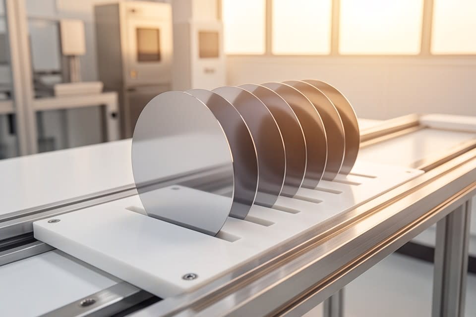
Semiconductor equipment experts commonly say that “the precision of the packaging process directly determines product reliability.” This means that even if the thickness deviation of a single chip is only a few micrometers, it directly affects the electrical characteristics and yield of the entire stacked structure. This is why process precision is discussed before simple production speed when talking about semiconductor automation equipment.
Why thickness uniformity has become a key process variable
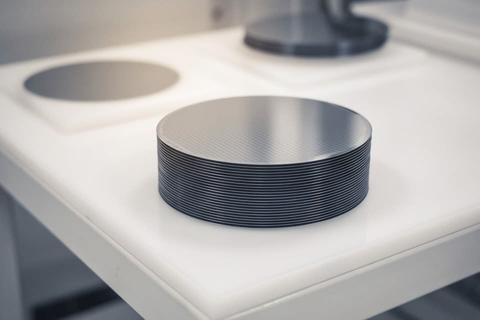
Semiconductor packaging technology is rapidly shifting from single chip structures to 3D stacked structures in which dozens of chips are stacked vertically. AI semiconductors and high performance memory products are driving this trend, and the thickness precision required inside packages is becoming increasingly stringent.
In 3D stacked structures, wafer thickness sometimes needs to be reduced from about 780μm to 10μm or less, and at this point, thickness uniformity becomes a key variable that determines whether design performance can be realized in practice. According to research published in ScienceDirect, the total thickness variation for a 300mm wafer must be achieved at 0.5μm or less to stably maintain the electrical characteristics of high performance memory devices.
As the bonding area between chips becomes narrower and the number of stacked layers increases, a single thickness deviation can compromise the reliability of the entire package. The goal is not simply to make wafers thinner, but to make them uniformly thin. Building a process environment that meets this standard has become the starting point for introducing semiconductor automation equipment.
Precision in the grinding process and automation design
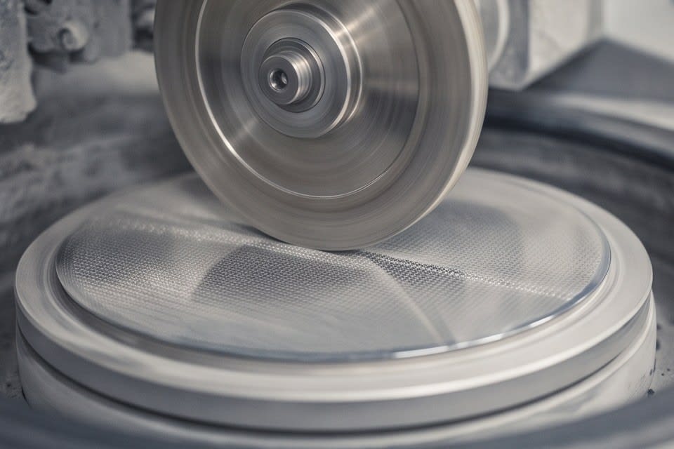
In the grinding process, the diamond wheel removes the wafer surface at the micron level to control thickness. Surface roughness and material removal rate vary significantly depending on machining conditions. According to research results, in diamond wheel grinding, surface roughness is measured in the Ra 0.486~1.118μm range, and the material removal rate is measured at 555~1546μm/h. These figures show that the range varies widely depending on condition settings, which makes precise management of process parameters essential.
Increasing grinding speed improves productivity, but it can create unwanted stress and dislocations inside the wafer, negatively affecting device performance and yield. How to balance fast removal with precise removal is the key criterion in equipment selection.
This is where grinder systems configured as Full Auto and Manual Type attract attention. The Huvics PKG Grinder combines a high precision stage with a diamond wheel and is designed to secure stable quality even in high speed processes for various package types such as FCBGA, WLCSP, and QFN/DFN. The ability to choose between Full Auto and Manual depending on the production line configuration is also a factor that enables flexible response in sites where high mix low volume production and mass production coexist. Securing precision and productivity at the same time is the core of the automated grinding process.
The role of cleaning and drying processes and integrated design
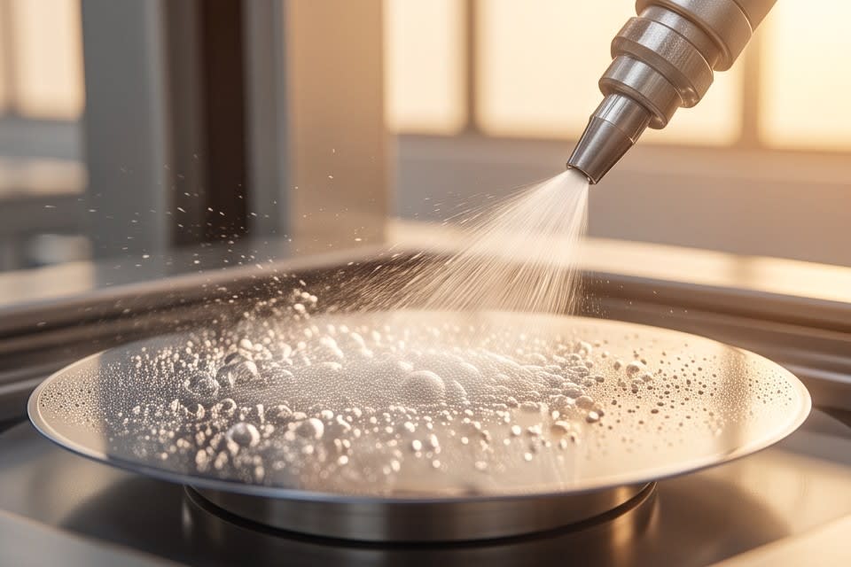
The cleaning process is often considered a post process in semiconductor manufacturing, but in reality, it is performed repeatedly enough to account for about 30% of the entire front end process. A single fine particle left on the surface after grinding or stacking can become the source of defects in the next process step. For components with high precision requirements, such as camera modules, autonomous driving sensors, and VCM motors, the completeness of the cleaning process plays an even larger role in determining final quality.
As the understanding spreads across production sites that a single cleaning method cannot effectively respond to various types of contamination, methods that combine multi step cleaning technologies such as micro bubbles, water jets, and air knives are gaining attention. The Huvics Cleaner System integrates oven drying with these multi step cleaning technologies to reduce the possibility of secondary contamination caused by residual moisture after cleaning.
As particle removal efficiency improves, the defect rate decreases, and that result leads directly to final yield. The perspective of designing the cleaning process not as an independent step but within the flow of the overall automation equipment is becoming established, and this shift is significant in that it is redefining semiconductor production efficiency.
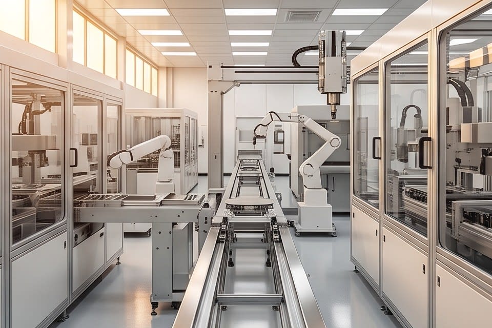
The competitiveness of semiconductor automation equipment ultimately depends on how precisely and consistently each process is connected. From the grinding process that controls thickness uniformity, to the automation system that precisely controls machining conditions, to multi step cleaning that removes fine contamination, these three process principles do not operate independently but work together as one yield management system. This is why integrated design between processes should be reviewed before the specifications of individual equipment when considering equipment introduction.
Huvics is an advanced technology company that develops and manufactures automation equipment and
production systems across the semiconductor, LED, Mobile, and Cosmetic industries.
With top talent and continuous technological innovation, we support customer productivity improvement and
quality competitiveness.
Huvics Contact Information
Phone: 031-374-8285
Email: cdpark@huvics.com
