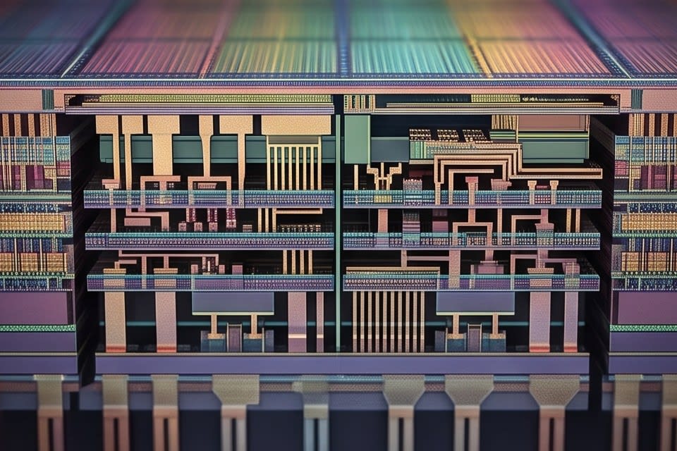
Just a few years ago, thickness variation in semiconductor package processes was regarded as something to be managed. However, as AI semiconductors have evolved into structures that vertically stack dozens of chips, micron-level thickness differences have emerged as a variable that can affect overall yield. This is why the grinder process is receiving renewed attention in advanced packaging sites, and as package integration density continues to increase, the importance of this process will grow even further.
Why Thickness Variation Determines Yield
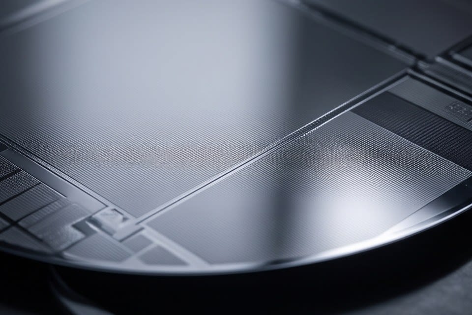
Stacking chips also means stacking errors. In stacked packages such as HBM (High Bandwidth Memory) or FCBGA (Flip Chip Ball Grid Array), the thickness of each die must fall within the specified tolerance for alignment and bonding to be performed properly. If even one layer falls outside the thickness specification, bonding integrity between upper and lower layers breaks down, and signal efficiency and bandwidth decline to a measurable degree.
According to the Siemens semiconductor packaging blog, in the sub-terahertz frequency band, even micron-level dielectric thickness variation can substantially reduce signal efficiency, bandwidth, and beamforming accuracy. Surface roughness is also an important management indicator. Patent literature specifies that surface roughness after grinding should be controlled within the range of 0.05–0.12 micrometers, and if it falls outside this range, adhesion reliability in subsequent stacking processes decreases and defects spread across the entire package.
Thickness variation is not visible to the eye, but it appears directly in yield. Since the tolerance is measured in microns while the result affects the entire yield, the key lies in how precisely the package grinding process is controlled.
Grinding Principle and Process Design of the PKG Grinder
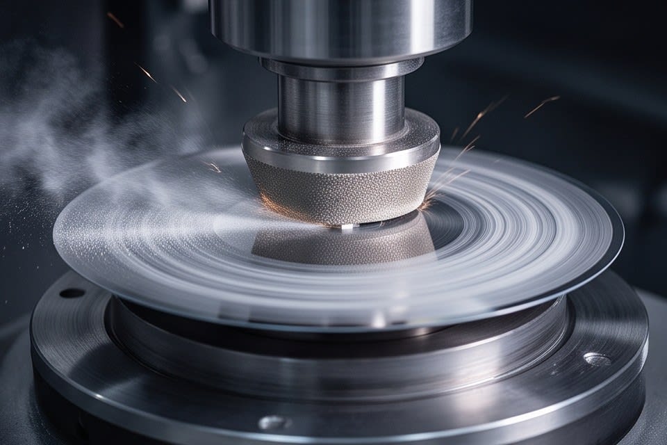
The core of process design is finding the balance point that secures both precision and productivity. Increasing grinding speed improves throughput, but it also creates the dilemma of greater wafer warpage. In the industry, it has been reported that after grinding an 8-inch wafer, warpage can reach approximately 2.20 mm, so if this is not considered in advance during process condition design, the entire downstream process can be affected.
Huvics PKG Grinder is designed to combine a high-precision stage with a diamond wheel to achieve uniform grinding at the micron level. It can stably process various package types such as FCBGA, WLCSP, QFN·DFN, and solar cells to the target thickness, and supports both Full Auto and Manual modes to ensure flexibility in production line configuration.
Minimizing quality variation even under high-speed process conditions was the key challenge in the design of this equipment, and yield changes depending on where the balance between speed and precision is set. Ultimately, the value provided by the PKG Grinder is not simply thickness reduction, but is realized by stably maintaining consistent quality without variation across the overall process.
How the Cleaning Process Completes Yield
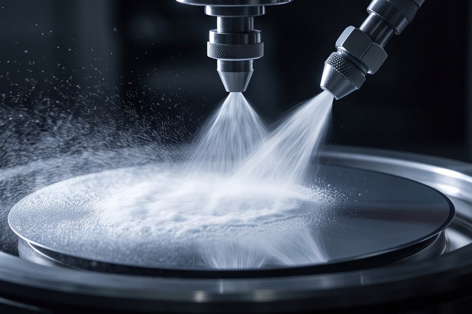
The process does not end when grinding is complete. During grinding, various contaminants such as slurry residues, metal fine particles, and organic matter remain on the surface. If these are not removed, bonding defects occur in subsequent bonding or mounting processes, and the thickness uniformity that was precisely controlled earlier becomes meaningless. Since what remains on the surface becomes a variable in the next process, cleaning is not a finishing step but an extension of yield.
In similar cases, methods using micro-nanobubbles with a diameter of 0.1 micrometers or less are being applied to remove organic matter from semiconductor surfaces, and research has also shown that an acoustic jet flow cleaning device using microbubble arrays removes particle contamination with 92.5% cleaning efficiency. Huvics Cleaner System uses a multi-step cleaning method that combines microbubbles, water jet, and air knife to remove surface contamination step by step after grinding.
As the integration density of AI semiconductor packages increases, the acceptable contamination level becomes even lower, and the precision standards required for the cleaning process are also rising.
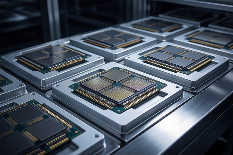
The grinder process is not simply a task of making chips thinner. Yield is completed only when a series of steps, from securing micron-level thickness uniformity to thoroughly cleaning the surface after grinding, is connected as one flow. Just a few years ago, the objective was to make it sufficiently thin, but now the standard is to make it uniform and clean. As package integration density increases, this standard will become even stricter, and the precision of process design will become the starting point of product competitiveness.
Huvics is an advanced technology company that develops and manufactures automation equipment and
production systems across the semiconductor, LED, mobile, and cosmetic industries.
With top talent and continuous technological innovation, we support customers in improving productivity and
securing quality competitiveness.
Huvics Contact
Phone: 031-374-8285
Email: cdpark@huvics.com
