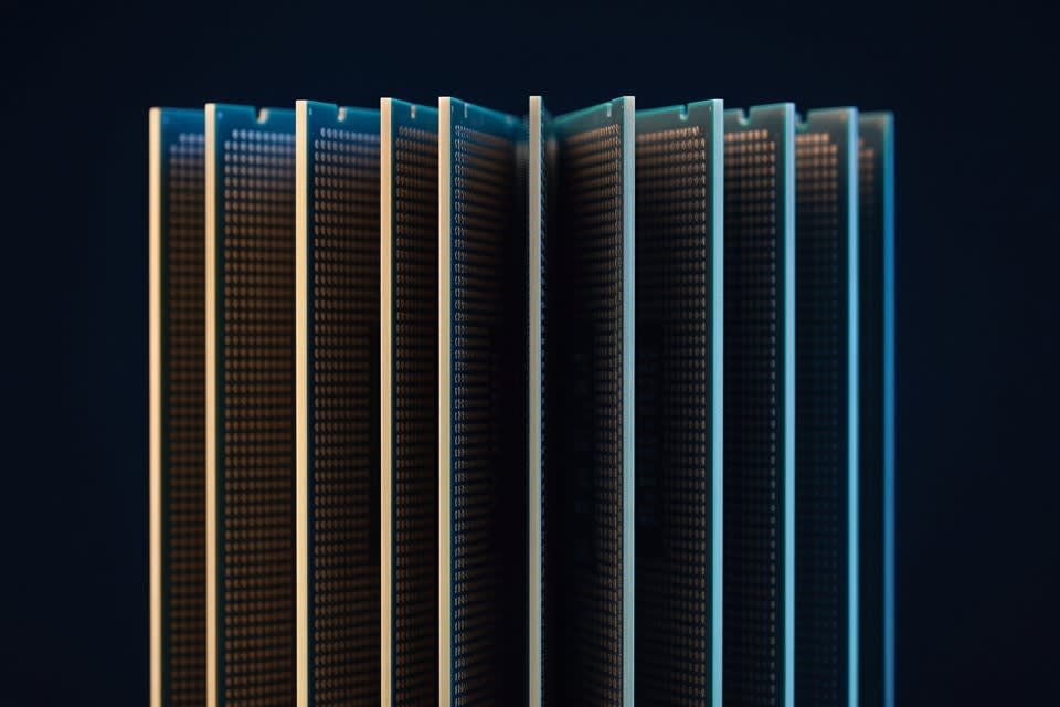
According to recent reports, demand for AI semiconductors and high-performance memory is rising rapidly, further increasing the required precision of semiconductor packaging processes. As 3D stacked packaging, which improves performance by stacking chips vertically, emerges as a key technology, micron-level thickness control is becoming a critical factor that determines yield and reliability on the manufacturing floor. This shift presents a direct challenge to everyone involved in designing or operating semiconductor packaging processes.
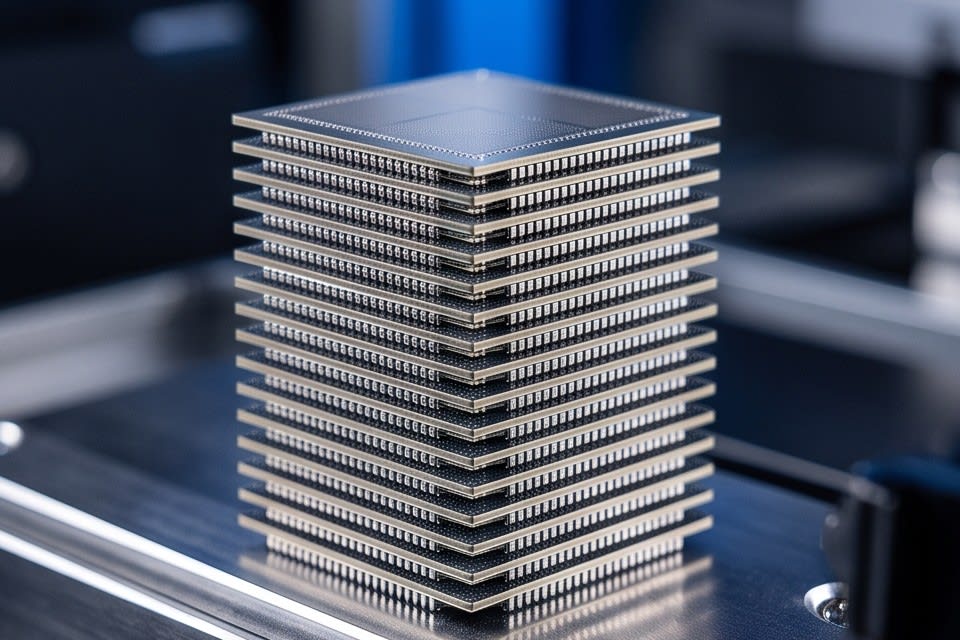
Why Thickness Uniformity Matters in Stacked Packaging
Stacking chips also means stacking tolerances. In 3D IC stacked structures, wafers must be processed from a thickness of about 780μm down to less than 10μm. If thickness is not uniform during this process, the thermo-mechanical reliability of the entire chip after stacking drops sharply. When a thinned wafer is uneven, stress is distributed unevenly across the bonding surface, which can lead to cracks or interlayer separation under long-term operating conditions.
The same applies when external particles become trapped between wafers during stacking. A single particle can create a localized thickness variation, and that variation can cause delamination and interlayer separation, reducing bonding quality and yield at the same time. For this reason, controlling the total thickness variation of the wafer, TTV, to 1μm or less has become an industry benchmark in ultra-precision grinding processes.
Looking only at the numbers, the requirement may seem simple. In actual mass production, however, consistently meeting this standard is an entirely different challenge. Even within a single wafer, thickness can vary depending on location, and equipment vibration, temperature changes, and subtle differences in grinding speed all affect TTV. In the end, the success of stacked packaging depends on how uniformly the wafer can be ground, making precision the decisive factor.
How Mechanical Grinding Achieves Thickness Uniformity
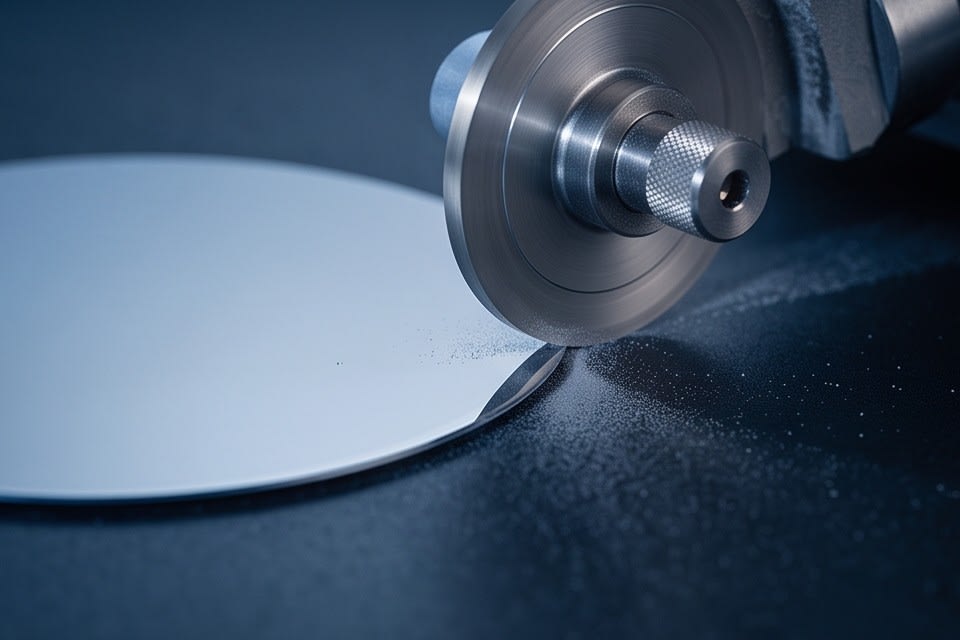
Two main methods are used to secure thickness uniformity: mechanical grinding and CMP, chemical mechanical polishing. CMP planarizes the surface by using chemical reactions and mechanical friction at the same time, while mechanical grinding directly removes material from the wafer using a diamond wheel, allowing it to reach the same target thickness in less time.
The speed advantage is clear, but fast grinding alone is not enough. The process must also include control capabilities that detect thickness variation in real time and correct it immediately during grinding. Research showing that a real-time closed-loop TTV control system can reduce TTV by up to 72.2% within a single grinding process supports this point.
Huvics PKG Grinder is based on this mechanical grinding technology and combines a high-precision stage with a diamond wheel to achieve micron-level precision processing. Since thickness targets and tolerances differ by package type, such as FCBGA, WLCSP, and QFN/DFN, it is important for equipment to be configured to respond flexibly to diverse package specifications. With both Full Auto and Manual types available, it can be selectively applied according to the automation level of the production line. The grinding process is implemented in a way that satisfies both precision and flexibility at the same time.
The Meaning of Thickness Uniformity in AI and High-Performance Memory Production
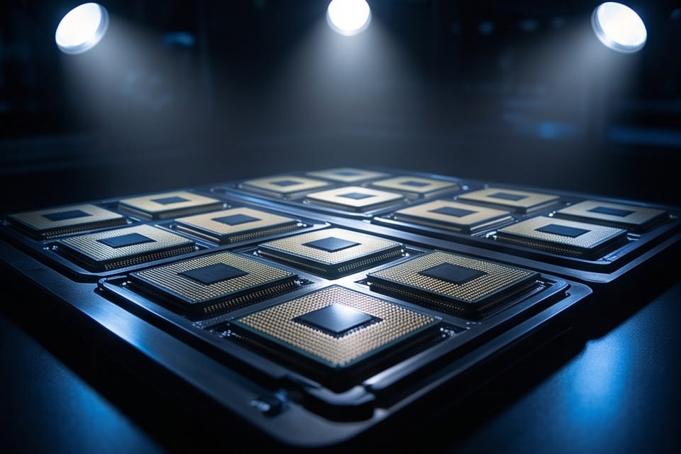
As demand for AI accelerators and high-bandwidth memory, HBM, grows rapidly, the requirements for packaging processes are also rising. In particular, AI packaging environments have shown that micron-level dielectric thickness variation can reduce system efficiency, data transmission bandwidth, and beamforming accuracy to a measurable degree. No matter how precisely circuits are designed, thickness variation in the packaging process can prevent the final product from reaching its intended performance targets.
In this context, the idea that performance is completed not in design but in process becomes especially clear. For this reason, in production sites for AI semiconductors and high-performance memory, the key selection criterion is not simply the ability to grind thinly, but equipment reliability that can maintain stable thickness uniformity even during high-speed processing. PKG Grinder is designed to maintain stable quality under high-speed process conditions and achieve high yield, responding to the needs of production environments that require both yield and process stability. As stacked packaging technology becomes a key factor determining next-generation semiconductor performance, technological competition around grinding process precision is becoming even more intense.
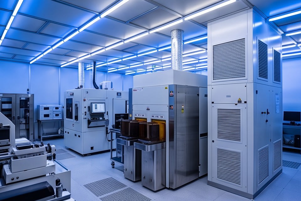
Ultimately, the quality of stacked packaging is determined not by the design drawing, but by the precision of the grinding process. In a structure where the ability to control thickness uniformity to 1μm or less determines both yield and reliability, choosing process equipment is not simply an investment in facilities, but a decision that shapes product competitiveness. The packaging precision standards required in the AI semiconductor era are continuing to rise, and consistently meeting those standards on actual mass production lines remains the key challenge ahead.
Huvics is an advanced technology company that develops and manufactures automation equipment and
production systems across the semiconductor, LED, Mobile, and Cosmetic industries.
With top talent and continuous technological innovation, we support customers in improving productivity and
securing quality competitiveness.
Huvics Contact
Phone: 031-374-8285
Email: cdpark@huvics.com
