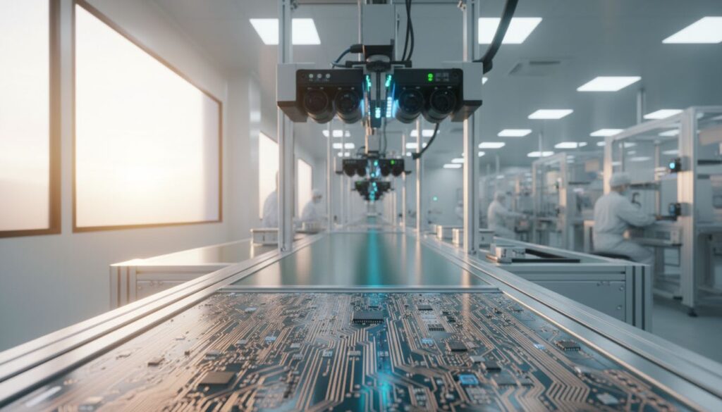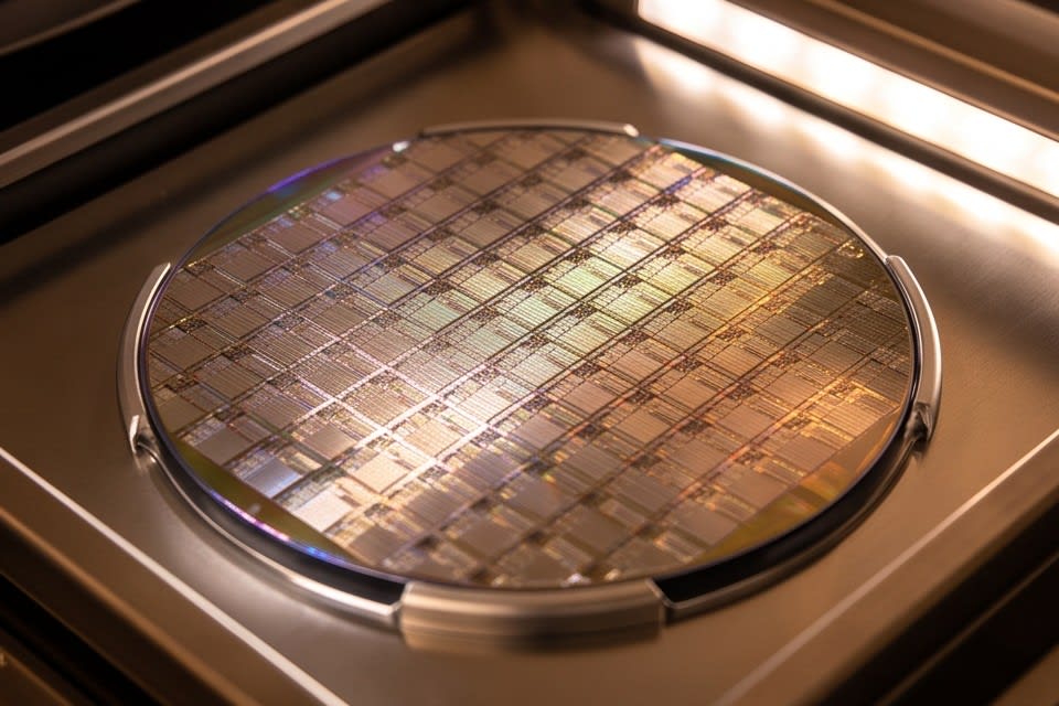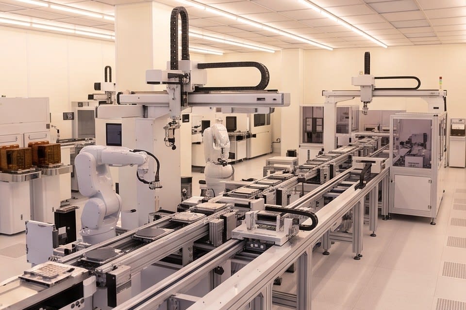
Many managers at semiconductor manufacturing sites still lack a clear view of the specific causes of cost loss at each process stage. As a result, yield gradually declines again and again, or defects are discovered only in the back-end process, causing the costs already invested to be lost entirely. If you have never examined in numbers where and how much loss occurs in each process, you are already missing the starting point for reducing unit cost.
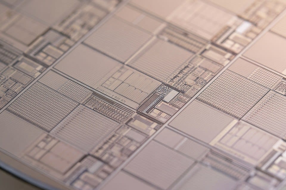
A 1% Yield Difference Can Decide Millions of Dollars
Semiconductor manufacturing unit cost ultimately comes down to yield. Hundreds of processes are interconnected before a single chip is completed, and contamination or thickness non-uniformity in any one stage can instantly consume the value of every process that follows.
According to an analysis by Applied Physics USA, in a production environment where more than 500 chips are loaded on a 300mm wafer, just a 1% drop in yield results in a loss of 1.5 million dollars per production run. The same data also states that detecting defects before the lithography process can save 5,200 dollars per wafer. What these figures show is simple. How early defects are caught determines unit cost.
According to data from the United States Patent and Trademark Office, yield loss caused by particle contamination in the metal process stage reaches 6.8%, more than twice the 2.7% loss rate in the polysilicon process. Each process stage carries a different level of contamination risk, and understanding that weight accurately is emerging as the first condition for process dieting.
Cleaning and Grinding, the Two Axes of the Unit Cost Equation
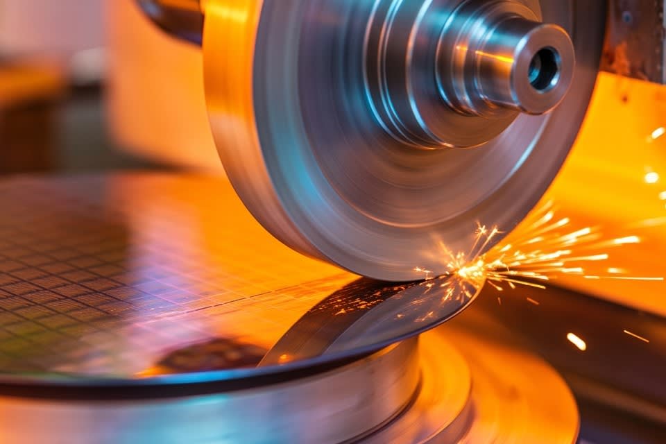
Cleaning and grinding are the two sides of the semiconductor manufacturing unit cost equation. How uniformly and thinly a wafer can be ground, and how completely contamination particles can be removed from the surface, determine both yield and cost.
In the backgrinding process, logic gates are ground to about 100µm, DRAM memory to about 50µm, and MEMS devices to about 30µm. As thickness decreases, allowable tolerance becomes narrower. According to industry standards cited by Semiconductor Digest, even at a final thickness of around 20µm, thickness tolerance must be maintained at 1µm or less. If grinding precision fluctuates even slightly, every process built on top of it fluctuates as well.
The cleaning process is no different. According to Hielscher Ultrasonics, liquid jets formed by ultrasonic cavitation disperse particle aggregates at speeds reaching 1000km per hour. If this principle is not precisely controlled, fine particles left on the surface become variables that affect the quality of the entire downstream process. This is why multistage cleaning methods that combine micro bubbles, water jets, and air knives step by step are gaining attention.
How the precision of both cleaning and grinding is secured and maintained is the practical key to process dieting.
Blocking Defects at the Beginning of the Process
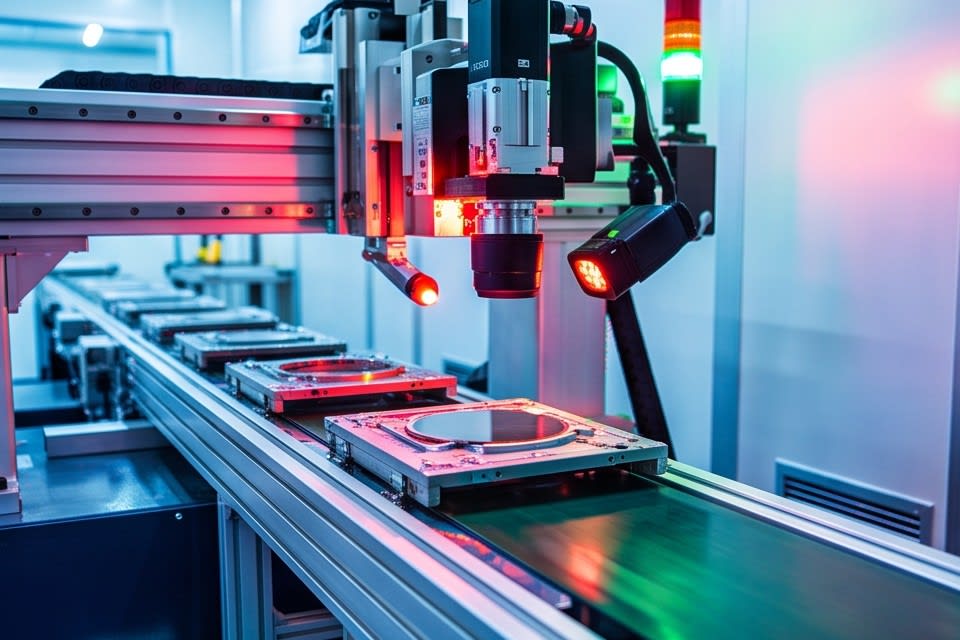
From the perspective of manufacturing site managers, the situation they most want to avoid is discovering defects only in the back-end process. A single defect missed at the front end can invalidate all costs invested in subsequent processes.
Huvics combines proprietary ultrasonic dispersion technology with vision inspection algorithms to implement a method that blocks this issue at the beginning of the process. While material particles in liquid are uniformly dispersed at the micro level, vision algorithms detect defects in fine patterns in real time and control process variability. In MLCC and FPCB processes, the convergence of these two technologies functions as a direct means of improving quality stability.
Issues repeatedly encountered in the field, such as defects in semiconductor tape bonding processes, challenges in semiconductor tray cleaning, and foreign material defects in camera modules, also find solution paths through the same technological structure. As early process assembly reliability is secured, back-end rework costs and defect handling costs decrease, and those savings directly lead to improved unit cost. This is where the meaning of managing cleaning, inspection, and grinding precision in one integrated flow can be seen in unit cost dieting.
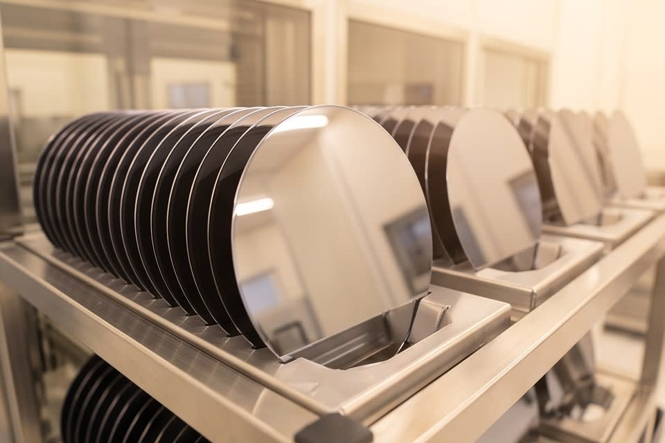
Reducing semiconductor manufacturing unit cost cannot be solved by changing only one process. Only when the points where contamination occurs, the sections where thickness deviations accumulate, and the flow where defects appear too late are examined from the perspective of the entire process does it become clear where costs are leaking. In an environment where a single-digit difference in yield can decide millions of dollars, managing the precision of cleaning and grinding from the beginning of the process is the quietest and most reliable path to reducing unit cost.
Huvics is an advanced technology company that develops and manufactures automation equipment and
production systems across the semiconductor, LED, Mobile, and Cosmetic industries.
With top-tier talent and continuous technological innovation, we support customers in improving productivity and
securing quality competitiveness.
Huvics Contact
Phone: 031-374-8285
Email: cdpark@huvics.com