Tag: Huvics

  • Why Semiconductor Packaging Reliability Must Be Managed Step by Step from Grinding to Cleaning

    Why Semiconductor Packaging Reliability Must Be Managed Step by Step from Grinding to Cleaning

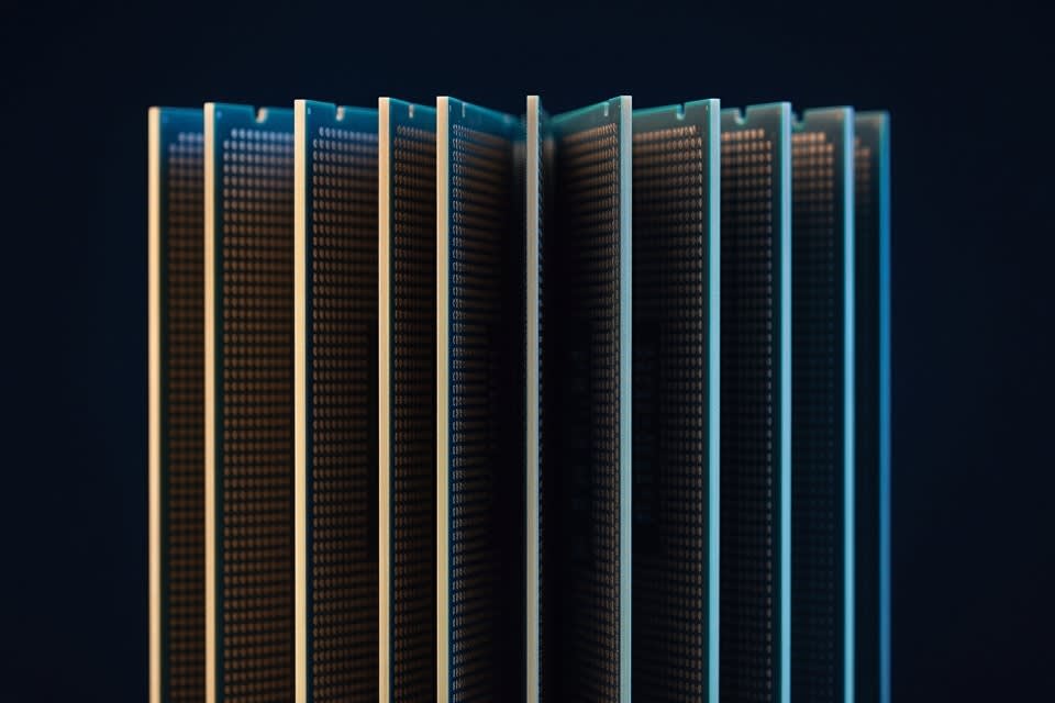
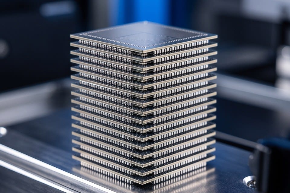
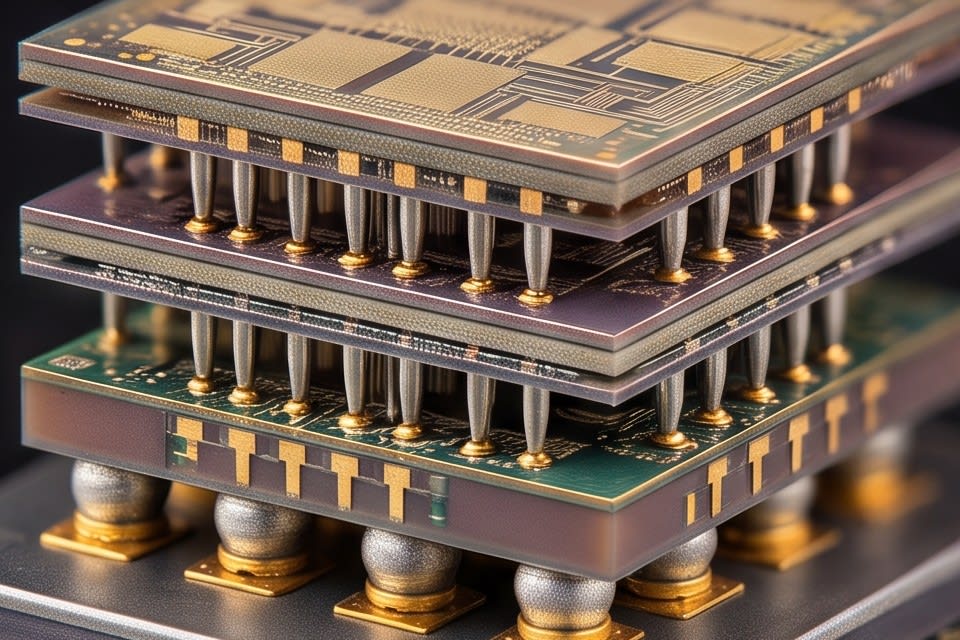
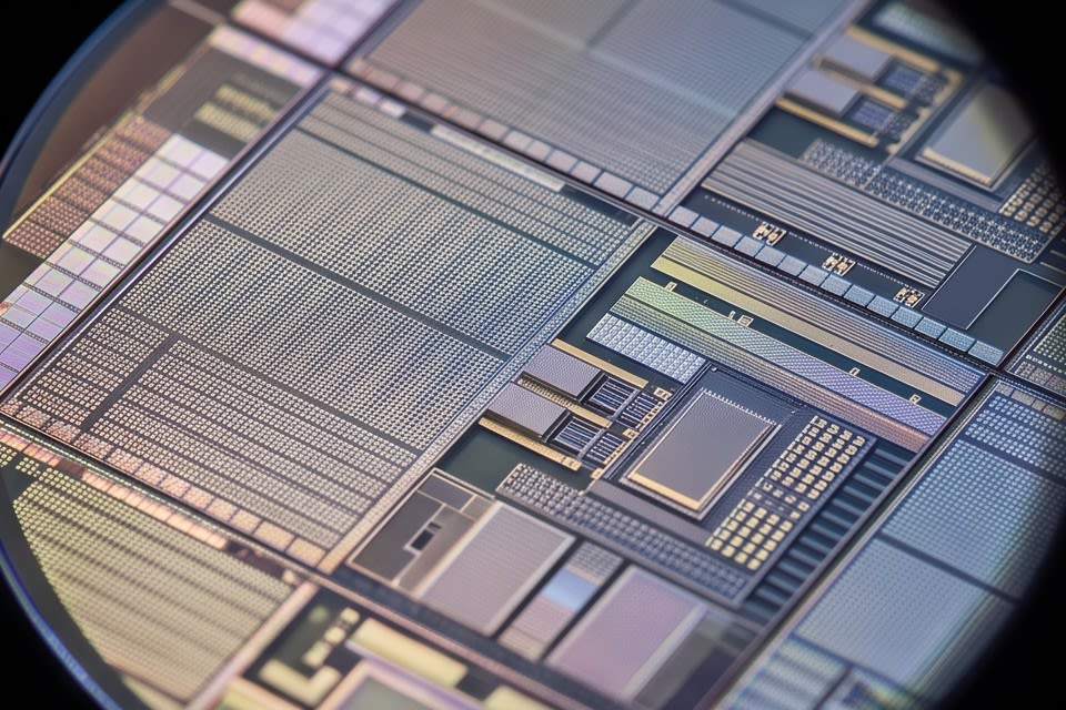
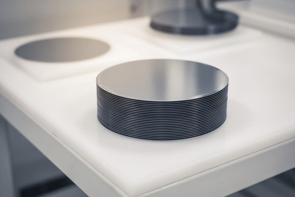
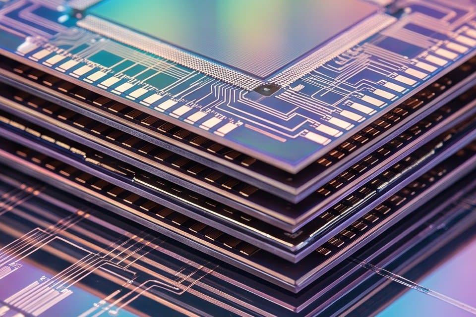
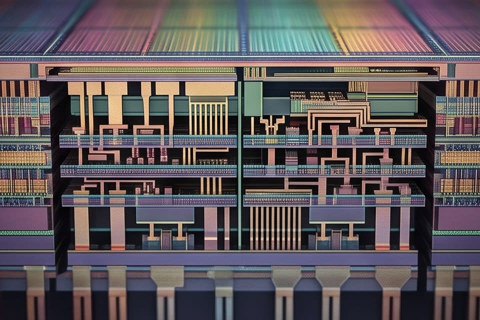
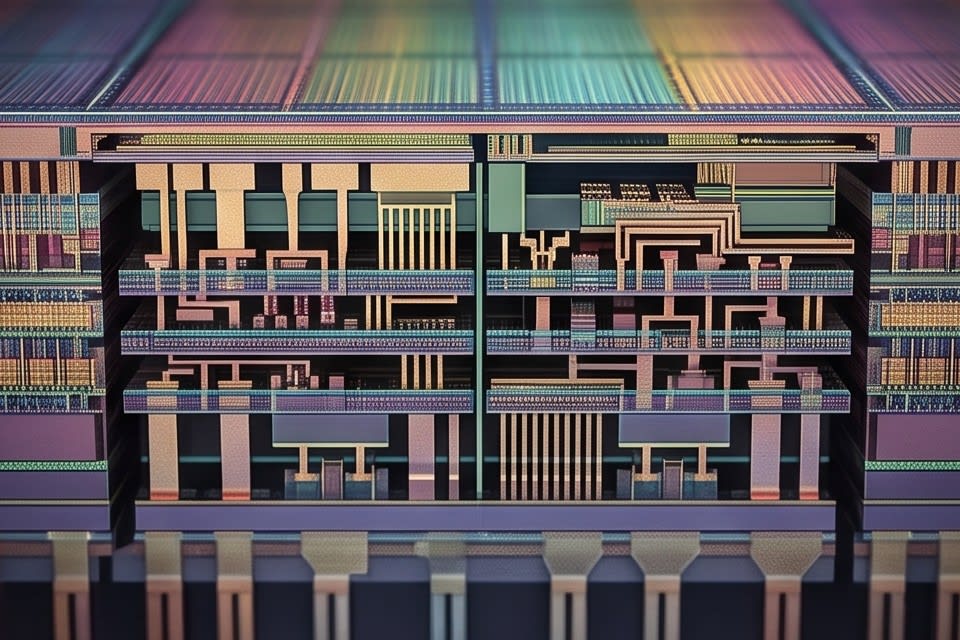
    Cross sectional structure of high performance semiconductor chips stacked vertically in multiple layers

    It is time to move beyond the idea that shaving a few more micrometers off the thickness of a semiconductor package will not change its performance. As demand for AI semiconductors and high performance memory grows explosively, stacked packaging that vertically stacks dozens of chips has become common, and a single thickness variation has become a factor that can shake the reliability of the entire process. This may sound exaggerated, but when you examine the defect data accumulated in actual manufacturing sites, it is far from an empty claim. Let us take a closer look at how equipment operation becomes the starting point of quality.
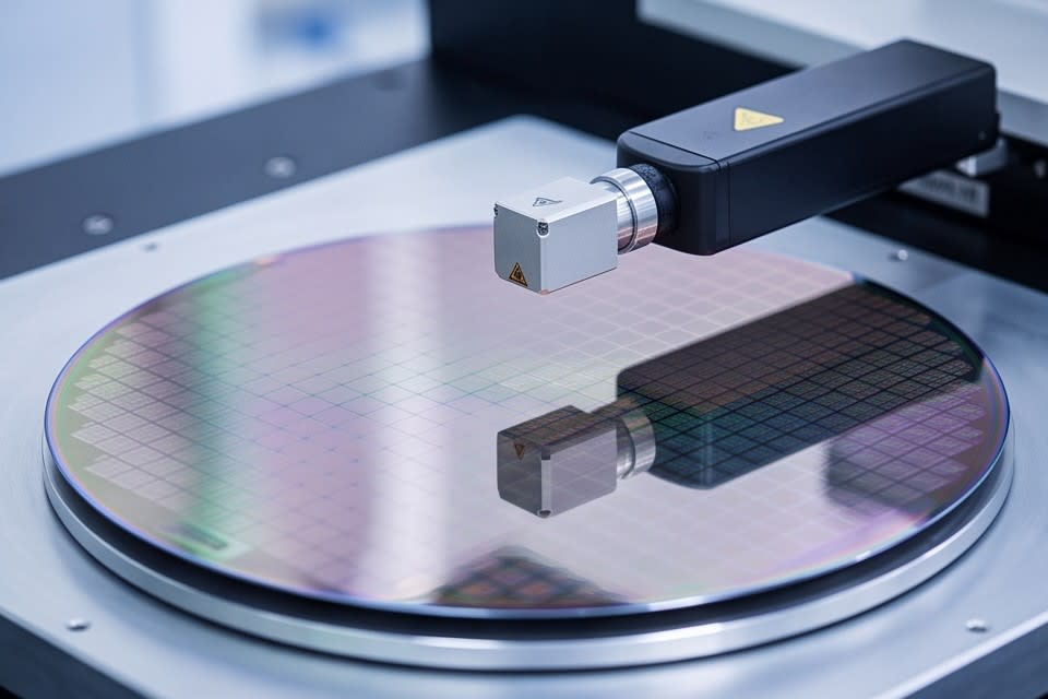
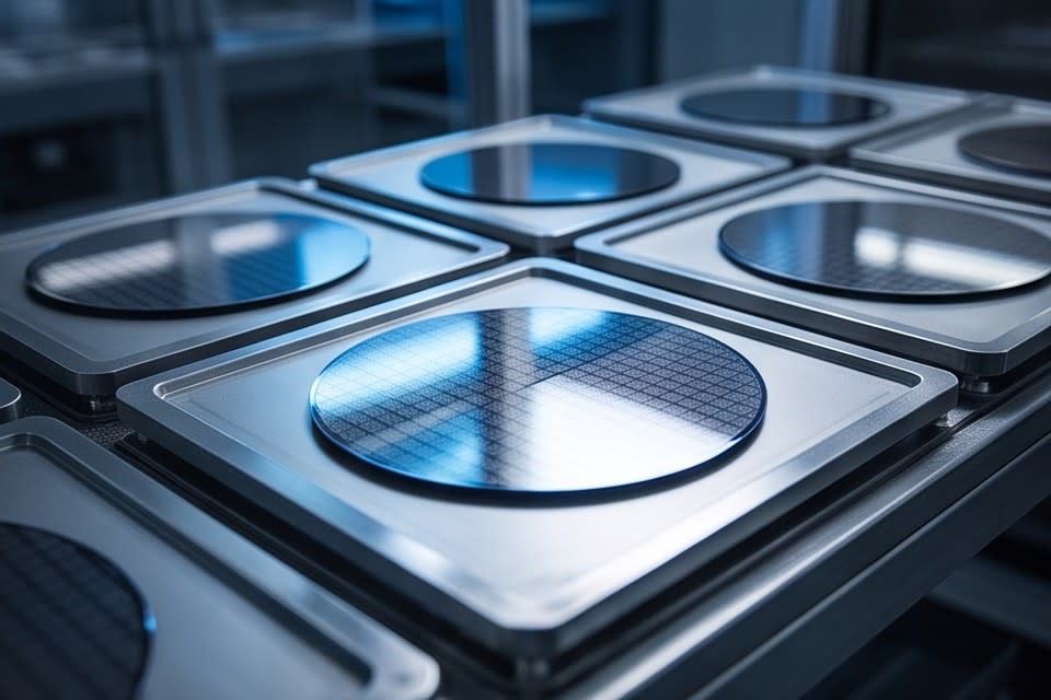
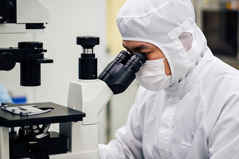
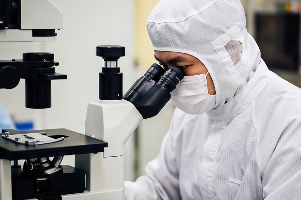
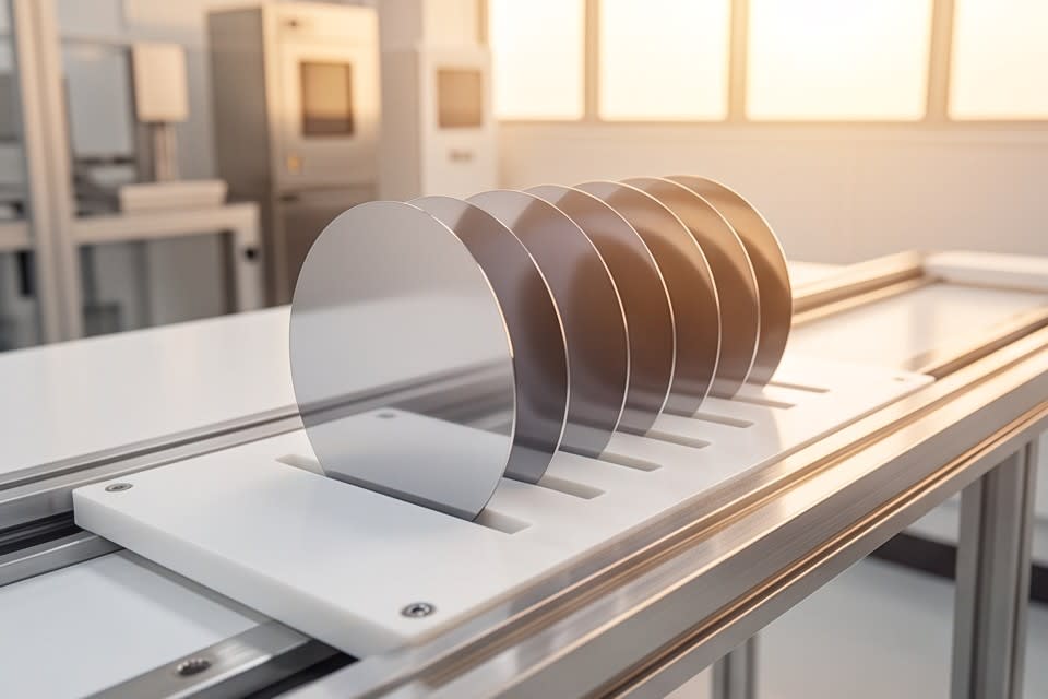
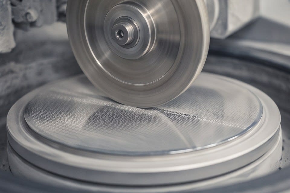
    Measurement equipment precisely inspecting semiconductor wafer thickness variation and uniformity

    Why Thickness Uniformity Determines Packaging Reliability

    In high performance semiconductor packaging, thickness uniformity is not optional. In a structure where chips are stacked in multiple layers, even a slight deviation in the thickness of each layer can create voids at the joints or concentrate stress at specific points during subsequent bonding or stacking processes. This phenomenon is not easily noticeable at first, but over time it seriously reduces electrical reliability.

    The concept of total thickness variation, or TTV, reveals this issue numerically. This is why international standards define the allowable TTV range for advanced applications at ±2 to 5 micrometers. As package types become more diverse, such as FCBGA, WLCSP, and QFN, the required machining precision becomes even higher. On manufacturing sites, allowable deviations vary by package type, and process conditions are adjusted in detail. Ultimately, the stability of the packaging process depends on how uniformly thickness can be maintained.
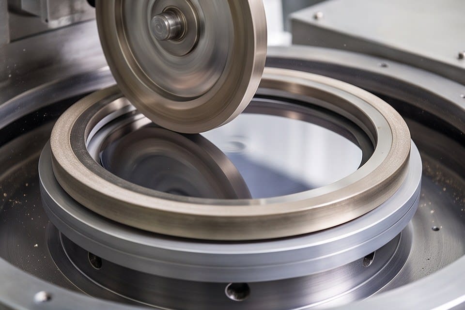
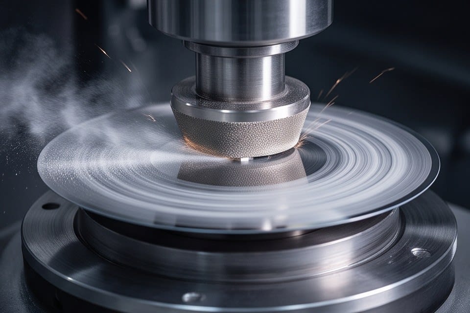
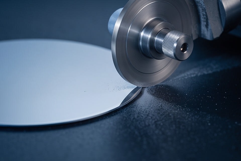
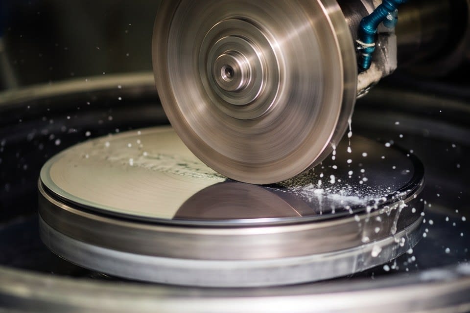
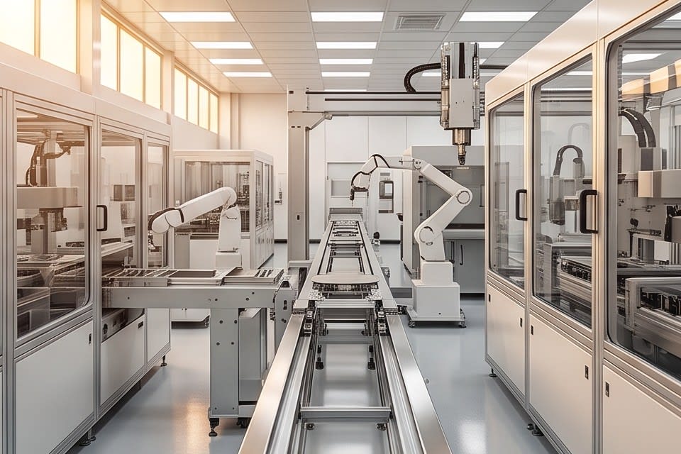
    Grinding equipment processing wafer thickness in micrometer level control

    How Grinding Equipment Operation Determines TTV Stability

    The way grinding equipment achieves TTV stability lies in the combination of mechanical precision and process design. Spindle speed, the material and grit size of the grinding wheel, and the leveling precision of the stage must work together to enable uniform machining at the micrometer level. In the industry, grinding equipment spindles are known to operate in the range of 5,000 to 60,000 RPM depending on the application and material, and selecting the appropriate speed within this range directly affects yield.

    Huvics PKG Grinder combines a high precision stage with a diamond wheel to deliver stable grinding within this range. With Full Auto A Type, B Type, and Manual Type options, line configurations can be selected flexibly, allowing the process to be designed differently according to production scale or product characteristics. The level of automation selected affects the production efficiency of the entire line, and reducing operator intervention also reduces sources of variation. Controlling TTV within specification at the grinding stage is how the foundation is prepared for all subsequent processes.
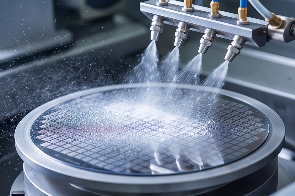
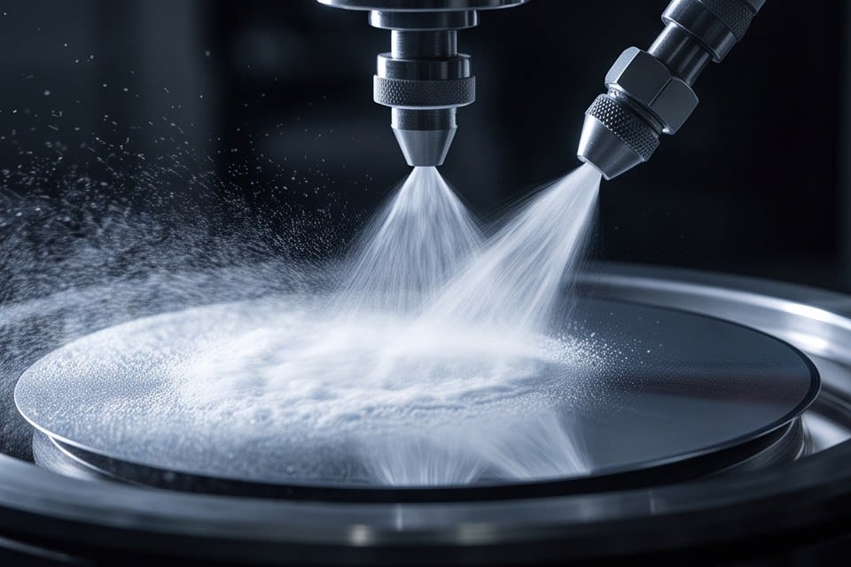
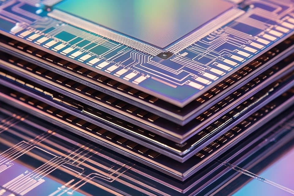
    Cleaning process spraying liquid onto the wafer surface to remove fine residues

    Why the Cleaning Process Is the Final Gateway to Packaging Quality

    Even after grinding is completed, the risk factors in the packaging process do not disappear. If fine particles and machining residues generated during grinding remain on the surface, they can lead to bonding defects or contamination in later processes. Particle Removal Efficiency, or PRE, is an indicator of how effectively a cleaning system removes surface contaminants. As device structures become finer, even very small particles can affect performance, making it increasingly important to achieve high PRE.

    In the post grinding cleaning process, it has been confirmed that controlling the pressure of the buffing disk and the flow rate of chemical solutions is effective in improving PRE. Huvics Cleaner System adopts a multi step cleaning method that sequentially applies micro bubbles, water jet, and air knife, and adjusts cleaning conditions according to products with various forms and materials, including camera modules, sensors, VCM motors, and trays. It also includes an Oven Dry function, enabling the process from cleaning to drying to be handled in one continuous flow. Managing the connected process from grinding to cleaning and drying in an integrated way, rather than separating each step, is becoming a key trend for improving packaging quality stability.
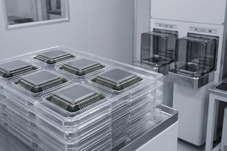
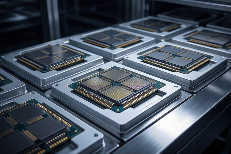
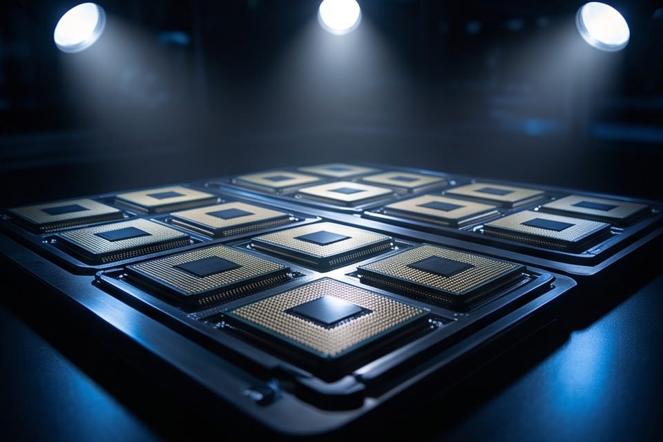
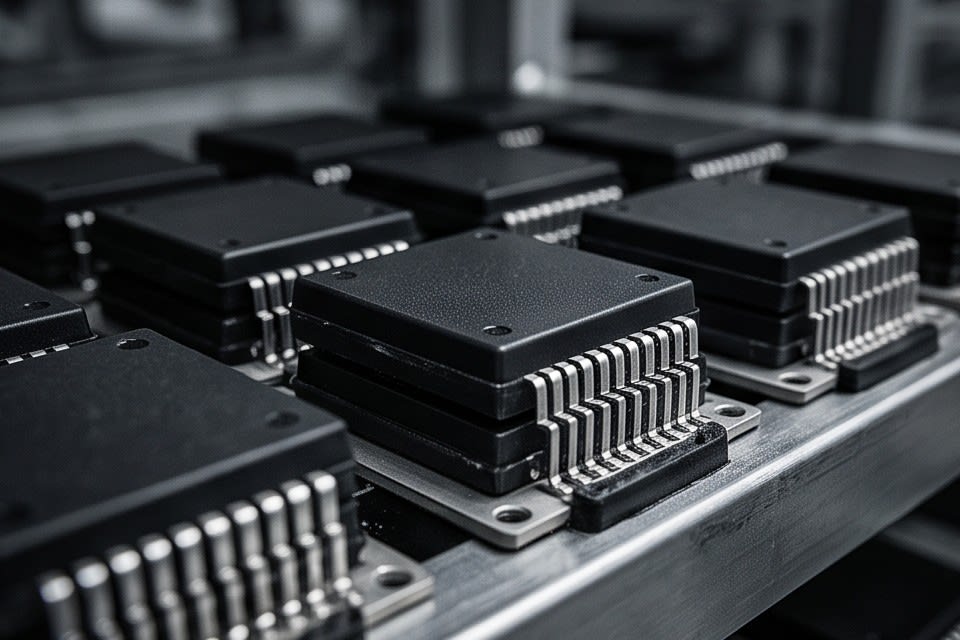
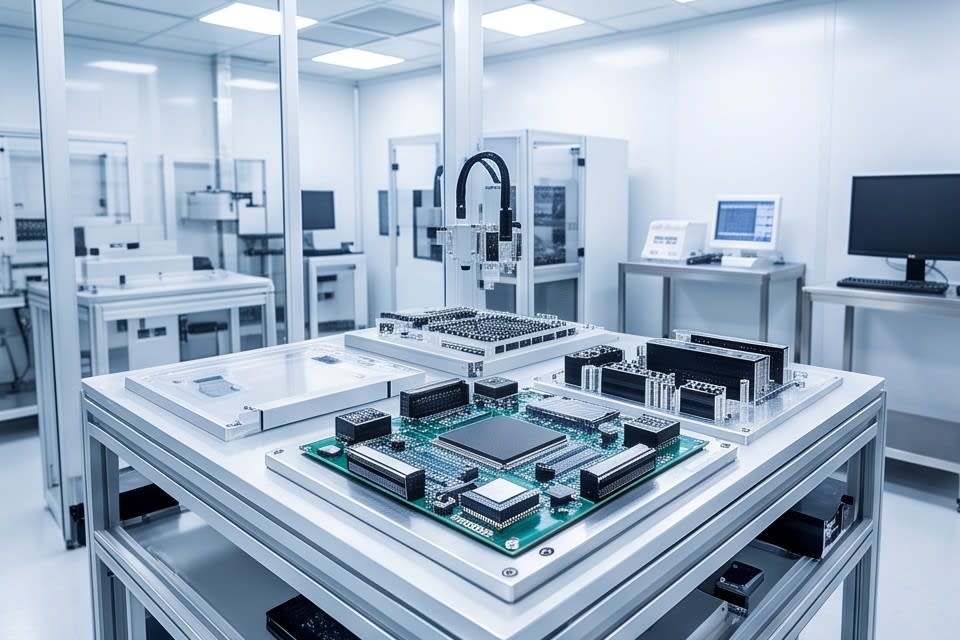
    Semiconductor packages processed with uniform thickness and clean surfaces and aligned on a tray

    Only when grinding precision and cleaning efficiency work together can the reliability of the packaging process truly be secured. Controlling thickness variation at the micrometer level and completely removing contamination particles generated during that process are quality standards for high performance packaging. The fact that the way equipment is operated directly determines the reliability level of the product prompts us to reconsider the standards by which processes should be designed and managed.


    Huvics is an advanced technology company that develops and manufactures automation equipment and
    production systems across the Semiconductor, LED, Mobile, and Cosmetic industries.
    With outstanding talent and continuous technological innovation, we support customers in improving productivity and
    securing quality competitiveness.

    Huvics Contact Information

    Phone: 031-374-8285
    Email: cdpark@huvics.com

    Contact Huvics

  • Package Grinder Process: Why Thickness Uniformity and Cleaning Determine Yield

    Package Grinder Process: Why Thickness Uniformity and Cleaning Determine Yield

    A complex and precise internal cross section of a semiconductor showing high-density stacking technology, a core element of AI semiconductors

    Just a few years ago, thickness variation in semiconductor package processes was regarded as something to be managed. However, as AI semiconductors have evolved into structures that vertically stack dozens of chips, micron-level thickness differences have emerged as a variable that can affect overall yield. This is why the grinder process is receiving renewed attention in advanced packaging sites, and as package integration density continues to increase, the importance of this process will grow even further.

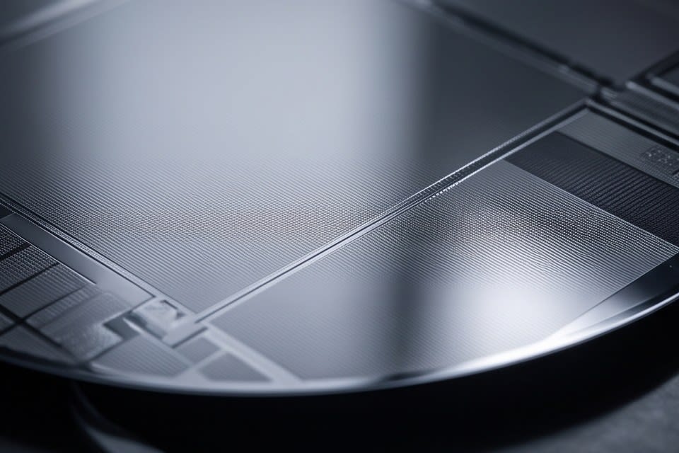
    A smooth and refined semiconductor wafer surface that intuitively visualizes thickness uniformity and surface roughness

    Why Thickness Variation Determines Yield

    Stacking chips also means stacking errors. In stacked packages such as HBM (High Bandwidth Memory) or FCBGA (Flip Chip Ball Grid Array), the thickness of each die must fall within the specified tolerance for alignment and bonding to be performed properly. If even one layer falls outside the thickness specification, bonding integrity between upper and lower layers breaks down, and signal efficiency and bandwidth decline to a measurable degree.

    According to the Siemens semiconductor packaging blog, in the sub-terahertz frequency band, even micron-level dielectric thickness variation can substantially reduce signal efficiency, bandwidth, and beamforming accuracy. Surface roughness is also an important management indicator. Patent literature specifies that surface roughness after grinding should be controlled within the range of 0.05–0.12 micrometers, and if it falls outside this range, adhesion reliability in subsequent stacking processes decreases and defects spread across the entire package.

    Thickness variation is not visible to the eye, but it appears directly in yield. Since the tolerance is measured in microns while the result affects the entire yield, the key lies in how precisely the package grinding process is controlled.

    A diamond wheel grinding the wafer surface while generating fine particles and heat

    Grinding Principle and Process Design of the PKG Grinder

    The core of process design is finding the balance point that secures both precision and productivity. Increasing grinding speed improves throughput, but it also creates the dilemma of greater wafer warpage. In the industry, it has been reported that after grinding an 8-inch wafer, warpage can reach approximately 2.20 mm, so if this is not considered in advance during process condition design, the entire downstream process can be affected.

    Huvics PKG Grinder is designed to combine a high-precision stage with a diamond wheel to achieve uniform grinding at the micron level. It can stably process various package types such as FCBGA, WLCSP, QFN·DFN, and solar cells to the target thickness, and supports both Full Auto and Manual modes to ensure flexibility in production line configuration.

    Minimizing quality variation even under high-speed process conditions was the key challenge in the design of this equipment, and yield changes depending on where the balance between speed and precision is set. Ultimately, the value provided by the PKG Grinder is not simply thickness reduction, but is realized by stably maintaining consistent quality without variation across the overall process.

    A precision spray nozzle supplying fluid to a semiconductor wafer surface and performing cleaning work

    How the Cleaning Process Completes Yield

    The process does not end when grinding is complete. During grinding, various contaminants such as slurry residues, metal fine particles, and organic matter remain on the surface. If these are not removed, bonding defects occur in subsequent bonding or mounting processes, and the thickness uniformity that was precisely controlled earlier becomes meaningless. Since what remains on the surface becomes a variable in the next process, cleaning is not a finishing step but an extension of yield.

    In similar cases, methods using micro-nanobubbles with a diameter of 0.1 micrometers or less are being applied to remove organic matter from semiconductor surfaces, and research has also shown that an acoustic jet flow cleaning device using microbubble arrays removes particle contamination with 92.5% cleaning efficiency. Huvics Cleaner System uses a multi-step cleaning method that combines microbubbles, water jet, and air knife to remove surface contamination step by step after grinding.

    As the integration density of AI semiconductor packages increases, the acceptable contamination level becomes even lower, and the precision standards required for the cleaning process are also rising.

    An array of precise packaging chips that secure uniform micron-level thickness and surface integrity

    The grinder process is not simply a task of making chips thinner. Yield is completed only when a series of steps, from securing micron-level thickness uniformity to thoroughly cleaning the surface after grinding, is connected as one flow. Just a few years ago, the objective was to make it sufficiently thin, but now the standard is to make it uniform and clean. As package integration density increases, this standard will become even stricter, and the precision of process design will become the starting point of product competitiveness.


    Huvics is an advanced technology company that develops and manufactures automation equipment and
    production systems across the semiconductor, LED, mobile, and cosmetic industries.
    With top talent and continuous technological innovation, we support customers in improving productivity and
    securing quality competitiveness.

    Huvics Contact

    Phone: 031-374-8285
    Email: cdpark@huvics.com

    Huvics Inquiry

  • Three Multistage Integrated Equipment Configurations That Solve Challenges in Semiconductor Cleaning Processes

    Three Multistage Integrated Equipment Configurations That Solve Challenges in Semiconductor Cleaning Processes

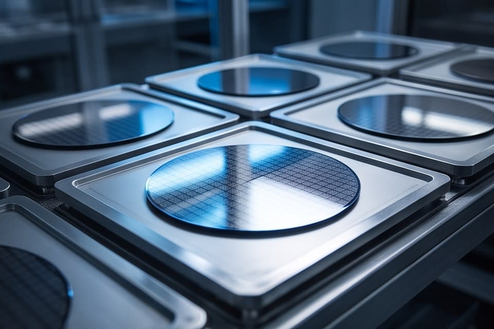
    Semiconductor wafers arranged on a tray.

    The semiconductor cleaning process is a critical stage that determines the initial quality of products on the production line. It is not simply a matter of wiping a surface, but a technical process that precisely removes invisible fine particles and contaminants according to process conditions. When cleaning lens sheets before camera module assembly, or when removing foreign matter to reuse semiconductor trays, this process is often the first barrier field engineers encounter. The cleaning method can change yield and even shift the flow of the entire line.

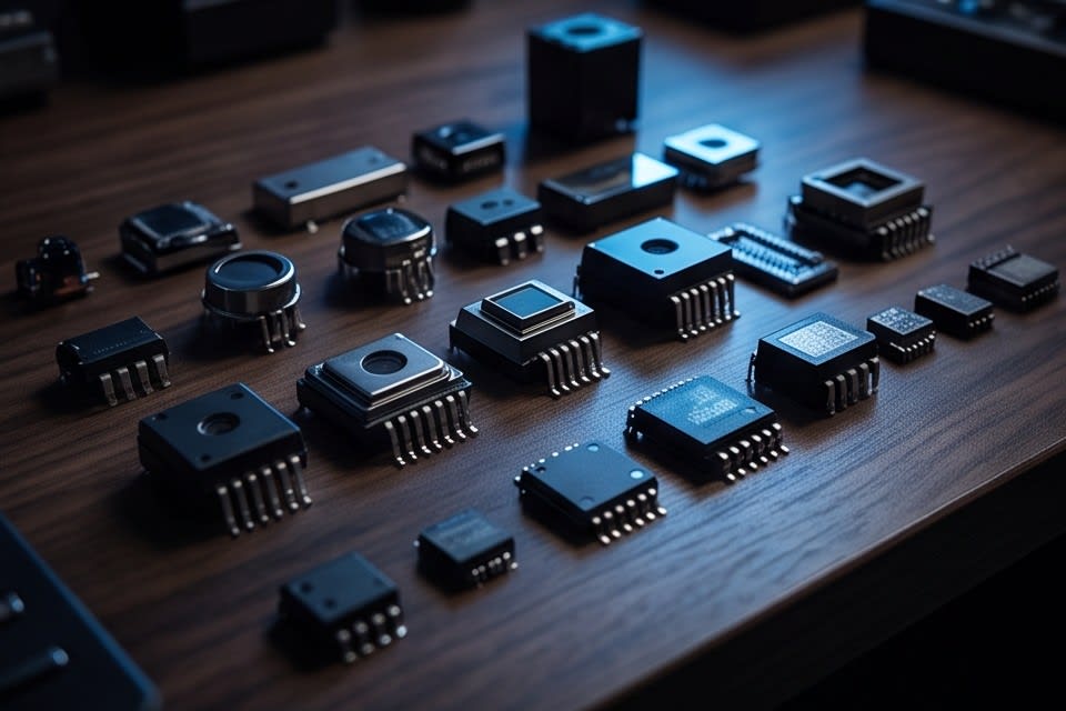
    Semiconductor packages of various sizes arranged in rows.

    Process challenges caused by diverse contamination types

    The first factor that makes the semiconductor cleaning process difficult is the diversity of contamination particles. When the cleaning target changes, such as trays, camera modules, sensors, and VCM motors, surface characteristics also change, and the size and wettability of the contaminants that must be removed vary widely. A single cleaning method cannot easily handle this diversity.

    Some particles cannot be removed by physical impact alone, while some contaminants will not detach from the surface without chemical dissolution. As semiconductor processes become more miniaturized, allowable tolerances become narrower, while contamination types become even more complex. This is why cleaning in high precision processes cannot be solved by a single standalone technology.

    Because failure in the cleaning stage affects the entire subsequent process, deciding which mechanisms to combine and in what order becomes a key criterion in process design. In the field, the approach of first identifying contamination characteristics and then selecting the cleaning technology suited to them is increasingly becoming the standard.

    A multistage cleaning system device with multiple connected tanks.

    How multistage cleaning combinations solve these challenges

    Multistage cleaning systems are gaining attention because they overcome the limits of a single technology through process combinations. Microbubbles use both chemical and physical effects, combining the oxidation reaction of the cleaning solution with the collapse impact of fine bubbles to remove surface contamination. When Water Jet is added to physically push away particles, followed by Air Knife to remove residual moisture, each stage is structured to compensate for the weaknesses of the others.

    According to a study published in the Korean Journal of Chemical Engineering, an acoustic bubble array based cleaning device achieved up to 92.5% cleaning efficiency on semiconductor wafers. The drying stage after cleaning also needs to be designed as an integrated flow rather than a separate process to prevent secondary contamination caused by residual moisture. The Cleaner System from Huvics, which combines oven drying with this multistage configuration, is designed to handle everything from cleaning to drying within a single line.

    When particle removal efficiency improves, the defect rate decreases, and when the defect rate decreases, the stability of the entire process is secured. Ultimately, which technologies are combined and how many stages are used become the key factors that determine the quality level of the cleaning process.

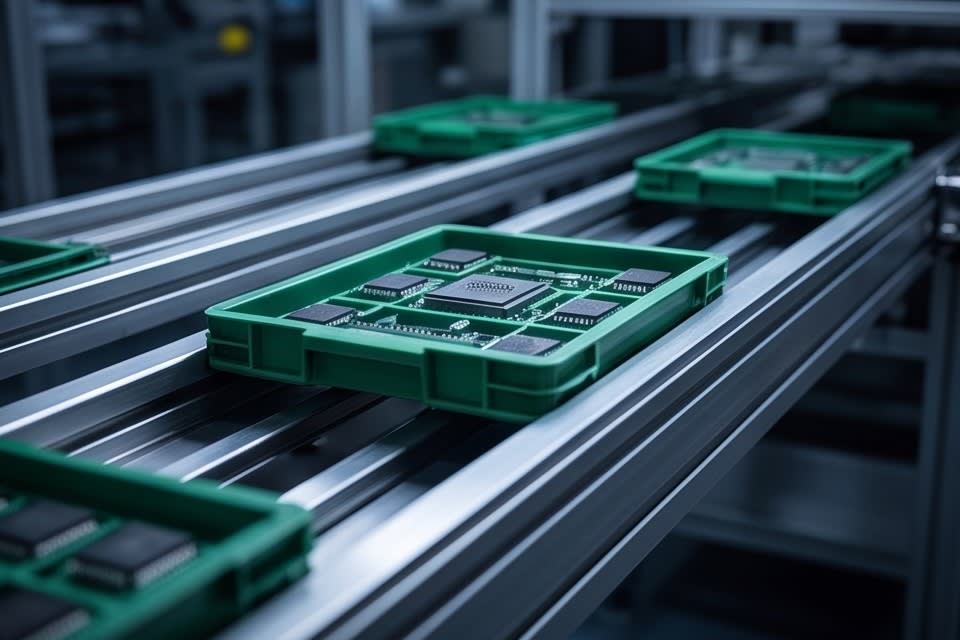
    A tray loaded with semiconductor packages moves along a conveyor belt.

    Why integrated equipment is needed for tray cleaning and grinding precision

    Field challenges in semiconductor tray cleaning

    Semiconductor tray cleaning is one of the challenges that repeatedly appears in the field. Fine foreign matter remaining on the tray surface can cause contact defects or contamination during the chip loading process, which may lead to reduced yield across the entire line. Automated tray cleaning systems are known to process approximately 30,000 units per day, and to maintain this throughput reliably, equipment design must secure both cleaning quality and speed at the same time.

    The meaning of grinding precision in package processes

    Along with cleaning issues, grinding precision also serves as a key variable in semiconductor package processes. Each package type, such as FCBGA, WLCSP, and QFN·DFN, requires different thickness specifications, and tolerances for uniformity and flatness are becoming increasingly narrow. The PKG Grinder from Huvics uses a high precision stage and diamond wheel to achieve micron level thickness processing, and it can be configured selectively as Full Auto or Manual Type, allowing flexible application according to production line conditions.

    Cleaning and grinding may appear to be separate issues, but the value of integrated equipment becomes clear when approached from the perspective that both processes are early stages that determine the final reliability of the package.

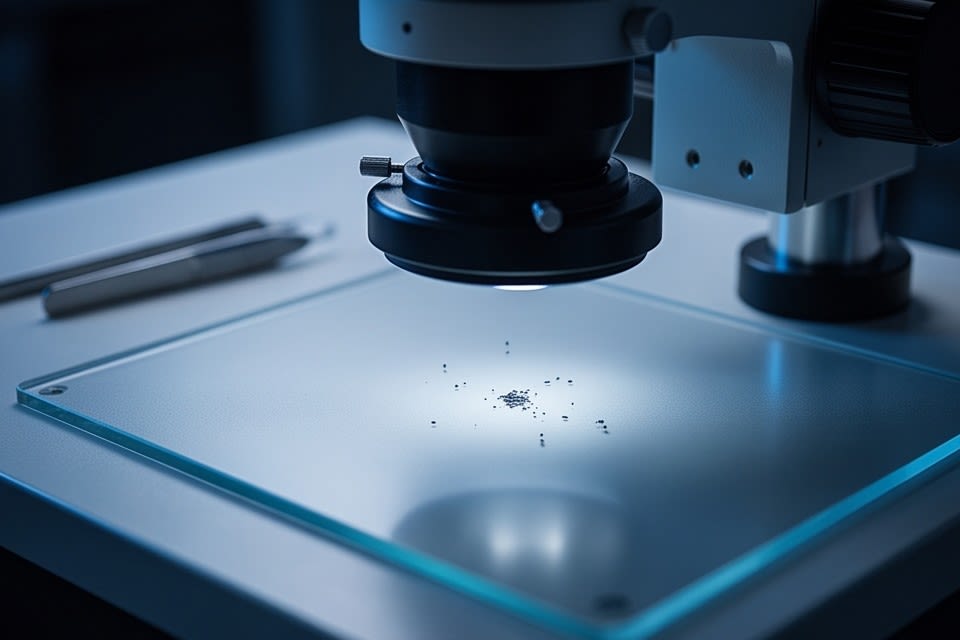
    Analyzing contamination sources by observing fine particles through a microscope.

    The challenges of the semiconductor cleaning process begin with the diversity of contamination types and the fact that process conditions differ by product. Multistage combinations rather than a single technology, integrated design of cleaning and drying, and integrated equipment configurations that also include grinding precision are becoming practical solutions in the field. No matter what process challenge you face, the starting point of equipment design is to accurately understand the nature of the contamination.


    Huvics is an advanced technology company that develops and manufactures automation equipment and
    production systems across the semiconductor, LED, Mobile, and Cosmetic industries.
    With top tier talent and continuous technological innovation, we support customers in improving productivity and
    securing quality competitiveness.

    Huvics Contact

    Phone: 031-374-8285
    Email: cdpark@huvics.com

    Huvics Inquiry

  • AI Semiconductor Stacked Packages: Why the Grinding Process Became the Starting Point for Yield

    AI Semiconductor Stacked Packages: Why the Grinding Process Became the Starting Point for Yield

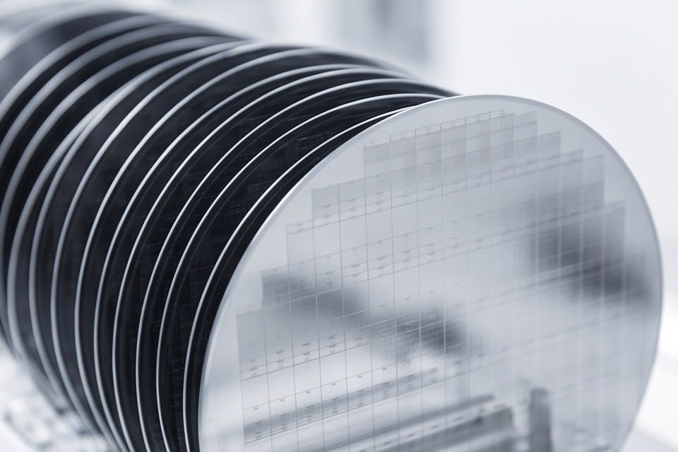
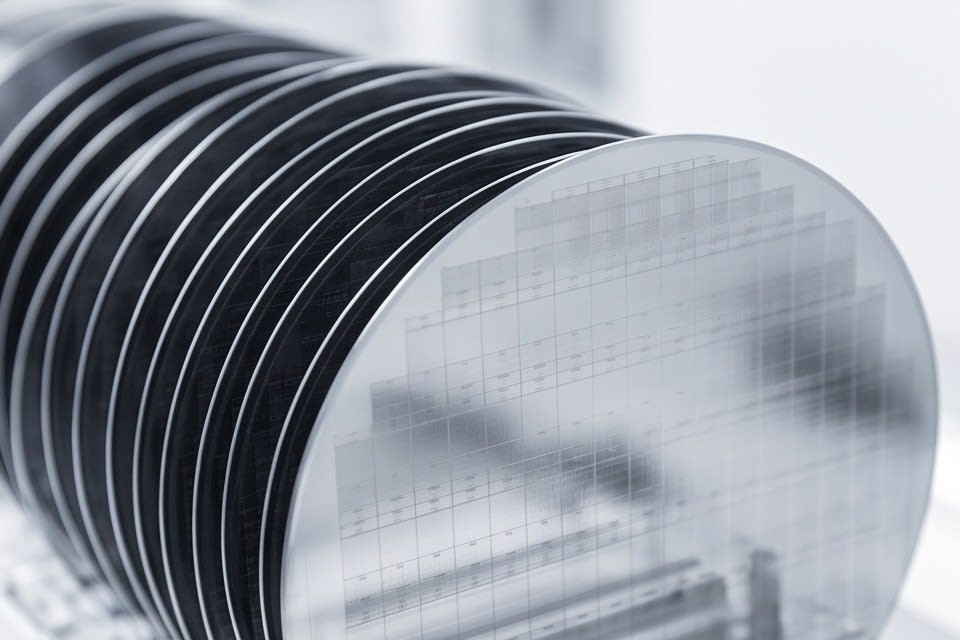
    Multiple wafers stacked vertically

    In semiconductor packaging, controlling thickness was long regarded as simply grinding materials thin enough. However, with the arrival of high-performance artificial intelligence semiconductors that stack multiple chip layers, that standard has changed completely. Simply making the material thinner is no longer enough to ensure bonding reliability in stacked structures, and minute thickness variations in each layer can accumulate and affect the performance of the entire package. Today, a completely different level of grinding technology is required, one that can secure micron-level uniformity and flatness at the same time.

    Cross section of wafers stacked vertically in multiple layers

    Why Thickness Uniformity Becomes a Prerequisite in Stacked Packages

    In stacked package structures where dozens of chips are piled vertically, thickness variation in each layer is not merely a dimensional issue. The more precisely designed the package substrate structure is, as in FCBGA(Flip Chip Ball Grid Array) or WLCSP(Wafer Level Chip Scale Package), the more the uniformity of remaining thickness after grinding becomes a prerequisite for all subsequent processes.

    In particular, WLCSP eliminates the substrate and mounts the chip directly onto the main board, so the impact of grinding precision appears immediately in electrical characteristics as the signal path becomes shorter. According to data from the United States Patent and Trademark Office(USPTO), the current target thickness for wafer backside grinding is about 300μm(microns), and it is expected to become even thinner in the 200 to 250μm range going forward. As the thickness target becomes lower, the allowable margin of error also becomes narrower, while the level of precision required in the process increases inversely. In this trend, the role of the grinding process is increasingly becoming a key variable in packaging quality.

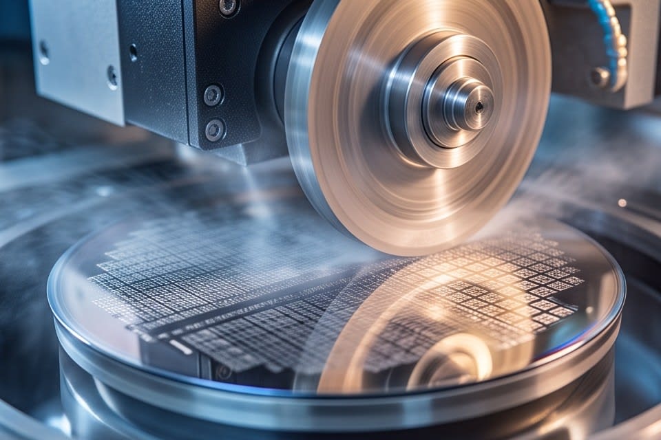
    A semiconductor wafer rotating while being precision ground by a diamond wheel

    The Two-Step Structure and Tolerance Standards of Precision Grinding

    To understand the tolerance level required by precision grinding, a sense of proportion is more important than the numbers themselves. The allowable tolerance required in grinding for semiconductor manufacturing equipment is about ±2.54μm(microns), which is only a few dozenths of the thickness of a human hair, considering that human hair is about 70 to 100μm thick.

    To reliably achieve this level of precision, commercial grinding systems operate two process stages in sequence.

    • Coarse grinding stage: Rapidly removes material at a speed of about 5μm per second.
    • Fine grinding stage: Reduces the speed to 1μm per second or less to secure surface roughness and thickness uniformity.

    Reducing speed is the core principle for increasing precision, and how precisely the transition point and conditions between the two stages are controlled is the key factor that determines final yield. Equipment configuration that combines a diamond wheel with a high-precision stage is the core hardware that reliably supports this transition process, and the completeness of equipment design is directly revealed under conditions that must satisfy both fine tolerance control and repeatable reproducibility.

    Precisely processed semiconductor packages arranged on a tray

    How PKG Grinder Responds to On-Site Conditions

    When introducing grinding equipment at an AI semiconductor packaging site, the first practical question is “which package types can it support”. In many cases, a single production line must handle multiple packages at the same time, including FCBGA, WLCSP, and QFN/DFN(Quad Flat No Lead), while the target thickness required by customers differs by product.

    Huvics PKG Grinder is designed for these on-site conditions with Full Auto A/B types and Manual type options, allowing flexible selection according to the automation level of the production line and the characteristics of the product. Processing uniformly and precisely to the thickness customers require is not simply a matter of equipment specifications. It means the equipment must allow settings that reflect actual process conditions and package structures.

    The requirement to maintain stable yield even during high-speed processes in manufacturing sites that handle ultra-precision components, such as camera modules or autonomous driving sensors, directly shows how important repeatable reproducibility and in-process consistency are for equipment. As stacked structures become more complex and target thickness becomes thinner, the range of precision that grinding equipment must handle also expands. This is where the significance of PKG Grinder in this process becomes clear.

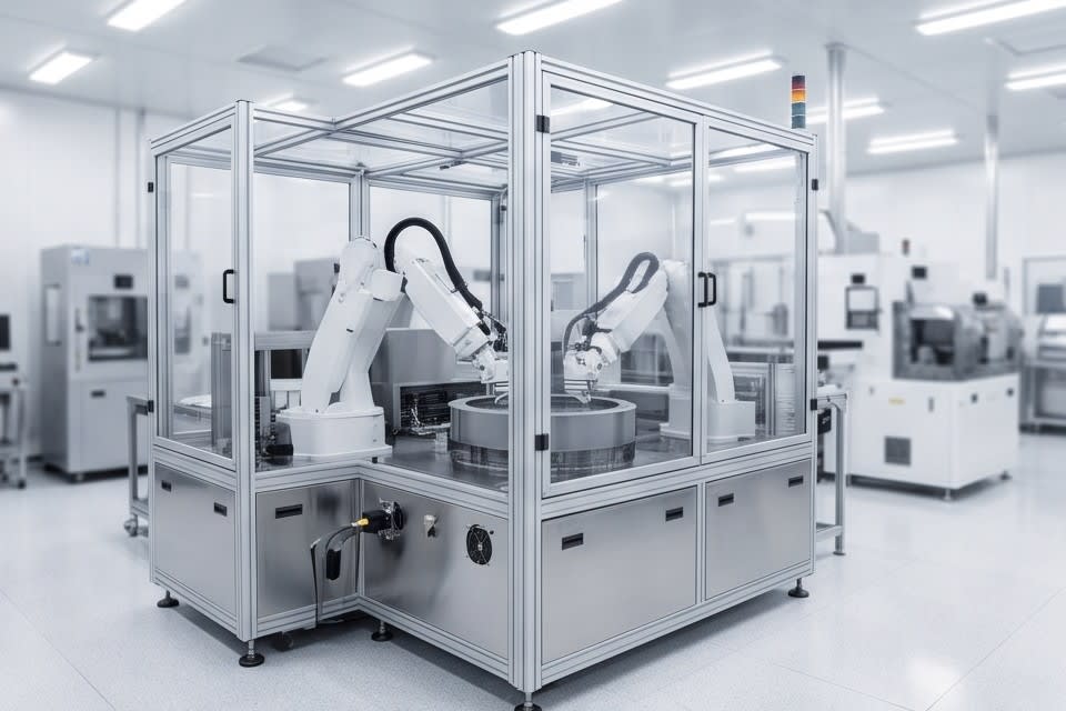
    Exterior of an automated grinding system installed in a cleanroom environment

    The complexity of stacked structures required by AI semiconductors has transformed the grinding process from a simple post-processing step into the starting point of quality. The ability to repeatedly achieve micron-level tolerances ultimately shows where the reliability and yield of the entire package are determined. As thickness targets become thinner and the number of stacked layers increases, the demand for grinding precision will continue to rise.


    Huvics is an advanced technology company that develops and manufactures automation equipment and
    production systems across the semiconductor, LED, Mobile, and Cosmetic industries.
    With top-level talent and continuous technological innovation, we support customers in improving productivity and
    securing quality competitiveness.

    Huvics Contact Information

    Phone: 031-374-8285
    Email: cdpark@huvics.com
    Huvics Inquiry

  • Complete Overview of Why Thickness Variation and Contamination Control Determine Semiconductor Yield

    Complete Overview of Why Thickness Variation and Contamination Control Determine Semiconductor Yield

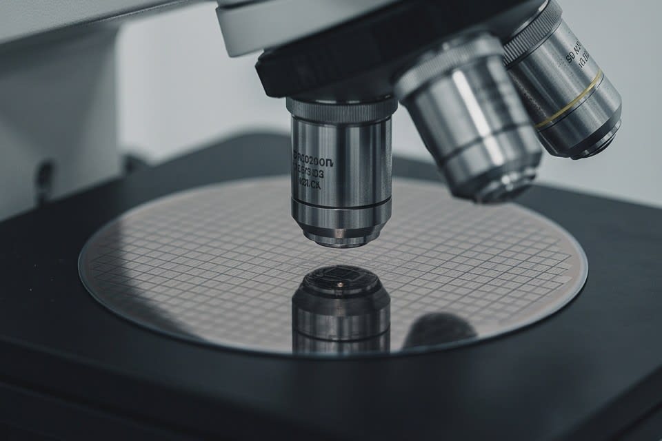
    A semiconductor wafer under a microscope shows the management of minute thickness variation and contamination particles.

    When I first took a close look at a semiconductor package process site, the customers I met all said something similar. “We changed the equipment and the materials, but we still do not know why defects are not decreasing.” What we commonly found at those sites was an issue that was hard to see with the naked eye: micron-level thickness variation and contamination particles left between process steps. Processes that appeared normal on the surface were quietly reducing yield at each stage as they accumulated and connected.

    A wafer with numerous dies arranged in a regular pattern visualizes precise thickness control in the stacking process.

    Why thickness variation determines yield

    AI semiconductors and high-performance memory semiconductors improve performance by vertically stacking dozens of chips. In this structure, if the thickness of each die is not uniform, alignment shifts during stacking, stress concentrates at the bonding area, and errors eventually occur in electrical signal transmission.

    According to analysis by Applied Materials, today’s HBM dies have become about one twenty-fifth the thickness of conventional DRAM, making them highly vulnerable to stress, warpage, and deformation. In addition, research published by ASME clearly shows that thickness variation and alignment mismatch worsen performance variation in HBM multi-layer stacking.

    As the number of stacked layers increases from 12 to 16 or more, these mechanical issues become intertwined in complex ways, increasing the risk of bonding defects and yield loss. Ultimately, package thickness control is not simply a dimensional matter but a key variable that determines the electrical performance and reliability of a product. As stacking increases, variation accumulates with it, and that error appears directly in the final yield. This is exactly why micron-level precision is required, and this trend becomes even clearer as next-generation packaging technology advances.

    A precision grinding wheel uniformly processes the surface of a semiconductor package.

    The direction of yield is set in the grinding stage

    PKG Grinder combines a high-precision stage with a diamond wheel to uniformly grind various packages such as FCBGA, WLCSP, QFN, and DFN to the customer-required thickness at the micron level. The key challenge this equipment addresses is achieving both speed and precision at the same time.

    Even in high-speed processes, thickness variation must be minimized to maintain yield, and the same level of precision must be guaranteed even when package types change to secure the stability of the entire production line. Since it supports both fully automated and manual operation, it can flexibly respond from low-volume, high-mix production to high-volume continuous processes.

    The grinding process is positioned to determine the quality of subsequent stacking and bonding in advance. Only dies with uniform thickness enable accurate alignment and stable bonding in the next process. The key point of this process is that yield is not created in the assembly stage, but its direction is already set in the grinding stage.

    A precision cleaning process removes contaminants by spraying streams of water onto the package surface.

    Contamination control that connects every process stage

    Process continuity from lamination to UV curing

    If thickness control is an issue before stacking, contamination control throughout the entire process is another axis of equal importance. In semiconductor package manufacturing, a process that connects lamination, tape mounting, and UV curing into one flow must consistently maintain adhesive strength and alignment accuracy between each step. If the process is interrupted or conditions change, quality variation occurs at that point.

    Multi-stage cleaning and static electricity suppression

    The same applies to the cleaning process. A multi-stage cleaning method that sequentially applies microbubbles, water jets, and air knives removes surface contamination particles step by step, while also implementing a principle that suppresses particle reattachment caused by static electricity between stages. To apply the same cleaning standards to components with different shapes and materials, such as camera modules, sensors, VCM motors, and trays, process conditions must be finely adjusted.

    In a reality where a single particle can be judged as a defect in the final inspection, cleaning is not the final finishing step but the point where quality begins. The Huvics Cleaner System integrates even oven drying functions to block additional contamination risks caused by residual moisture after cleaning. The fact that yield stability is maintained across the entire process only when contamination is controlled at every connection point is confirmed in actual production sites.

    A semiconductor packaging process site with complex equipment arrangements symbolizes process continuity.

    The frustration customers first expressed, the question “Why does it still not work after changing everything,” was ultimately answered in places that are not visible. Micron-level thickness variation, a single particle left between processes. Semiconductor quality control is not about replacing visible equipment, but about building precision at every connection point between processes. From grinding to cleaning, yield finally appears as a number when that flow is maintained consistently.


    Huvics is an advanced technology company that develops and manufactures automation equipment and
    production systems across the semiconductor, LED, Mobile, and Cosmetic industries.
    With top talent and continuous technological innovation, we support customers in improving productivity and
    securing quality competitiveness.

    Huvics Contact Information

    Phone: 031-374-8285
    Email: cdpark@huvics.com
    Contact Huvics

  • 3 Reasons Why Thickness Uniformity Determines Yield in 3D Stacked Packaging

    3 Reasons Why Thickness Uniformity Determines Yield in 3D Stacked Packaging

    A 3D stacked packaging structure with vertically thinned semiconductor chips precisely aligned in layers.

    According to recent reports, demand for AI semiconductors and high-performance memory is rising rapidly, further increasing the required precision of semiconductor packaging processes. As 3D stacked packaging, which improves performance by stacking chips vertically, emerges as a key technology, micron-level thickness control is becoming a critical factor that determines yield and reliability on the manufacturing floor. This shift presents a direct challenge to everyone involved in designing or operating semiconductor packaging processes.

    Semiconductor chips precisely stacked vertically while maintaining uniform thickness.

    Why Thickness Uniformity Matters in Stacked Packaging

    Stacking chips also means stacking tolerances. In 3D IC stacked structures, wafers must be processed from a thickness of about 780μm down to less than 10μm. If thickness is not uniform during this process, the thermo-mechanical reliability of the entire chip after stacking drops sharply. When a thinned wafer is uneven, stress is distributed unevenly across the bonding surface, which can lead to cracks or interlayer separation under long-term operating conditions.

    The same applies when external particles become trapped between wafers during stacking. A single particle can create a localized thickness variation, and that variation can cause delamination and interlayer separation, reducing bonding quality and yield at the same time. For this reason, controlling the total thickness variation of the wafer, TTV, to 1μm or less has become an industry benchmark in ultra-precision grinding processes.

    Looking only at the numbers, the requirement may seem simple. In actual mass production, however, consistently meeting this standard is an entirely different challenge. Even within a single wafer, thickness can vary depending on location, and equipment vibration, temperature changes, and subtle differences in grinding speed all affect TTV. In the end, the success of stacked packaging depends on how uniformly the wafer can be ground, making precision the decisive factor.

    A mechanical process in which a diamond wheel directly contacts the semiconductor wafer surface for precision grinding.

    How Mechanical Grinding Achieves Thickness Uniformity

    Two main methods are used to secure thickness uniformity: mechanical grinding and CMP, chemical mechanical polishing. CMP planarizes the surface by using chemical reactions and mechanical friction at the same time, while mechanical grinding directly removes material from the wafer using a diamond wheel, allowing it to reach the same target thickness in less time.

    The speed advantage is clear, but fast grinding alone is not enough. The process must also include control capabilities that detect thickness variation in real time and correct it immediately during grinding. Research showing that a real-time closed-loop TTV control system can reduce TTV by up to 72.2% within a single grinding process supports this point.

    Huvics PKG Grinder is based on this mechanical grinding technology and combines a high-precision stage with a diamond wheel to achieve micron-level precision processing. Since thickness targets and tolerances differ by package type, such as FCBGA, WLCSP, and QFN/DFN, it is important for equipment to be configured to respond flexibly to diverse package specifications. With both Full Auto and Manual types available, it can be selectively applied according to the automation level of the production line. The grinding process is implemented in a way that satisfies both precision and flexibility at the same time.

    A semiconductor chip array aligned with consistent spacing and shape through micron-level tolerance control.

    The Meaning of Thickness Uniformity in AI and High-Performance Memory Production

    As demand for AI accelerators and high-bandwidth memory, HBM, grows rapidly, the requirements for packaging processes are also rising. In particular, AI packaging environments have shown that micron-level dielectric thickness variation can reduce system efficiency, data transmission bandwidth, and beamforming accuracy to a measurable degree. No matter how precisely circuits are designed, thickness variation in the packaging process can prevent the final product from reaching its intended performance targets.

    In this context, the idea that performance is completed not in design but in process becomes especially clear. For this reason, in production sites for AI semiconductors and high-performance memory, the key selection criterion is not simply the ability to grind thinly, but equipment reliability that can maintain stable thickness uniformity even during high-speed processing. PKG Grinder is designed to maintain stable quality under high-speed process conditions and achieve high yield, responding to the needs of production environments that require both yield and process stability. As stacked packaging technology becomes a key factor determining next-generation semiconductor performance, technological competition around grinding process precision is becoming even more intense.

    Automated semiconductor manufacturing equipment installed in a cleanroom environment where ultra-precision grinding processes are performed.

    Ultimately, the quality of stacked packaging is determined not by the design drawing, but by the precision of the grinding process. In a structure where the ability to control thickness uniformity to 1μm or less determines both yield and reliability, choosing process equipment is not simply an investment in facilities, but a decision that shapes product competitiveness. The packaging precision standards required in the AI semiconductor era are continuing to rise, and consistently meeting those standards on actual mass production lines remains the key challenge ahead.


    Huvics is an advanced technology company that develops and manufactures automation equipment and
    production systems across the semiconductor, LED, Mobile, and Cosmetic industries.
    With top talent and continuous technological innovation, we support customers in improving productivity and
    securing quality competitiveness.

    Huvics Contact

    Phone: 031-374-8285
    Email: cdpark@huvics.com

    Huvics Inquiry

  • 3 Process Points That Prevent Semiconductor Defects – Key Summary of Grinding, Lamination, and Cleaning

    3 Process Points That Prevent Semiconductor Defects – Key Summary of Grinding, Lamination, and Cleaning

    A completed chip semiconductor packaging component after vertical stacking and lead frame alignment

    If defects are found in parts after cleaning, the loss has already started somewhere in the process. Thickness variation in the grinding stage, uneven adhesion in the tape attachment process, contamination residue remaining after cleaning — if even one of these three issues is overlooked, yield loss and rework costs can grow rapidly. The later a problem appears in the downstream process, the more correction costs increase exponentially, and delayed delivery can even undermine customer trust.

    A smoothly processed circular wafer placed on equipment with tolerances of less than 1 micron

    Thickness Uniformity in the Grinding Process Determines Yield

    In the semiconductor packaging process, thickness uniformity is one of the most sensitive variables that determines yield. Modern package structures such as WLCSP wafer level chip scale package, FCBGA, and QFN are based on vertical chip stacking, and if the thickness after grinding is even slightly uneven, stacking chips on top becomes impossible.

    According to analysis by AE Research, the thickness uniformity tolerance required in semiconductor grinding processes is less than 1 micron, and chips outside this standard immediately lead to defects in the stacking process. This is why micron level precision grinding using diamond wheels is not simply a machining technology, but a prerequisite for package reliability. To maintain this level of tolerance consistently even in high speed processes, stage precision and consistent grinding conditions must both be secured. Keeping thickness variation within the allowable range is the key to high yield production.

    A lamination film attachment process applying tape evenly to a wafer surface with a roller

    Integrated Lamination Processes Prevent Error Accumulation

    The more a process is divided into multiple stages, the more errors accumulate between each stage. When tape attachment, UV curing, and expanding are performed on separate equipment, alignment can shift or adhesion conditions can vary during transfer between processes.

    The laminator system from Huvics structurally prevents this issue by integrating key processes from the expander to UV curing within a single system. In the UV curing stage, uniform irradiation intensity is especially important. Uneven UV irradiation causes film shrinkage and adhesion variation, increasing the risk of damage in the subsequent chip separation process. In contrast, when UV curing is performed under controlled conditions, tape adhesion weakens predictably, allowing chips to be separated without damage.

    A UV curing system that can selectively apply lamp and LED methods provides the flexibility to respond according to product type and production volume. Connecting processes into one continuous flow and reducing the number of transfers is itself implemented as a way to secure both shorter takt time and process stability.

    High pressure water jets sprayed from nozzles to remove foreign particles from the surface of semiconductor components

    The Cleaning Process Is the Final Gateway to Quality

    No matter how precise the machining and attachment processes are, final quality becomes unstable if contaminants remaining on the surface are not removed. In camera module manufacturing sites, if residual flux and contamination particles generated during the reflow process after CSP assembly are not removed through cleaning, ionic residues cause corrosion and directly affect module performance.

    In production environments that handle components with diverse shapes and materials, such as VCM motors, image sensors, and trays, a single cleaning method makes it difficult to respond to all types of contamination. The cleaner system from Huvics removes surface contamination particles step by step through a multi stage cleaning method that combines micro bubbles, water jet, and air knife, and it also includes an oven drying function to remove residual moisture after cleaning.

    Full auto and manual methods can be selected, allowing flexible application depending on the line configuration. In automated configurations, worker intervention between processes is minimized, reducing the risk of contamination reattachment. In the field, results show that as the defect rate in the cleaning stage decreases, the downstream rework rate also drops.

    A continuous process line where semiconductor components are transferred along a conveyor belt in an automated system

    Micron level precision in the grinding process, an integrated flow in the lamination process, and multi stage contamination removal in the cleaning process — these three elements are not separate technologies, but one connected line of defense against semiconductor defects. Weakness in any one stage is transferred as a burden to the next stage, and the structure in which it is ultimately confirmed as a defect in final inspection will inevitably repeat unless the entire process is designed with precision. Controlling variation at each point in the process is a far more cost effective way to protect quality than tracing the cause after a defect occurs.


    Huvics is an advanced technology company that develops and manufactures automation equipment and
    production systems across the semiconductor, LED, Mobile, and Cosmetic industries.
    With top talent and continuous technological innovation, we support customer productivity improvement and
    quality competitiveness.

    Huvics Contact

    Phone: 031-374-8285
    Email: cdpark@huvics.com

    Contact Huvics

  • Thickness Variations That Disrupt Semiconductor Package Yield, Explained Through Grinding and Lamination Field Applications

    Thickness Variations That Disrupt Semiconductor Package Yield, Explained Through Grinding and Lamination Field Applications

    A semiconductor manufacturing site where an operator inspects micron-level errors under a microscope

    Semiconductor quality management is, in simple terms, a matter of how precisely allowable tolerances are controlled at each stage of the process. Invisible micron-level variations determine the reliability of the finished product, and this issue becomes even more apparent in advanced package structures where chips are stacked in multiple layers. The moment terms such as ‘thickness uniformity’ or ‘flatness’ come up on the manufacturing floor, they are not simply about dimensions but about issues that affect overall yield and reliability.

    Cross-sectional structure of an advanced semiconductor package with vertically stacked dies

    Why Thickness Variation Undermines Package Reliability

    Stacking chips also means, in a sense, stacking tolerances. In structures such as AI semiconductors or high-performance memory, where dozens of dies are vertically stacked, thickness variation in each layer accumulates and compromises the flatness of the entire package.

    The international semiconductor standard JEDEC defines the maximum allowable warpage for large flip chip packages as 200μm, and cases have been reported where warpage deformation reaches 87μm under reflow temperature conditions. Once this value exceeds the threshold, signal integrity becomes unstable and interlayer bonding defects can occur.

    In high-bandwidth memory, it is already widely recognized across the industry that thickness variation alone in the interposer manufacturing process can cause impedance deviation. If thickness is not uniform, electrical performance cannot be uniform either, and the principle that an uneven package cannot be reliable has become the starting point of advanced package design.

    A process that machines the surface of a semiconductor wafer with a high-speed rotating grinding wheel

    How a Reference Surface Is Created in the Grinding Process

    PKG Grinder is equipment that directly addresses this issue. Regardless of package type, including FCBGA, WLCSP, QFN, DFN, and Solar Cell, it performs micron-level precision grinding to achieve the target thickness required by the customer.

    This machining method, implemented through the combination of a high-precision stage and a diamond wheel, maintains uniform results even in high-speed processes without reducing yield, contrary to the common belief that speed and precision are usually inversely related. Because it supports both Full Auto and Manual configurations, it can respond flexibly to everything from low-volume, high-mix lines to mass production systems.

    Grinding is not simply a task of reducing thickness. It is the process of creating a reference surface on which all subsequent processes depend. Since the uniformity and flatness of that reference surface determine the reliability of the final package, precision control in the grinding stage is the practical key to securing quality.

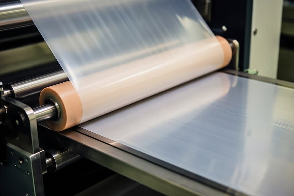
    A semiconductor package film lamination process fed through rollers

    The Impact of the Lamination Process on Adhesion Reliability

    Thickness uniformity issues do not occur only in the grinding process. If film thickness is formed unevenly during the ABF lamination process, the electrical performance of subsequent circuits varies from layer to layer and reliability decreases.

    Lamination may appear to be a simple process of attaching film, but even a slight imbalance in the combination of temperature and pressure can cause delamination defects or uneven adhesion strength. According to research findings, cases have been reported where delamination defects decreased by up to 67% when optimized lamination parameters were applied.

    Huvics’ laminator system features an integrated process structure that connects everything from Expander to UV Curing in a single flow, and secures both adhesion strength and process stability through Lamp and LED type UV curing systems. With Semi Auto and Manual options, it can support various product specifications and production requirements, and it is designed to reduce takt time by simplifying process steps.

    Field applications continue to confirm that overall package quality stability is achieved only when the two processes, setting the reference surface through grinding and building layers through lamination, are each precisely controlled.

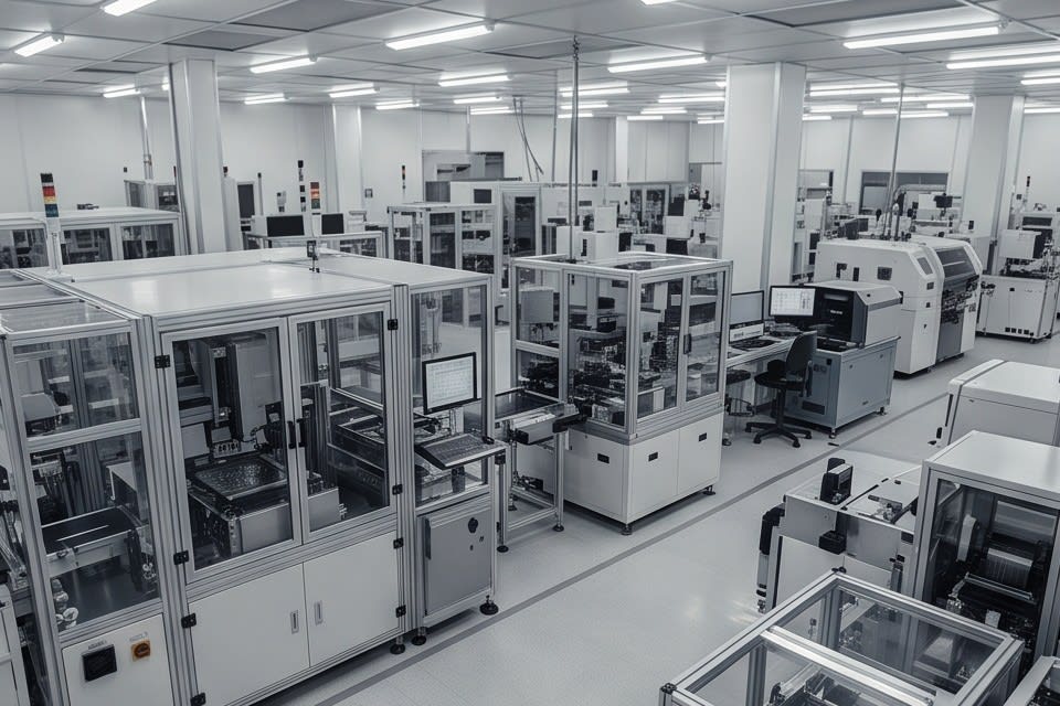
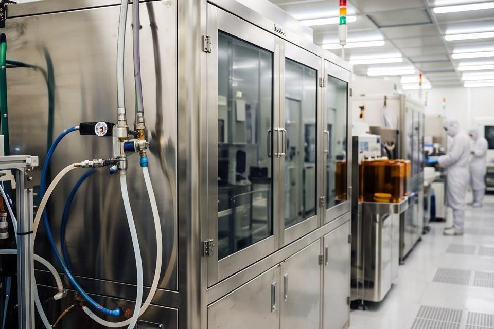
    View of semiconductor manufacturing equipment in a cleanroom where precise process control is performed

    Semiconductor package quality cannot be guaranteed by the completeness of a single process alone. Reliable results emerge only when the uniform reference surface created in the grinding stage works together with precise temperature and pressure control in the lamination stage. Managing micron-level variation is ultimately a matter of designing the entire process as one connected flow, and the essence of quality management lies in how tightly the allowable tolerance of each stage can be narrowed within that flow.


    Huvics is an advanced technology company that develops and manufactures automation equipment and
    production systems across the semiconductor, LED, Mobile, and Cosmetic industries.
    With top talent and continuous technological innovation, we support customers in improving productivity and
    securing quality competitiveness.

    Huvics Contact

    Phone: 031-374-8285
    Email: cdpark@huvics.com

    Huvics Inquiry

  • Why Semiconductor Cleaning and Grinding Processes Determine Yield and Profitability

    Why Semiconductor Cleaning and Grinding Processes Determine Yield and Profitability

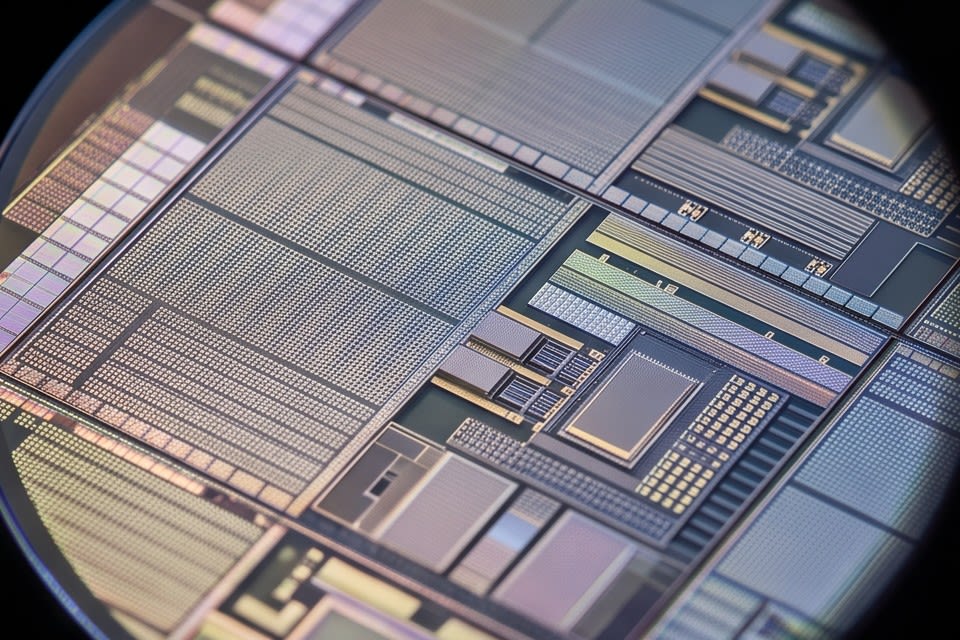
    Microscopic circuit patterns on a semiconductor wafer observed through a microscope

    If you work in semiconductor process management, you have probably experienced this at least once. The line is running normally, the equipment shows no issues, and the recipe has not changed, yet defective products quietly begin to increase. When you trace the process backward to find the culprit, what you eventually encounter is a microscopic contamination particle that is barely visible. It may feel unfair that a single micron-scale speck of dust can shake the yield graph, but this is the reality. Today, we will talk about cleaning equipment that can help reduce that frustration, even if only a little.

    Interior view of a cleanroom with precision electronic components and measurement equipment

    Why the Cleaning Process Is the Starting Point of Yield

    There are many variables that determine yield in semiconductor and electronic component manufacturing, but the cleaning process carries far more weight than many people expect. Contamination particles left on the product surface can lead to pattern defects or bonding failures in subsequent processes, and problems that occur at this stage often become visible only during final inspection. By the time defects start to appear, the product has already passed through several process steps.

    Industry cases have reported that adopting contamination control solutions can reduce defect rates by up to 45%, which shows that cleaning is not a final stage of quality control, but closer to the starting point of yield. The key here is not simply washing particles away, but designing the process to suppress static electricity so that removed particles do not adhere to the surface again. Static electricity generated immediately after cleaning can cause removed particles to reattach, and without controlling it, the cleaning process itself can lose its meaning.

    In the end, the quality of a cleaning process is evaluated by two factors: how cleanly the surface was washed and how well that cleaned condition was maintained. Equipment design that satisfies both conditions at the same time is becoming a practical dividing line between yield and profitability.

    Automated manufacturing process line composed of robotic arms and a conveyor system

    Structure and Cost Effect of a Multi-Stage Cleaning and Drying System

    The method that implements these two conditions within a single process flow is a multi-stage cleaning and drying system. A structure that applies Micro Bubble, Water Jet, and Air Knife in sequence creates complementary steps that physically suspend contamination particles, push them away with strong water flow, and remove residues with high-speed airflow. When Oven Dry functionality is integrated, cleaning and drying are completed within one line after washing, reducing the possibility of recontamination during transfer between processes.

    Huvics Cleaner System supports both Full Auto and Manual methods so this structure can be applied to product groups with diverse shapes and materials, including camera modules, sensors, VCM motors, and trays. In automated operation, the system automatically controls chemical input according to process conditions. According to analysis by Modutek, combining automated dosing with a chemical life extension design can reduce chemical consumption by up to 80%. This directly leads to lower material costs and reduced waste liquid treatment costs, making it a factor that can substantially change the operating cost structure compared with equipment investment.

    This is why cleaning equipment should be evaluated not only by cleaning performance, but also by its level of automation and chemical management method. The effect of multi-stage cleaning is proven by the defect rate figures confirmed at the end of the process, but the key point is that its cost effect accumulates across overall operations.

    A robotic arm handling a precision wafer and loading it into processing equipment

    The Link Between Package Thickness Uniformity and Profitability

    If the cleaning process deals with surface contamination, package thickness precision is another dimension of yield control. As demand for AI semiconductors and high-performance memory increases, structures that stack chips vertically are becoming common, and processes that grind wafers extremely thin have become essential for this purpose. According to technical materials from Vitrek, DRAM memory wafers are thinned to about 50 microns for high-density stacking, and the thickness variation that occurs during this process reaches the range of several microns.

    If this variation exceeds the allowable range, the flatness of the entire package after stacking collapses, which can lead to electrical connection failures or heat dissipation problems. Huvics PKG Grinder is equipment that combines a high-precision stage with a diamond wheel to grind thickness uniformly at the micron level, and it supports various package types such as FCBGA, WLCSP, QFN, and DFN. Maintaining thickness uniformity even during high-speed processing is the core design objective of this equipment, and this directly improves stacking yield.

    When yield increases, more good products can be secured with the same wafer input, which leads to lower unit production cost. The fact that one thickness variation can divide yield, and the difference in yield accumulates into a difference in profitability, quietly explains why ultra-precision processing equipment has become core infrastructure for manufacturing competitiveness.

    Semiconductor packages uniformly aligned on a tray

    Cleaning and grinding may seem like separate processes at first glance, but ultimately they move toward the same goal. Removing contamination, maintaining shape with precision, and ensuring that the result leads to the quality and profit of the final product. If even one process becomes loose, yield will not meet expectations no matter how precise the other processes are. The real reason for introducing automation equipment on the manufacturing floor is not convenience, but maintaining this chain of connection with stability.


    Huvics is an advanced technology company that develops and manufactures automation equipment and
    production systems across the semiconductor, LED, Mobile, and Cosmetic industries.
    With top talent and continuous technological innovation, Huvics supports improvements in customer productivity and
    the securing of quality competitiveness.

    Huvics Contact

    Phone: 031-374-8285
    Email: cdpark@huvics.com

    Huvics Inquiry

  • Why Semiconductor Packaging Yield Is Controlled in the Order of Grinding Cleaning Integrated Design

    Why Semiconductor Packaging Yield Is Controlled in the Order of Grinding Cleaning Integrated Design

    Wafers aligned at consistent intervals show the strict precision required in the packaging process.

    Semiconductor equipment experts commonly say that “the precision of the packaging process directly determines product reliability.” This means that even if the thickness deviation of a single chip is only a few micrometers, it directly affects the electrical characteristics and yield of the entire stacked structure. This is why process precision is discussed before simple production speed when talking about semiconductor automation equipment.

    Thin wafers stacked vertically in layers intuitively represent the 3D stacked structure of semiconductor packaging.

    Why thickness uniformity has become a key process variable

    Semiconductor packaging technology is rapidly shifting from single chip structures to 3D stacked structures in which dozens of chips are stacked vertically. AI semiconductors and high performance memory products are driving this trend, and the thickness precision required inside packages is becoming increasingly stringent.

    In 3D stacked structures, wafer thickness sometimes needs to be reduced from about 780μm to 10μm or less, and at this point, thickness uniformity becomes a key variable that determines whether design performance can be realized in practice. According to research published in ScienceDirect, the total thickness variation for a 300mm wafer must be achieved at 0.5μm or less to stably maintain the electrical characteristics of high performance memory devices.

    As the bonding area between chips becomes narrower and the number of stacked layers increases, a single thickness deviation can compromise the reliability of the entire package. The goal is not simply to make wafers thinner, but to make them uniformly thin. Building a process environment that meets this standard has become the starting point for introducing semiconductor automation equipment.

    A diamond wheel contacts the wafer surface and physically processes it while controlling thickness at the micron level.

    Precision in the grinding process and automation design

    In the grinding process, the diamond wheel removes the wafer surface at the micron level to control thickness. Surface roughness and material removal rate vary significantly depending on machining conditions. According to research results, in diamond wheel grinding, surface roughness is measured in the Ra 0.486~1.118μm range, and the material removal rate is measured at 555~1546μm/h. These figures show that the range varies widely depending on condition settings, which makes precise management of process parameters essential.

    Increasing grinding speed improves productivity, but it can create unwanted stress and dislocations inside the wafer, negatively affecting device performance and yield. How to balance fast removal with precise removal is the key criterion in equipment selection.

    This is where grinder systems configured as Full Auto and Manual Type attract attention. The Huvics PKG Grinder combines a high precision stage with a diamond wheel and is designed to secure stable quality even in high speed processes for various package types such as FCBGA, WLCSP, and QFN/DFN. The ability to choose between Full Auto and Manual depending on the production line configuration is also a factor that enables flexible response in sites where high mix low volume production and mass production coexist. Securing precision and productivity at the same time is the core of the automated grinding process.

    Liquid is sprayed onto the wafer surface through a precision nozzle to clean fine particles after the process.

    The role of cleaning and drying processes and integrated design

    The cleaning process is often considered a post process in semiconductor manufacturing, but in reality, it is performed repeatedly enough to account for about 30% of the entire front end process. A single fine particle left on the surface after grinding or stacking can become the source of defects in the next process step. For components with high precision requirements, such as camera modules, autonomous driving sensors, and VCM motors, the completeness of the cleaning process plays an even larger role in determining final quality.

    As the understanding spreads across production sites that a single cleaning method cannot effectively respond to various types of contamination, methods that combine multi step cleaning technologies such as micro bubbles, water jets, and air knives are gaining attention. The Huvics Cleaner System integrates oven drying with these multi step cleaning technologies to reduce the possibility of secondary contamination caused by residual moisture after cleaning.

    As particle removal efficiency improves, the defect rate decreases, and that result leads directly to final yield. The perspective of designing the cleaning process not as an independent step but within the flow of the overall automation equipment is becoming established, and this shift is significant in that it is redefining semiconductor production efficiency.

    Various automation equipment units are arranged in a row and connected as one yield management system on a production line.

    The competitiveness of semiconductor automation equipment ultimately depends on how precisely and consistently each process is connected. From the grinding process that controls thickness uniformity, to the automation system that precisely controls machining conditions, to multi step cleaning that removes fine contamination, these three process principles do not operate independently but work together as one yield management system. This is why integrated design between processes should be reviewed before the specifications of individual equipment when considering equipment introduction.


    Huvics is an advanced technology company that develops and manufactures automation equipment and
    production systems across the semiconductor, LED, Mobile, and Cosmetic industries.
    With top talent and continuous technological innovation, we support customer productivity improvement and
    quality competitiveness.

    Huvics Contact Information

    Phone: 031-374-8285
    Email: cdpark@huvics.com
    Huvics Inquiry