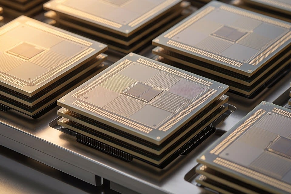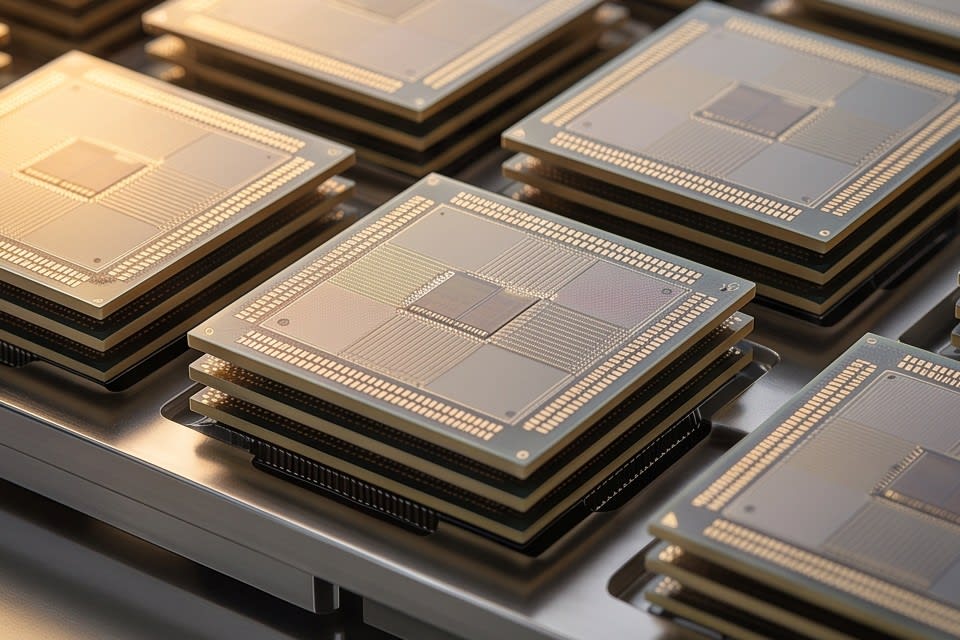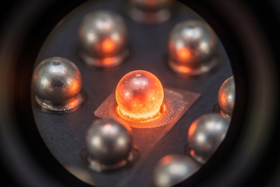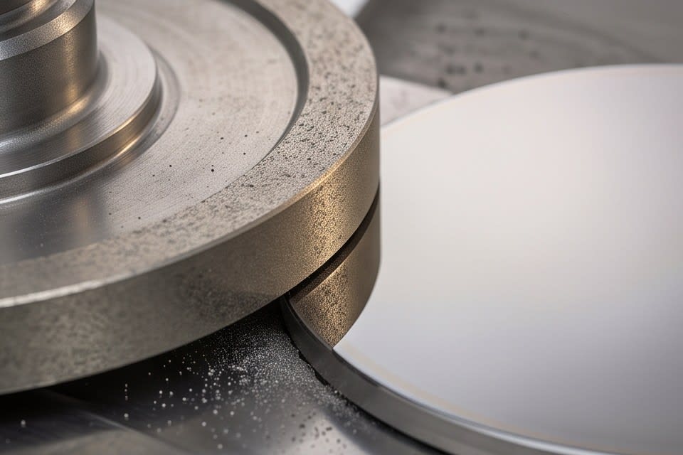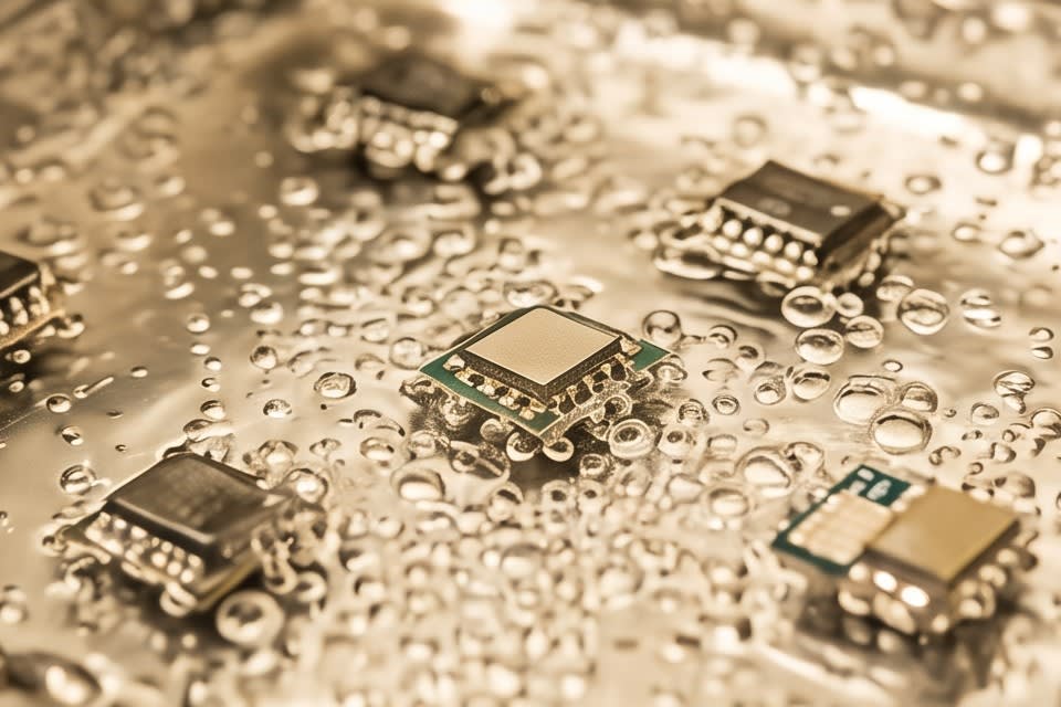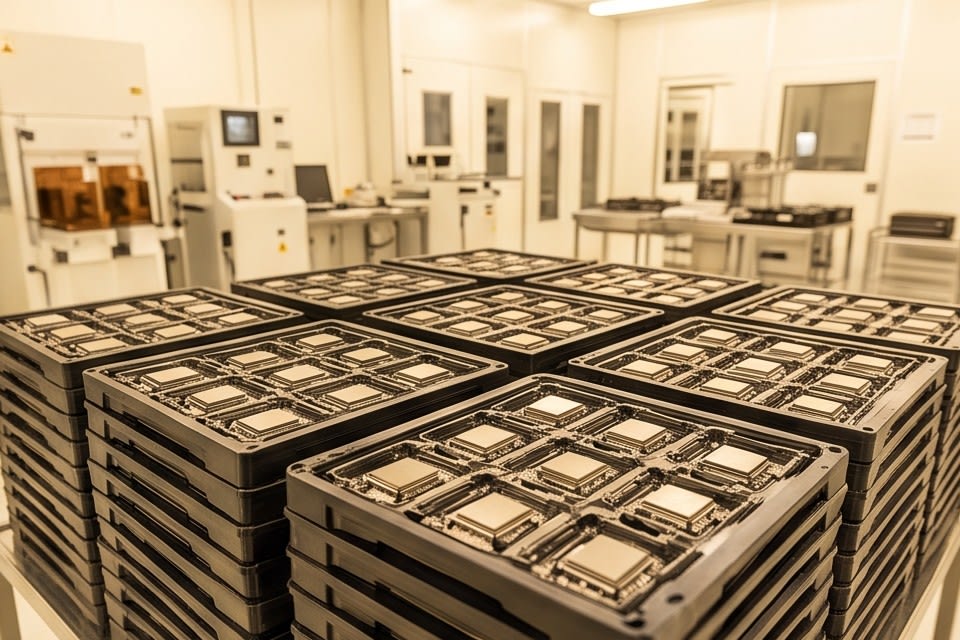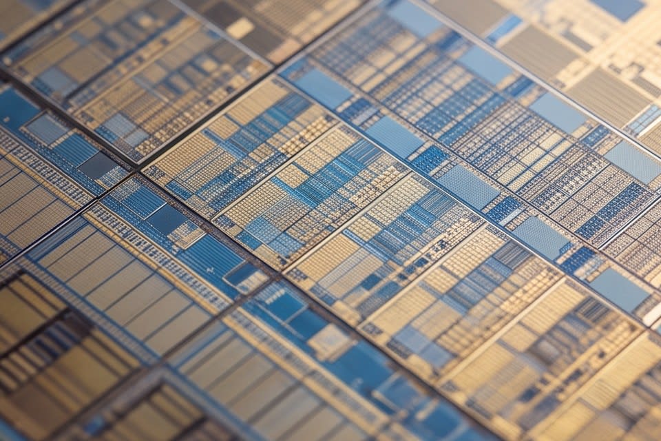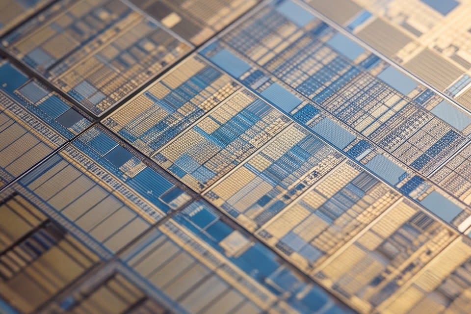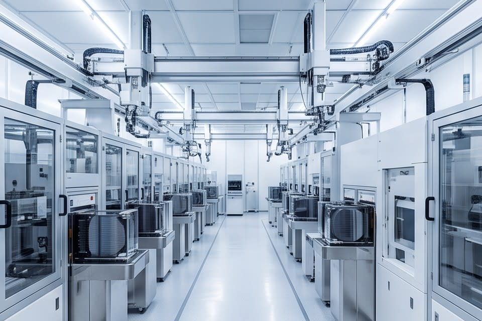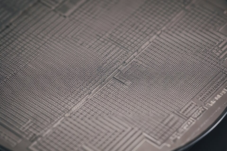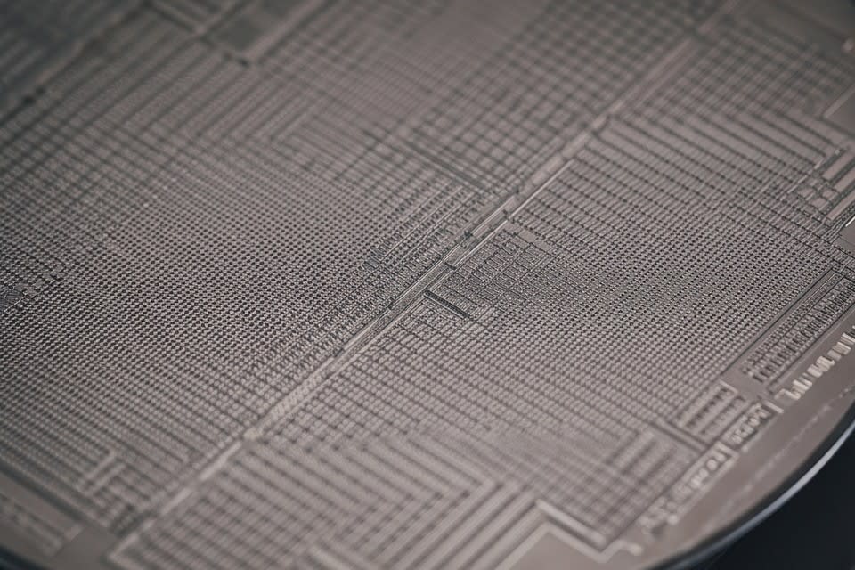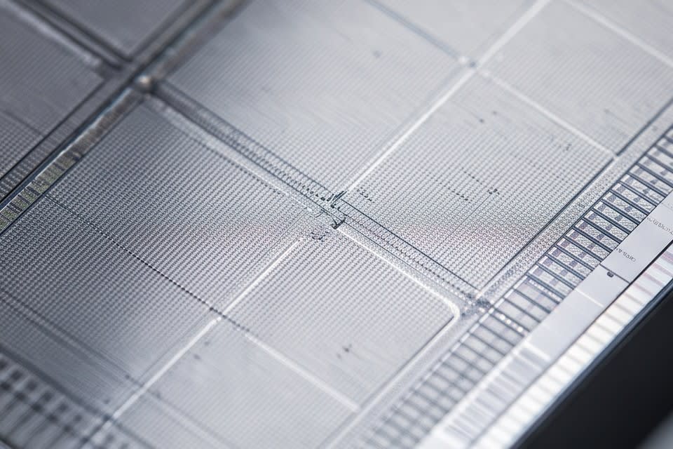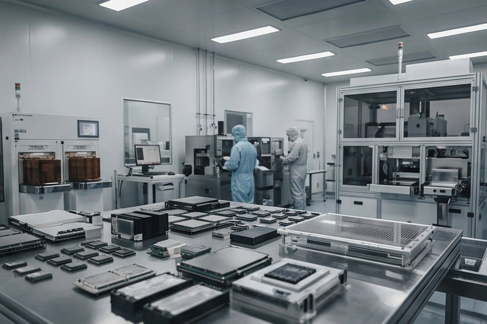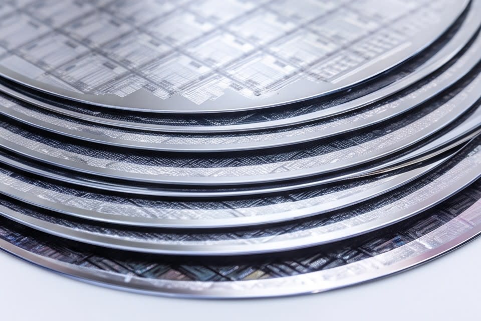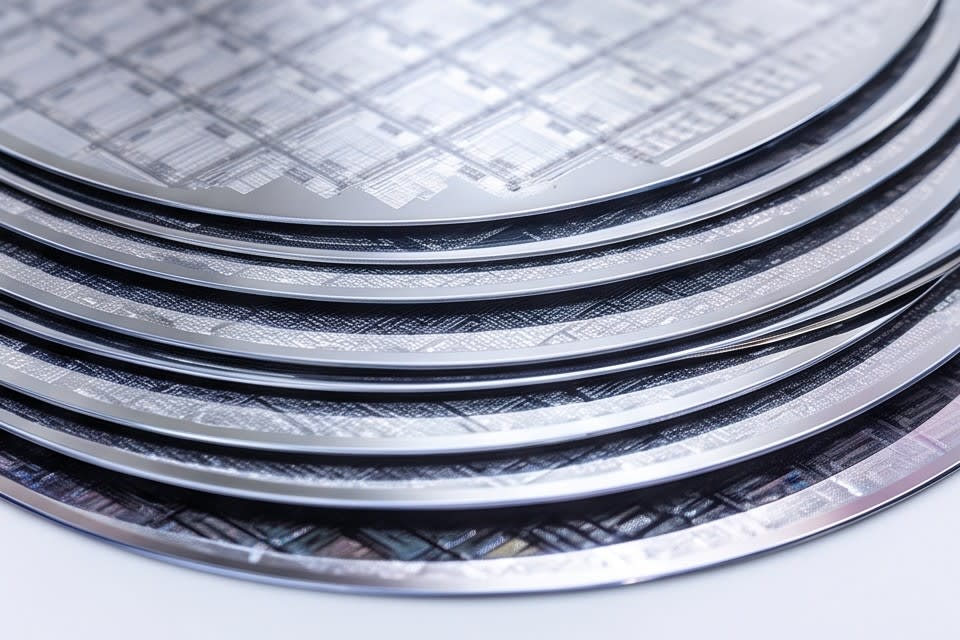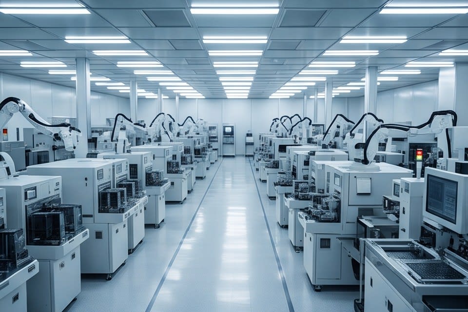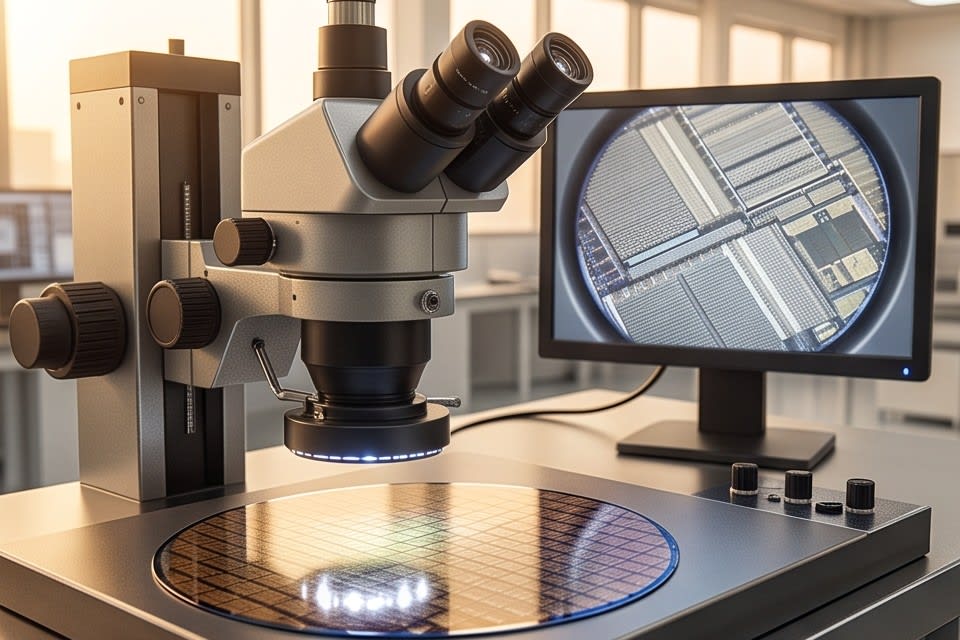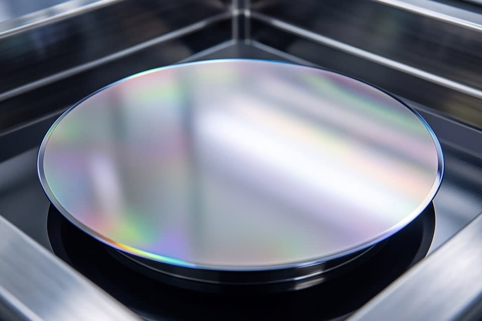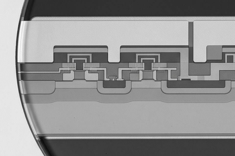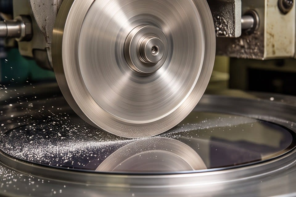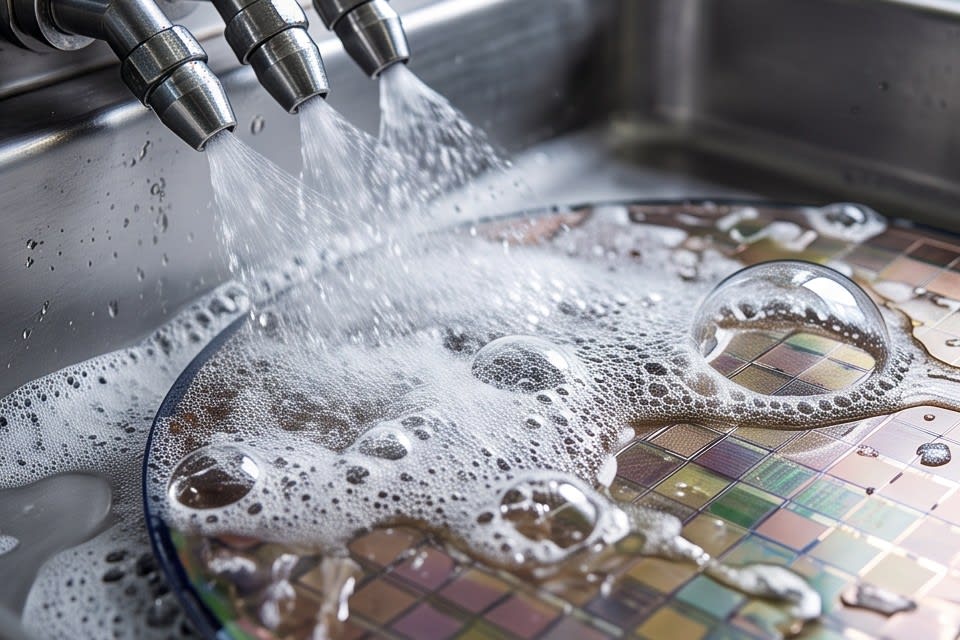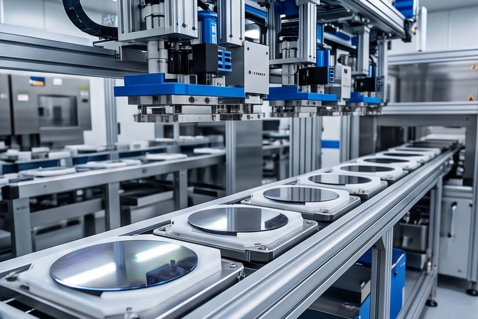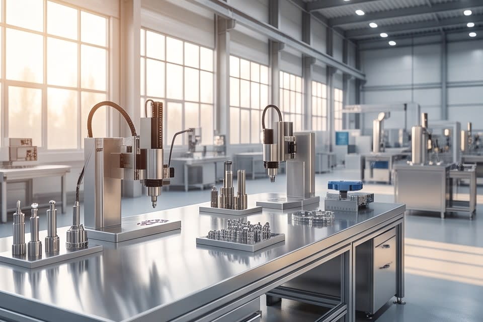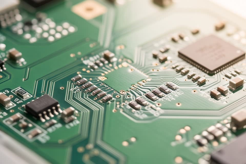
Cleaning processes in the electronic components industry have been gaining attention for quite some time. In the past, it was often enough to remove visible contaminants, but as semiconductor circuit line widths have narrowed to just a few nanometers, the standards themselves have changed. As process precision increases, the allowable level of contamination decreases, and the role required of cleaning technology continues to expand. Now that how precisely fine contaminant particles can be removed has become a key factor determining product reliability, the depth of cleaning technology has become the depth of competitiveness.
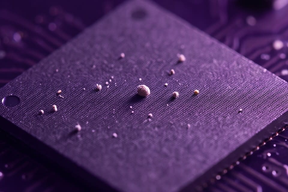
Why a Single Contaminant Particle Can Disrupt Overall Yield
In semiconductor processes, the impact of a single contaminant particle is far more critical than many might expect. According to data from the United States Patent and Trademark Office, even one particle measuring 0.01 micrometers can cause an entire chip to become defective if it comes into contact with a circuit. There is also analysis showing that in advanced processes at the 14 nanometer level, even a particle measuring 7.2 nanometers can ruin a single die.
As circuit line widths become narrower, the allowable contamination threshold also drops. Research in semiconductor manufacturing estimates that 75% of yield loss originates from contamination. This figure shows that the cleaning process is not simply about maintaining cleanliness, but is a core process directly linked to yield. Components with densely arranged fine patterns, such as MLCCs and FPCBs, are even more sensitive to surface contamination. As process environments become more precise, contamination control is becoming a prerequisite rather than an option across the industry.

How Ultrasonic Dispersion Technology Differs from Conventional Cleaning Methods
The limitations of conventional cleaning methods are structurally clear. Manual brushing or spray cleaning can be somewhat effective when component surfaces are broad and structures are simple. However, in cases such as high density substrates, where component spacing is narrow and there are many recessed areas, the cleaning solution may not reach surfaces uniformly, making it easy for contaminants to remain.
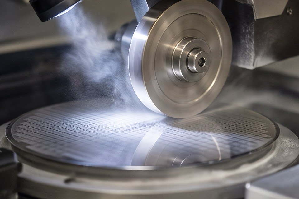
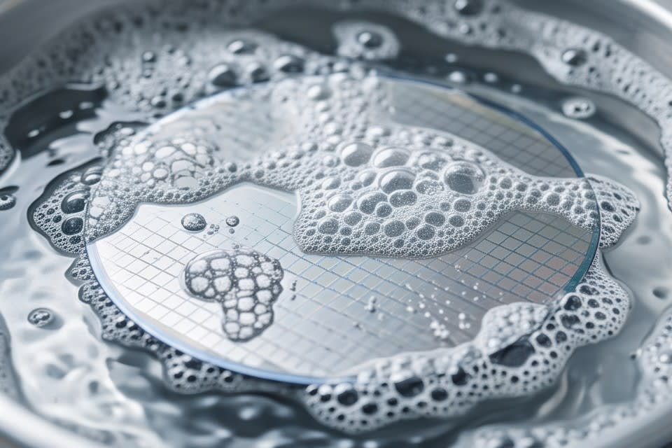
Ultrasonic cleaning approaches this problem in a different way. When high frequency sound waves of 20 kilohertz or higher pass through a liquid, countless microbubbles measuring 1 to 200 microns are created, and at the moment these bubbles collapse, pressure of up to about 20,000 psi is concentrated in a small area. Because contaminants are detached without physical contact, no scratches are left on component surfaces. This principle also allows the cleaning effect to be delivered uniformly into narrow gaps and complex internal shapes.
Huvics adds its proprietary dispersion control method to this ultrasonic technology, implementing a multi stage cleaning structure that combines Micro Bubble·Water Jet·Air Knife. Advancing the technology not only to remove contaminants but also to uniformly disperse material particles in a liquid phase is an approach that differs from conventional ultrasonic cleaning.
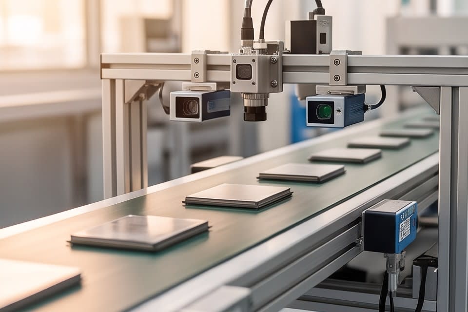
How Cleaning and Inspection Are Integrated into a Single Flow
If defects remain after cleaning is completed, the issue is discovered not in the cleaning stage, but in the inspection stage. However, when defects are found in the later part of the process, the materials and time already invested cannot be recovered. In environments such as MLCC or FPCB processes, where each component carries a high unit cost and production speed is fast, these losses can accumulate quickly.
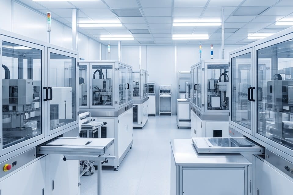
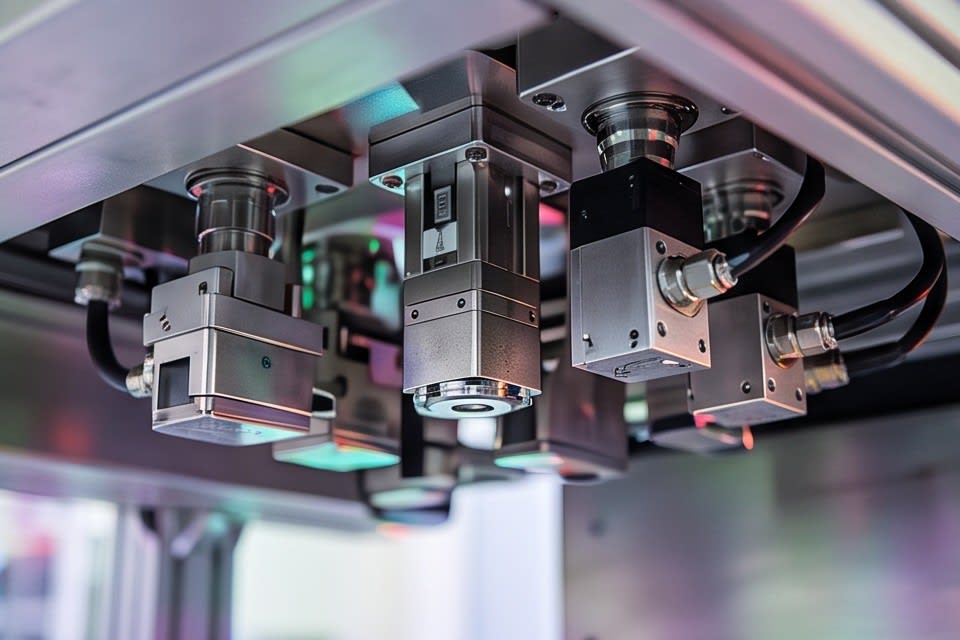
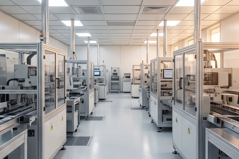
The integrated solution from Huvics enables ultrasonic dispersion technology and vision inspection algorithms to operate together within a single process. Because fine pattern defects are detected in real time while cleaning is being performed, defects can be identified in the early stage of the process. Cleaning conditions are optimized for various component types, including camera modules, sensors, VCM motors, and trays, and the drying process is handled continuously through the Oven Dry function.
When particle removal efficiency improves, the defect rate decreases, and when the defect rate decreases, final yield becomes stable. Integrating cleaning and inspection into a single flow rather than keeping them as separate processes is the key to reducing quality variability at the beginning of the process.
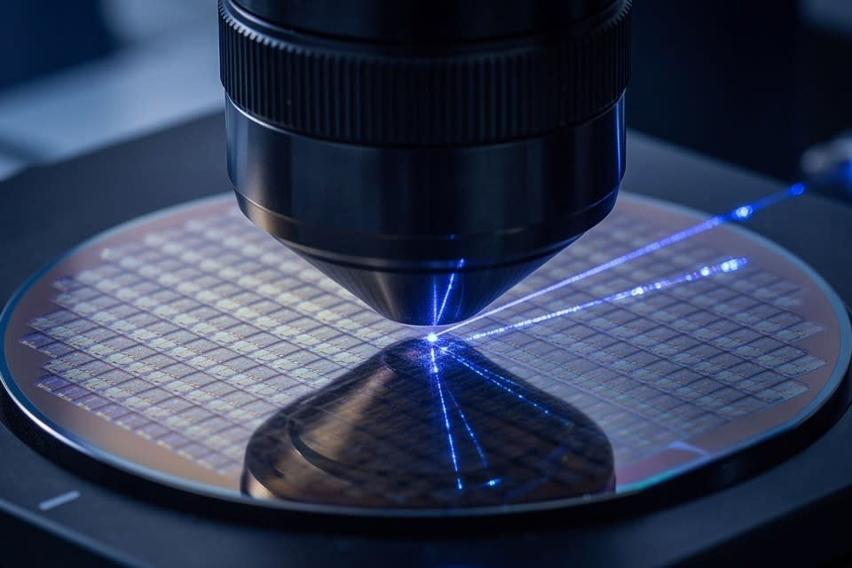
The trend toward higher process precision in semiconductors and advanced electronic components will not change going forward. In an environment where a single contaminant particle can disrupt overall yield, cleaning technology can no longer remain a simple post process. The method in which ultrasonic dispersion and real time vision inspection work together within a single process is one practical answer to this shift.
Huvics is an advanced technology company that develops and manufactures automation equipment and
production systems across the semiconductor, LED, Mobile, and Cosmetic industries.
With top talent and continuous technological innovation, we support customer productivity improvement and
quality competitiveness.
Huvics Contact
Phone: 031-374-8285
Email: cdpark@huvics.com