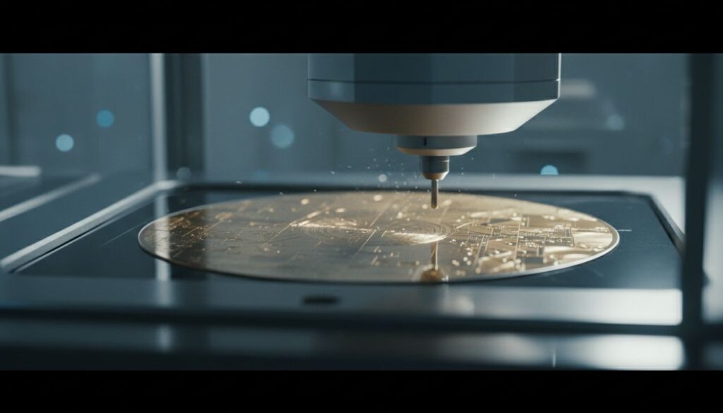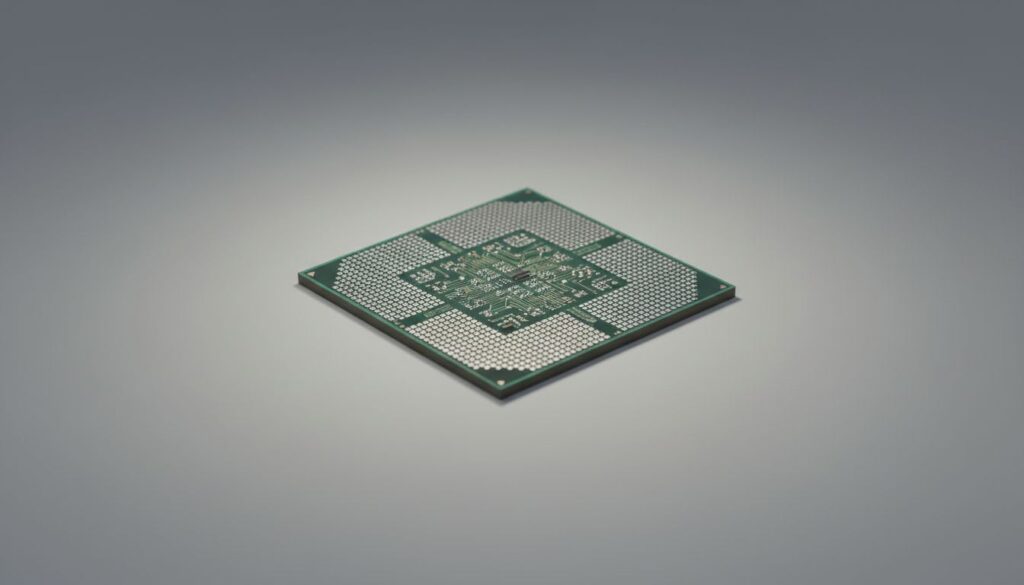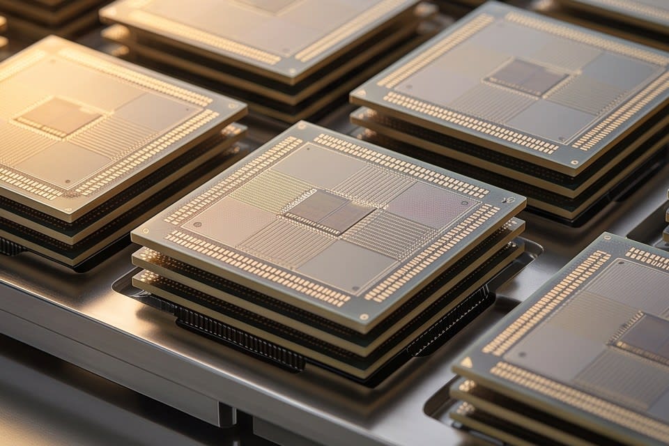
Just a few years ago, thickness control in semiconductor packages was measured by whether they were thin enough. But as AI semiconductors and high-performance memory have become mainstream, the more important question has shifted to how uniform they are. As structures that stack chips in multiple layers have become common, even a single thickness deviation has emerged as a variable that can undermine the reliability of the entire package. As stacked structures become more complex, precision machining and cleaning technologies will become even more decisive standards for process quality.
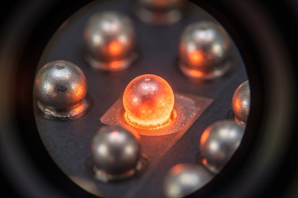
Why Thickness Uniformity Is a Key Quality Variable in Stacked Packaging
In 3D IC packaging structures where chips are stacked vertically, thickness uniformity is not simply a dimensional issue. The solder microbumps that connect the chips between each layer repeatedly contract and expand during thermal cycling, and if there is variation in chip thickness, the stress distribution concentrated on the bumps changes. According to research published on ScienceDirect, thermal cycling tests of 3D IC packaging showed that creep in solder microbumps, plastic deformation caused by high-temperature load, can increase by up to 50%, directly affecting thermomechanical reliability.
The greater the thickness deviation, the more stress becomes concentrated on specific bumps, and package warpage also worsens. As the number of stacked layers increases, the allowable tolerance range for each layer inevitably becomes narrower. When thickness nonuniformity in a single chip accumulates, the flatness of the entire package collapses, leading to bonding defects or electrical shorts in subsequent processes. In the end, thickness variation may not be visible, but it appears directly in the reliability metrics of the final product. As stacked packaging advances, securing thickness uniformity is becoming the starting point of process quality.
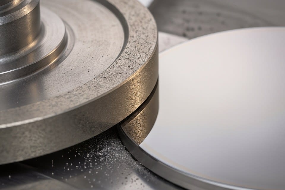
Limitations of Conventional Machining Methods and the Role of Precision Grinding Technology
Conventional grinding and chemical mechanical polishing have long been used as standards in semiconductor thinning processes, but their limitations are clear at the level of precision required by advanced packaging. According to an analysis by Eureka PatSnap, conventional grinding and chemical mechanical polishing processes often exceed thickness deviations of ±2μm, falling short of the latest package specifications that require submicron precision. As package types become more diverse, such as FCBGA, WLCSP, and QFN·DFN, and target thickness values vary, it is difficult for a single method to handle all specifications with the same level of precision.
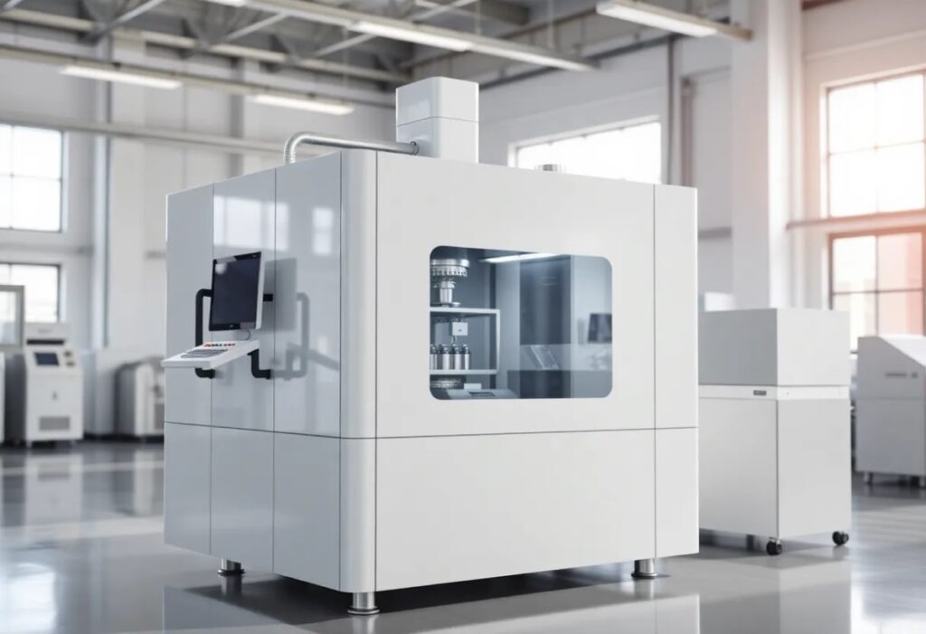
The moment deviation exceeds ±2μm, the package fails to meet the flatness criteria required in the next process, directly leading to yield loss. Micron-level grinding that combines a high-precision stage with a diamond wheel is one approach to closing this gap, and the same analysis shows that it can reduce material waste by 15 to 30% compared with conventional methods. Equipment such as a PKG Grinder, which supports both fully automatic and manual configurations, is designed to secure stable thickness precision in high-speed processes while maintaining production line flexibility. More important than which method is chosen is first defining the target package specification and allowable tolerance, then selecting the machining method that fits them.
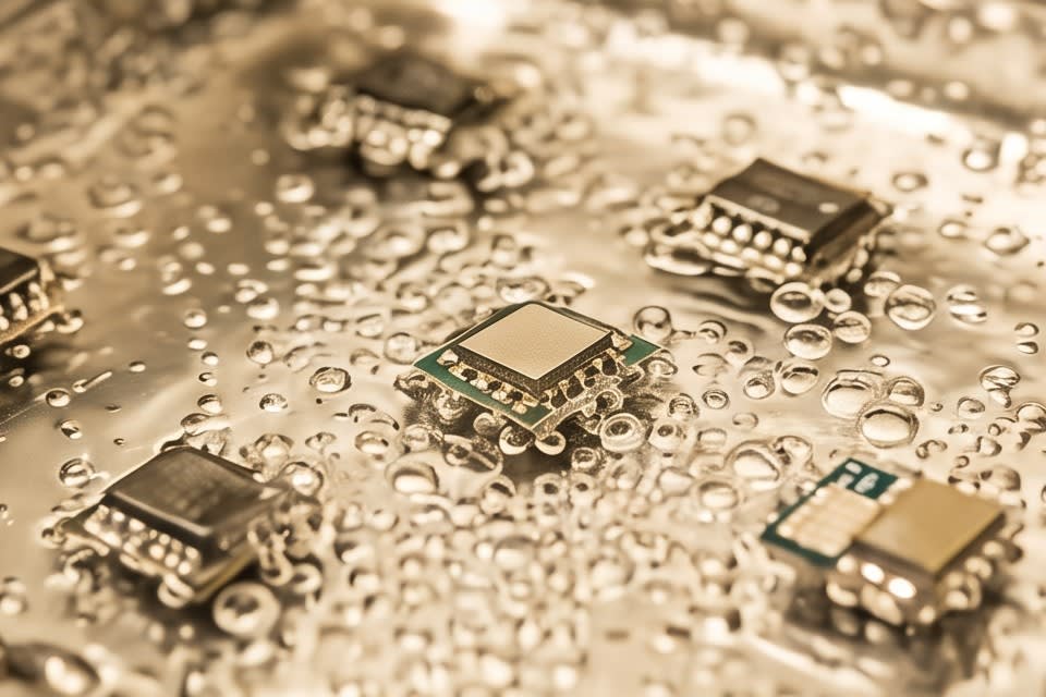
How the Cleaning Process Determines Final Quality
If precision machining reduces thickness variation, the cleaning process determines the surface condition before the result moves on to the next stage. For components that require ultra-precision optical and electrical characteristics, such as camera modules or autonomous driving sensors, even a single fine particle left after grinding can result in a defect judgment. In the field, cleaning is often regarded as the last step, but in practice it is the process that determines final quality.
According to research published in MDPI, cleaning solutions containing micro-nano bubbles improve the photoresist removal rate by 30%. A multistage cleaning method that applies Micro Bubble, Water Jet, and Air Knife step by step is structured to separate and discharge contaminant particles at each stage that are difficult to remove with a single method. For parts with complex shapes, such as VCM motors or semiconductor trays, the combination and sequence design of cleaning methods directly affect removal efficiency. When residual moisture is also removed through the Oven Dry process after cleaning, the possibility of secondary contamination in subsequent assembly or inspection processes is reduced.
Lower defect rates and stable yield ultimately come from how precisely the surface is controlled at this cleaning stage. The fact that invisible particles determine the quality of the entire process becomes clear the moment cleaning results are connected to shipping quality.
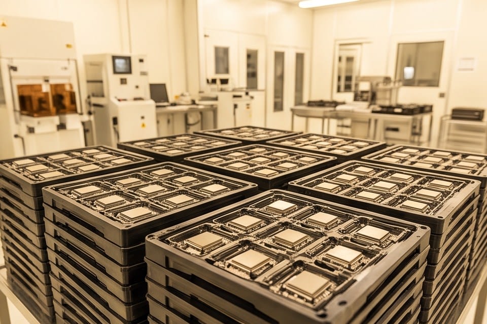
Reducing defects in semiconductor processes is not a matter of just one step. Package reliability is secured only when two processes work together: precision grinding that controls thickness variation at the micron level, and multistage cleaning that removes surface contaminant particles step by step. In a structure where the precision of each individual process determines the yield and reliability of the final product, which technologies are selected and how they are combined become practical benchmarks of manufacturing competitiveness.
Huvics is an advanced technology company that develops and manufactures automation equipment and
production systems across the semiconductor, LED, Mobile, and Cosmetic industries.
With top talent and continuous technological innovation, we help customers improve productivity and
secure quality competitiveness.
Huvics Contact
Tel: 031-374-8285
Email: cdpark@huvics.com