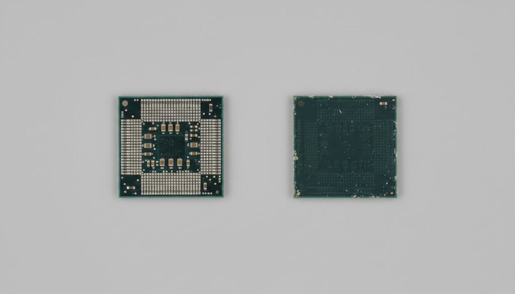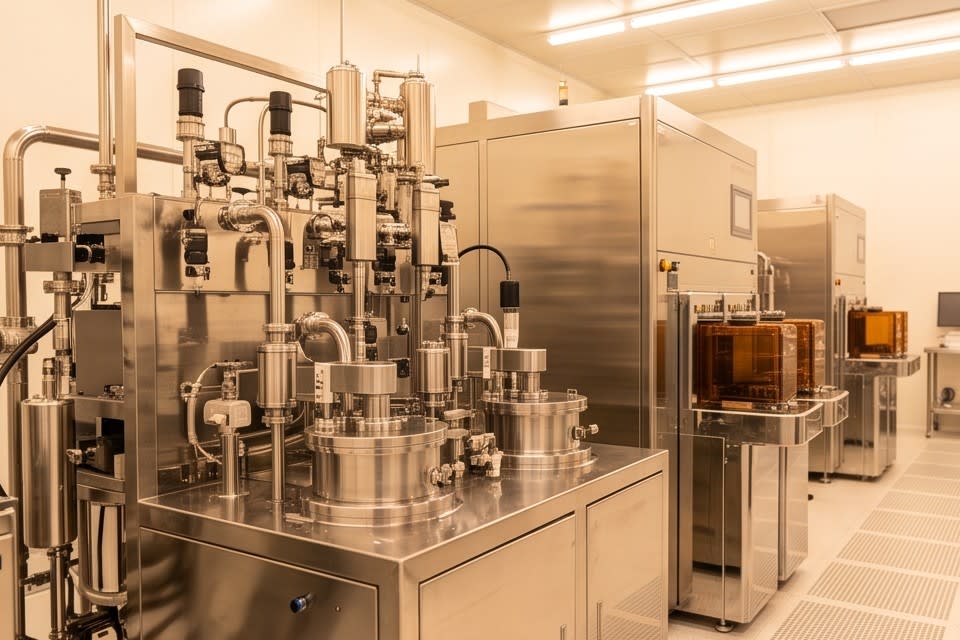
In semiconductor processes, cleaning was long considered a finishing stage. It was widely viewed as a supporting procedure that removes foreign matter before moving on to the next process. However, as chip integration has increased and package structures have become more complex, we have entered an era where a single cleaning method can determine overall yield. What type of bubbles are used, in what sequence drying takes place, and at what pressure cleaning is performed are now treated as key variables in process design.

Two Requirements of Cleaning Technology: Removal and Preservation
The core of cleaning technology lies in removing contaminant particles while fully preserving the product surface. These two requirements conflict with each other. Increasing cleaning power raises the risk of surface damage, while choosing a safer method can leave residual contamination behind.
The micro jet method instantaneously generates energy reaching thousands of atmospheres and thousands of degrees, and for fine pattern structures below 70 nanometers, this energy itself can become a source of damage. For this reason, in cleaning equipment design, energy control and dispersion methods become key criteria that define the level of technology.
The micro-nano bubble method distributes bubbles with a diameter of 0.1 micrometers or less in water to separate surface contamination, an approach designed to secure cleaning performance without physical impact. Multi-stage cleaning design combines different principles in this way to respond to the types of contamination generated at each process step.
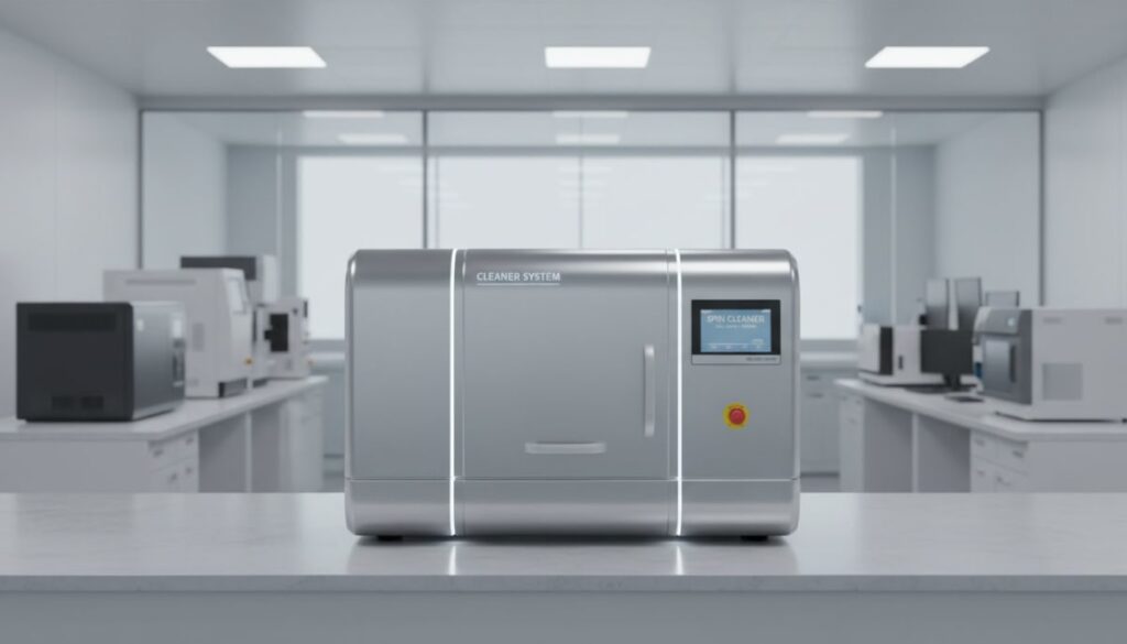
For products with complex surface structures and sensitive internal components, such as camera modules, sensors, and VCM motors, the limitations of a single cleaning method are clear. Combining Micro Bubble, Water Jet, and Air Knife step by step, while controlling residual moisture through Oven Dry functionality, is a configuration designed to meet these complex requirements. In processes where cleaning quality is directly linked to the final defect rate, which technology combination to choose is no longer a matter of equipment specifications, but a matter of process strategy.
Package Thickness Uniformity and Ultra-Precision Grinding Technology
Another variable that determines the quality of semiconductor processes as much as cleaning technology is the uniformity of package thickness. In structures where multiple chips are vertically stacked, such as AI semiconductors and high-performance memory, thickness variation in each layer affects both electrical characteristics and mechanical reliability. It is also known that in RF applications, substrate thickness and resistivity affect parasitic capacitance, thereby determining signal integrity.
The semiconductor industry roadmap requires wafer bonding processes to achieve thickness uniformity within ±5% across the entire wafer surface. If this standard is not met, stacking itself becomes meaningless.
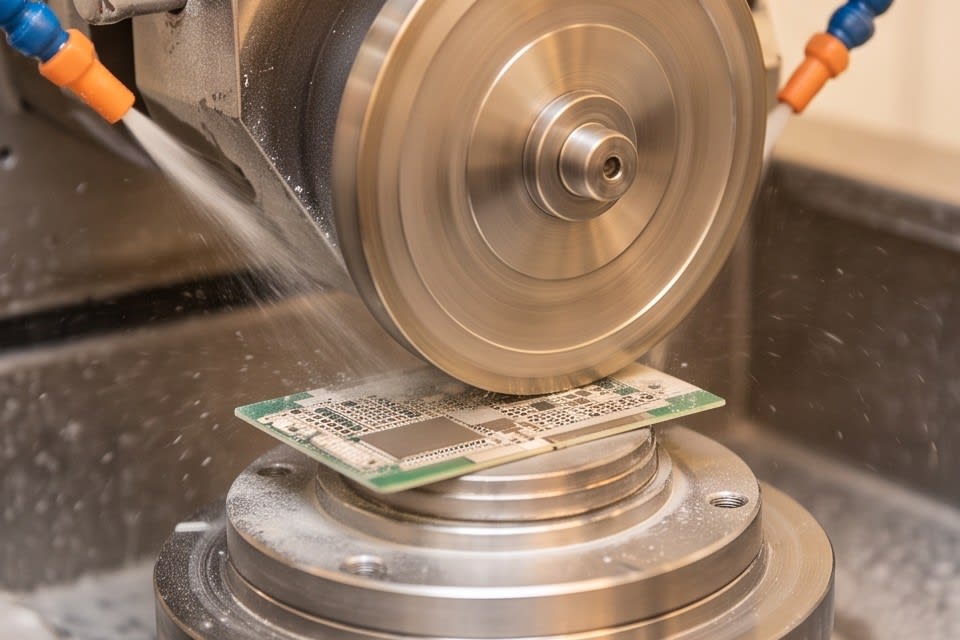
Huvics PKG Grinder performs micron-level grinding for various package types such as FCBGA, WLCSP, and QFN/DFN by using a high-precision stage and diamond wheel. It is available in Full Auto and Manual Type configurations to secure production line flexibility while being designed to maintain consistent thickness uniformity in high-speed processes. Regardless of which package structure is selected, how tightly thickness variation is managed is the key factor that separates product grade and yield.

The Impact of Automation Transition on Yield and Availability
As the precision of process technology increases, the importance of how equipment is operated to implement it consistently also grows. Processes manually performed by skilled operators rely on individual experience and judgment, which creates structural limitations in repeatability and reproducibility. Even with the same equipment, results vary depending on the operating method, and those differences lead to yield variation in mass-production environments.
Cases have been reported in which efficiency increased by approximately 17.6% when a systematic yield improvement framework was introduced compared with manual empirical methods. Automation transition is not simply a matter of increasing speed, but of securing process consistency and predictability. According to a McKinsey report, improving equipment reliability can increase tool availability in fabs by more than 15%. Higher availability means fewer unplanned equipment stops and maintenance gaps, which connects directly to the stability of the overall production plan.
A configuration that combines Full Auto and Manual options is a strategy for flexibly responding to these needs, and many cases have accumulated in manufacturing sites where the level of process automation has been increased step by step.
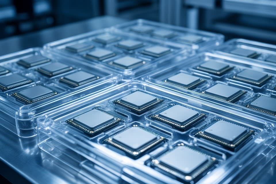
In semiconductor processes, cleaning and grinding may appear to be separate technical domains, but they ultimately converge on the same question. How should the surface be handled so that the next process can proceed reliably. Bubble size, pressure control, thickness uniformity, equipment availability, all these variables make up the details of the process, and the sum of those details determines the reliability of the final product. Yield is not reserved at the design stage, but is protected or lost at every step of the process.
Huvics is an advanced technology company that develops and manufactures automation equipment and
production systems across the semiconductor, LED, Mobile, and Cosmetic industries.
With top talent and continuous technological innovation, we support customers in improving productivity and
securing quality competitiveness.
Huvics Contact Information
Phone: 031-374-8285
Email: cdpark@huvics.com