-
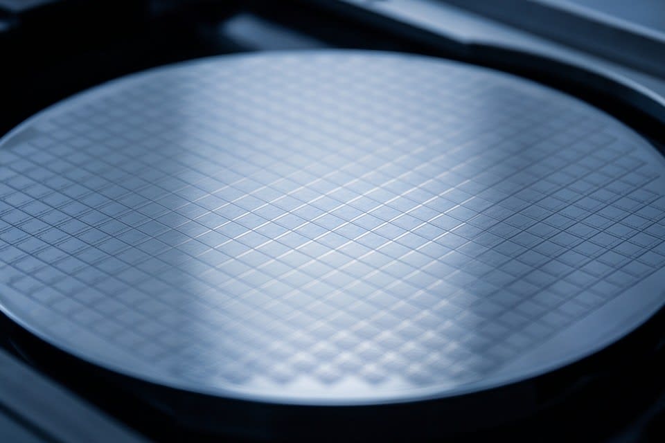
A Field Case That Made the Difference Between 95% and 75% Yield, How Are You Designing Your Cleaning Process?
In semiconductor manufacturing sites, some view the cleaning process as the ‘finishing stage’. However, the fact that a single contaminant particle can change the fate of an entire wafer shows that cleaning is not the end of the process, but a… “View more”
-
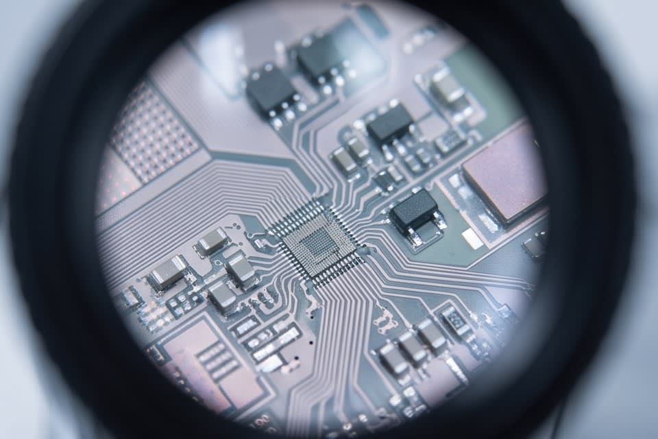
In semiconductor processes, it is not uncommon for a single defect to lead to the disposal of an entire finished product. According to an analysis by Elementary ML, automated optical inspection systems can… <View more>
-
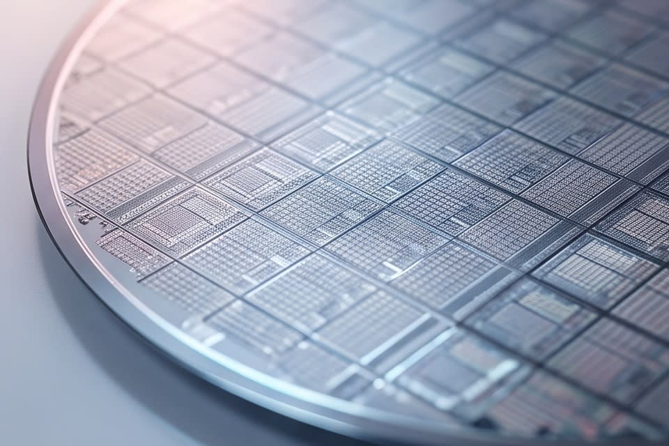
According to a study published by ScienceDirect in 2026, the accuracy of machine learning based semiconductor defect detection and classification reached 98 to 99% in some inspection tasks, with performance improvements reported to be 4.6 to 8.6 times higher than conventional methods. These figures show that semiconductor manufacturing… <View more>